TLV5608
TLV5610
TLV5629
www.ti.com.................................................................................................................................................... SLAS268G – MAY 2000 – REVISED NOVEMBER 2008
8-CHANNEL, 12-/10-/8-BIT, 2.7-V TO 5.5-V LOW POWER
DIGITAL-TO-ANALOG CONVERTER WITH POWER DOWN
FEATURES
APPLICATIONS
• Eight Voltage Output DACs in One Package
– TLV5610 . . . 12-Bit
– TLV5608 . . . 10-Bit
– TLV5629 . . . 8-Bit
• Programmable Settling Time vs Power
Consumption
– 1 µs In Fast Mode
– 3 µs In Slow Mode
• Compatible With TMS320 and SPI™ Serial
Ports
• Monotonic Over Temperature
• Low Power Consumption:
– 18 mW In Slow Mode at 3-V
– 48 mW In Fast Mode at 3-V
• Reference Input Buffers
• Power-Down Mode
• Buffered, High Impedance Reference Inputs
• Data Output for Daisy-Chaining
•
•
•
•
•
1
2
Digital Servo Control Loops
Digital Offset and Gain Adjustment
Industrial Process Control
Machine and Motion Control Devices
Mass Storage Devices
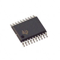
DW OR PW PACKAGE
(TOP VIEW)
1
2
3
4
5
6
7
8
9
10
DGND
DIN
SCLK
FS
PRE
OUTE
OUTF
OUTG
OUTH
AGND
20
19
18
17
16
15
14
13
12
11
DVDD
DOUT
LDAC
MODE
REF
OUTD
OUTC
OUTB
OUTA
AVDD
DESCRIPTION
The TLV5610, TLV5608, and TLV5629 are pin-compatible, eight-channel, 12-/10-/8-bit voltage output DACs
each with a flexible serial interface. The serial interface allows glueless interface to TMS320 and SPI, QSPI, and
Microwire serial ports. It is programmed with a 16-bit serial string containing 4 control and 12 data bits.
Additional features are a power-down mode, an LDAC input for simultaneous update of all eight DAC outputs,
and a data output which can be used to cascade multiple devices.
The resistor string output voltage is buffered by a rail-to-rail output amplifier with a programmable settling time to
allow the designer to optimize speed vs power dissipation. The buffered, high-impedance reference input can be
connected to the supply voltage.
Implemented with a CMOS process, the DACs are designed for single-supply operation from 2.7 V to 5.5 V, and
can operate on two separate analog and digital power supplies. The devices are available in 20-pin SOIC and
TSSOP packages.
AVAILABLE OPTIONS
TA
PACKAGE
SMALL OUTLINE (DW)
TSSOP (PW)
RESOLUTION
TLV5610IDW
TLV5610IPW
12
TLV5608IDW
TLV5608IPW
10
TLV5629IDW
TLV5629IPW
8
-40°C to 85°C
1
2
Please be aware that an important notice concerning availability, standard warranty, and use in critical applications of Texas
Instruments semiconductor products and disclaimers thereto appears at the end of this data sheet.
SPI is a trademark of Motorola, Inc.
PRODUCTION DATA information is current as of publication date.
Products conform to specifications per the terms of the Texas
Instruments standard warranty. Production processing does not
necessarily include testing of all parameters.
Copyright © 2000–2008, Texas Instruments Incorporated
�TLV5608
TLV5610
TLV5629
SLAS268G – MAY 2000 – REVISED NOVEMBER 2008.................................................................................................................................................... www.ti.com
These devices have limited built-in ESD protection. The leads should be shorted together or the device placed in conductive foam
during storage or handling to prevent electrostatic damage to the MOS gates.
FUNCTIONAL BLOCK DIAGRAM
REF
12/10/8
12/10/8
12/10/8
X2
DAC A
Holding
Latch
OUTA
DAC A
Latch
SCLK
DIN
DOUT
12
Serial
Interface
FS
8
DAC B, C, D, E, F, G and H
Same as DAC A
MODE
PRE
OUT
B, C, D,
E, F, G
and H
LDAC
Terminal Functions
TERMINAL
I/O
DESCRIPTION
NAME
NO.
AGND
10
I
Analog ground
AVDD
11
I
Analog power supply
DGND
1
I
Digital ground
DIN
2
I
Digital serial data input
DOUT
19
O
Digital serial data output
DVDD
20
I
Digital power supply
FS
4
I
Frame sync input
LDAC
18
I
Load DAC. The DAC outputs are only updated, if this signal is low. It is an
asynchronous input.
MODE
17
I
DSP/µC mode pin. High = µC mode, NC = DSP mode.
PRE
5
I
Preset input
REF
16
I
Voltage reference input
SCLK
3
I
Serial clock input
6-9, 12-15
O
DAC outputs A, B, C, D, E, F, G and H
OUTA-OUTH
2
Submit Documentation Feedback
Copyright © 2000–2008, Texas Instruments Incorporated
Product Folder Link(s): TLV5608 TLV5610 TLV5629
�TLV5608
TLV5610
TLV5629
www.ti.com.................................................................................................................................................... SLAS268G – MAY 2000 – REVISED NOVEMBER 2008
ABSOLUTE MAXIMUM RATINGS
over operating free-air temperature range (unless otherwise noted) (1)
UNIT
Supply voltage (AVDD, DVDD to GND)
7V
Reference input voltage
- 0.3 V to AVDD + 0.3 V
Digital input voltage range
- 0.3 V to DVDD + 0.3 V
Operating free-air temperature range, TA
-40°C to 85°C
Storage temperature range, Tstg
-65°C to 150°C
Lead temperature 1,6 mm (1/16 inch) from case for 10 seconds
(1)
260°C
Stresses beyond those listed under absolute maximum ratings may cause permanent damage to the device. These are stress ratings
only, and functional operation of the device at these or any other conditions beyond those indicated under recommended operating
conditions is not implied. Exposure to absolute-maximum-rated conditions for extended periods may affect device reliability.
RECOMMENDED OPERATING CONDITIONS
Supply voltage, AVDD, DVDD
High-level digital input voltage, VIH
Low-level digital input voltage, VIL
Reference voltage, Vref
MIN
NOM
MAX
5-V operation
4.5
5
5.5
UNIT
V
3-V operation
2.7
3
3.3
V
DVDD = 2.7 V
2
DVDD = 5.5 V
2.4
V
DVDD = 2.7 V
0.6
DVDD = 5.5 V
1
V
AVDD = 5 V
GND
4.096
AVDD
V
AVDD = 3 V
GND
2.048
AVDD
V
Load resistance, RL
2
kΩ
Load capacitance, CL
100
pF
Clock frequency, fCLK
30
MHz
85
°C
Operating free-air temperature, TA
-40
ELECTRICAL CHARACTERISTICS
over recommended operating free-air temperature range, supply voltages, and reference voltages (unless otherwise noted)
PARAMETER
TEST CONDITIONS
MIN
TYP
MAX
16
21
6
8
UNIT
POWER SUPPLY
IDD
Power supply current
Fast
Slow
No load, Vref = 4.096 V, See
All inputs = DVDD or GND
(1)
Power down supply current
POR
Power on threshold
PSRR
Power supply rejection ratio
(1)
(2)
0.1
Full scale, See
(2)
mA
µA
2
V
-60
dB
IDD is measured while continuously writing code 2048 to the DAC. For VIH < DVDD - 0.7 V and VIL > 0.7 V, supply current increases.
Power supply rejection ratio at full scale is measured by varying AVDD and is given by:
PSRR = 20 log [(EG(AVDDmax) - EG(AVDDmin))/VDDmax]
Copyright © 2000–2008, Texas Instruments Incorporated
Product Folder Link(s): TLV5608 TLV5610 TLV5629
Submit Documentation Feedback
3
�TLV5608
TLV5610
TLV5629
SLAS268G – MAY 2000 – REVISED NOVEMBER 2008.................................................................................................................................................... www.ti.com
ELECTRICAL CHARACTERISTICS (continued)
over recommended operating free-air temperature range, supply voltages, and reference voltages (unless otherwise noted)
PARAMETER
TEST CONDITIONS
MIN
TYP
MAX
UNIT
STATIC DAC SPECIFICATIONS
Resolution
TLV5610
12
TLV5608
10
TLV5629
8
TLV5610
Integral nonlinearity (INL)
Differential nonlinearity (DNL)
TLV5608
Code 40 to 4095
±2
±6
Code 20 to 1023
±0.5
±2
TLV5629
Code 6 to 255
±0.3
±1
TLV5610
Code 40 to 4095
±0.5
±1
Code 20 to 1023
±0.1
±1
Code 6 to 255
±0.1
±1
TLV5608
Vref = 2 V, 4V
Bits
Vref = 2 V, 4V
TLV5629
EZS
Zero-scale error (offset error at zero scale)
EZS TC
Zero-scale-error temperature coefficient
EG
Gain error
EG TC
Gain error temperature coefficient
±30
LSB
LSB
mV
µV/°C
30
±0.6
10
% of FS
voltage
ppm/°C
OUTPUT SPECIFICATIONS
VO
Voltage output range
RL = 10 kΩ
Output load regulation accuracy
RL = 2 kΩ vs 10 kΩ
AVDD 0.4
0
V
±0.3
% of FS
voltage
AVDD
V
REFERENCE INPUT
VI
Reference input voltage
RI
Reference input resistance
CI
Reference input capacitance
0
100
kΩ
5
pF
Fast
Vref = 0.4 Vpp + 2.048 Vdc,
Input code = 0x800
2.2
Slow
Vref = 2 Vpp at 1 kHz + 2.048 Vdc,
See (3)
1.9
Reference input bandwidth
MHz
Reference feedthrough
-84
dB
DIGITAL INPUT
IIH
High-level digital input current
VI = VDD
IIL
Low-level digital input current
VI = 0 V
CI
Input capacitance
1
µA
µA
-1
8
pF
DIGITAL OUTPUT
VOH
High-level digital output voltage
RL = 10 kΩ
VOL
Low-level digital output voltage
RL = 10 kΩ
Output voltage rise time
RL = 10 kΩ, CL = 20 pF, Includes
propagation delay
(3)
4
2.6
V
7
0.4
V
20
ns
Reference feedthrough is measured at the DAC output with an input code = 0x000.
Submit Documentation Feedback
Copyright © 2000–2008, Texas Instruments Incorporated
Product Folder Link(s): TLV5608 TLV5610 TLV5629
�TLV5608
TLV5610
TLV5629
www.ti.com.................................................................................................................................................... SLAS268G – MAY 2000 – REVISED NOVEMBER 2008
ELECTRICAL CHARACTERISTICS (continued)
over recommended operating free-air temperature range, supply voltages, and reference voltages (unless otherwise noted)
PARAMETER
TEST CONDITIONS
MIN
TYP
MAX
1
3
3
7
0.5
1
1
2
UNIT
ANALOG OUTPUT DYNAMIC PERFORMANCE
ts(FS)
Output settling time (full scale)
ts(CC)
Output settling time, code to
code
SR
Slew rate
(4)
(5)
(6)
(7)
Fast
Slow
Fast
Slow
Fast
Slow
RL = 10 kΩ, CL = 100 pF, See
(4)
RL = 10 kΩ, CL = 100 pF, See
(5)
RL = 10 kΩ, CL = 100 pF, See
(6)
4
10
1
3
(7)
Glitch energy
See
Channel crosstalk
10 kHz sine, 4 VPP
µs
µs
V/µs
4
nV-s
-90
dB
Settling time is the time for the output signal to remain within +0.5 LSB of the final measured value for a digital input code change of
0x80 to 0xFFF and 0xFFF to 0x080, respectively. Assured by design; not tested.
Settling time is the time for the output signal to remain within +0.5 LSB of the final measured value for a digital input code change of one
count. The max time applies to code changes near zero scale or full scale. Assured by design; not tested.
Slew rate determines the time it takes for a change of the DAC output from 10% to 90% full scale voltage.
Code transition: TLV5610 - 0x7FF to 0x800, TLV5608 - 0x7FC to 0x800, TLV5629 - 0x7F0 to 0x800
TIMING REQUIREMENTS
DIGITAL INPUTS
MIN
tsu(FS-CK)
Setup time, FS low before next negative SCLK edge
NOM
MAX
UNIT
8
ns
tsu(C16-FS)
Setup time, 16th negative edge after FS low on which bit D0 is sampled before
rising edge of FS. µC mode only
10
ns
tsu(FS-C17)
µC mode, setup time, FS high before 17 negative edge of SCLK.
10
ns
tsu(CK-FS)
DSP mode, setup time, SLCK low before FS low.
5
ns
twL(LDAC)
LDAC duration low
10
ns
twH
SCLK pulse duration high
16
ns
twL
SCLK pulse duration low
16
ns
tsu(D)
Setup time, data ready before SCLK falling edge
8
ns
th(D)
Hold time, data held valid after SCLK falling edge
5
ns
twH(FS)
FS duration high
10
ns
twL(FS)
FS duration low
10
ns
ts
Settling time
th
See AC
specs
Copyright © 2000–2008, Texas Instruments Incorporated
Product Folder Link(s): TLV5608 TLV5610 TLV5629
Submit Documentation Feedback
5
�TLV5608
TLV5610
TLV5629
SLAS268G – MAY 2000 – REVISED NOVEMBER 2008.................................................................................................................................................... www.ti.com
PARAMETER MEASUREMENT INFORMATION
t wH
t wL
SCLK
X
1
2
3
4
16
17
X
t h(D)
t su(D)
DIN
X
D15
DOUT
X
D15
D14
†
D14
D13
†
D13
D12
†
D12
D1
†
D1
D0
†
D0
X
†
X
t su(FS - C17)
t su(FS - CK)
t wH(FS)
tsu(C16 - FS)
FS
(mC mode)
t su(CK - FS)
t wL(FS)
FS
(DSP Mode)
†
X
Previous input data
Figure 1. Serial Interface Timing
twL(LDAC)
LDAC
±0.5 LSB
ts
OUTx
Figure 2. Output Timing
6
Submit Documentation Feedback
Copyright © 2000–2008, Texas Instruments Incorporated
Product Folder Link(s): TLV5608 TLV5610 TLV5629
�TLV5608
TLV5610
TLV5629
www.ti.com.................................................................................................................................................... SLAS268G – MAY 2000 – REVISED NOVEMBER 2008
TYPICAL CHARACTERISTICS
OUTPUT LOAD REGULATION
OUTPUT LOAD REGULATION
1
1
VDD = 3 V,
Vref = 2 V,
Zero Scale
0.9
0.8
0.8
Fast
VO − Output Voltage − V
VO − Output Voltage − V
VDD = 5 V,
Vref = 4 V,
Zero Scale
0.9
0.7
0.6
0.5
0.4
0.3
Fast
0.7
0.6
0.5
0.4
0.3
0.2
0.2
0.1
0.1
Slow
Slow
0
0
0.5
0
1.5
1
Sinking Current − mA
0.5
0
2
Figure 3.
OUTPUT LOAD REGULATION
OUTPUT LOAD REGULATION
4.12
VDD = 3 V,
Vref = 2 V,
Full Scale
2.055
4.11
Slow
VO − Output Voltage − V
VO − Output Voltage − V
2
Figure 4.
2.06
2.05
1.5
1
Sinking Current − mA
Fast
2.045
2.04
2.035
VDD = 5 V,
Vref = 4 V,
Full Scale
Fast
4.1
Slow
4.09
4.08
4.07
4.06
2.03
2.025
−0.05 −0.5
4.05
4.04
−1
−1.5
−2
−2.5
−3
−3.5
−4
0
−0.5
−1
Sourcing Current − mA
Figure 5.
−1.5
−2
−2.5
−3
−3.5
−4
Sourcing Current − mA
Figure 6.
Copyright © 2000–2008, Texas Instruments Incorporated
Product Folder Link(s): TLV5608 TLV5610 TLV5629
Submit Documentation Feedback
7
�TLV5608
TLV5610
TLV5629
SLAS268G – MAY 2000 – REVISED NOVEMBER 2008.................................................................................................................................................... www.ti.com
TYPICAL CHARACTERISTICS (continued)
INL − Integral Nonlinearity − LSB
TLV5610
INTEGRAL NONLINEARITY
vs
CODE
4
3
2
1
0
−1
−2
−3
−4
0
1024
2048
3072
4096
3072
4096
Code
Figure 7.
DNL − Differential Nonlinearity − LSB
TLV5610
DIFFERENTIAL NONLINEARITY
vs
CODE
1.0
0.8
0.6
0.4
0.2
−0.0
−0.2
−0.4
−0.6
−0.8
−1.0
0
1024
2048
Code
Figure 8.
8
Submit Documentation Feedback
Copyright © 2000–2008, Texas Instruments Incorporated
Product Folder Link(s): TLV5608 TLV5610 TLV5629
�TLV5608
TLV5610
TLV5629
www.ti.com.................................................................................................................................................... SLAS268G – MAY 2000 – REVISED NOVEMBER 2008
TYPICAL CHARACTERISTICS (continued)
INL − Integral Nonlinearity − LSB
TLV5608
INTEGRAL NONLINEARITY
vs
CODE
2.0
1.5
1.0
0.5
0.0
−0.5
−1.0
−1.5
−2.0
0
256
512
768
1024
768
1024
Code
Figure 9.
DNL − Differential Nonlinearity − LSB
TLV5608
DIFFERENTIAL NONLINEARITY
vs
CODE
1.0
0.8
0.6
0.4
0.2
−0.0
−0.2
−0.4
−0.6
−0.8
−1.0
0
256
512
Code
Figure 10.
Copyright © 2000–2008, Texas Instruments Incorporated
Product Folder Link(s): TLV5608 TLV5610 TLV5629
Submit Documentation Feedback
9
�TLV5608
TLV5610
TLV5629
SLAS268G – MAY 2000 – REVISED NOVEMBER 2008.................................................................................................................................................... www.ti.com
TYPICAL CHARACTERISTICS (continued)
INL − Integral Nonlinearity − LSB
TLV5629
INTEGRAL NONLINEARITY
vs
CODE
0.5
0.4
0.3
0.2
0.1
0
−0.1
−0.2
−0.3
−0.4
−0.5
0
50
100
150
200
250
200
250
Code
Figure 11.
DNL − Differential Nonlinearity − LSB
TLV5629
DIFFERENTIAL NONLINEARITY
vs
CODE
0.5
0.4
0.3
0.2
0.1
0
−0.1
−0.2
−0.3
−0.4
−0.5
0
50
100
150
Code
Figure 12.
10
Submit Documentation Feedback
Copyright © 2000–2008, Texas Instruments Incorporated
Product Folder Link(s): TLV5608 TLV5610 TLV5629
�TLV5608
TLV5610
TLV5629
www.ti.com.................................................................................................................................................... SLAS268G – MAY 2000 – REVISED NOVEMBER 2008
APPLICATION INFORMATION
GENERAL FUNCTION
The TLV5610, TLV5608, and TLV5629 are 8-channel, 12-bit, single-supply DACs, based on a resistor string
architecture. They consist of a serial interface, a speed and power-down control logic, a reference input buffer, a
resistor string, and a rail-to-rail output buffer.
The output voltage (full scale determined by external reference) for each channel is given by:
REF CODE [V]
0x1000
(1)
where REF is the reference voltage and CODE is the digital input value. The input range is 0x000 to 0xFFF for
the TLV5610, 0x000 to 0xFFC for the TLV5608, and 0x000 to 0xFF0 for the TLV5629.
POWER ON RESET (POR)
The built-in power-on-reset circuit controls the output voltage after power up. On power up, all latches including
the preset register are set to zero, but the DAC outputs are only set to zero if the LDAC is low. The DAC outputs
may have a small offset error produced by the output buffer. The registers remains at zero until a valid write
sequence is made to the DAC, changing the DAC register data. This is useful in applications where it is
important to know the state of the outputs of the DAC after power up. All digital inputs must be logic low until the
digital and analog supplies are applied. Any logic high voltages applied to the logic input pins when power is not
applied to AVDD and DVDD, may power the device logic circuit through the overvoltage protection diode causing
an undesired operation. When separate analog (AVDD) and digital (DVDD) supplies are used, AVDD must come up
first before DVDD, to ensure that the power-on-reset circuit operates correctly.
SERIAL INTERFACE
A falling edge of FS starts shifting the data on DIN starting with the MSB to the internal register on the falling
edges of SCLK. After 16 bits have been transferred, the content of the shift register is moved to one of the DAC
holding registers, depending on the address bits within the data word. A logic 0 on the LDAC pin is required to
transfer the content of the DAC holding register to the DAC latch and to update the DAC outputs. LDAC is an
asynchronous input. It can be held low if a simultaneous update of all eight channels is not needed.
For daisy-chaining, DOUT provides the data sampled on DIN with a delay of 16 clock cycles.
DSP Mode:
SCLK
FS
DIN
X
D15
D14
D1
D0
E15
E14
X
D15
D14
D1
D0
X
E15
E1
E0
X
E1
E0
X
X
F15
F15
X
F15
F15
µC Mode:
SCLK
FS
DIN
E14
X
Figure 13. Data Sampled on DIN
Copyright © 2000–2008, Texas Instruments Incorporated
Product Folder Link(s): TLV5608 TLV5610 TLV5629
Submit Documentation Feedback
11
�TLV5608
TLV5610
TLV5629
SLAS268G – MAY 2000 – REVISED NOVEMBER 2008.................................................................................................................................................... www.ti.com
Difference between DSP mode (MODE = N.C. or 0) and µC (MODE = 1) mode:
• In µC mode, FS needs to be held low until all 16 data bits have been transferred. If FS is driven high before
the 16th falling clock edge, the data transfer is cancelled. The DAC is updated after a rising edge on FS.
• In DSP mode, FS needs to stay low for 20 ns and can go high before the 16th falling clock edge.
• In DSP mode there needs to be one falling SCLK edge before FS goes low to start the write (DIN) cycle. This
extra falling SCLK edge has to happen at least 5 ns before FS goes low, tsu(CK-FS) ≥ 5 ns.
• In µC mode, the extra falling SCLK edge is not necessary. However, if it does happen, the extra negative
SCLK edge is not allowed to occur within 10 ns after FS goes HIGH to finish the WRITE cycle (tsu(FS-C17)).
SERIAL CLOCK FREQUENCY AND UPDATE RATE
The maximum serial clock frequency is given by:
1
f
+
+ 30 MHz
sclkmax
t
)t
whmin
wlmin
(2)
The maximum update rate is:
1
f
+
+ 1.95 MHz
updatemax
Ǔ
16 ǒt
)t
whmin
wlmin
(3)
Note, that the maximum update rate is just a theoretical value for the serial interface, as the settling time of the
DAC has to be considered also.
DATA FORMAT
The 16-bit data word consists of two parts:
• Address bits (D150D12)
• Data bits (D110D0)
D15
D14
D13
D12
A3
A2
A1
A0
D11
D10
D9
D8
D7
D6
D5
D4
D3
D2
D1
D0
DATA
Register Map
12
A3
A2
A1
A0
FUNCTION
0
0
0
0
DAC A
0
0
0
1
DAC B
0
0
1
0
DAC C
0
0
1
1
DAC D
0
1
0
0
DAC E
0
1
0
1
DAC F
0
1
1
0
DAC G
0
1
1
1
DAC H
1
0
0
0
CTRL0
1
0
0
1
CTRL1
1
0
1
0
Preset
1
0
1
1
Reserved
1
1
0
0
DAC A and B
1
1
0
1
DAC C and D
1
1
1
0
DAC E and F
1
1
1
1
DAC G and H
Submit Documentation Feedback
Copyright © 2000–2008, Texas Instruments Incorporated
Product Folder Link(s): TLV5608 TLV5610 TLV5629
�TLV5608
TLV5610
TLV5629
www.ti.com.................................................................................................................................................... SLAS268G – MAY 2000 – REVISED NOVEMBER 2008
DAC A-H AND TWO-CHANNEL REGISTERS
Writing to DAC A-H sets the output voltage of channel A-H. It is possible to automatically generate the
complement of one channel by writing to one of the four two-channel registers (DAC A and B etc.).
The TLV5610 decodes all 12 data bits. The TLV5608 decodes D11 to D2 (D1 and D0 are ignored). The TLV5629
decodes D11 to D4 (D3 to D0 are ignored).
PRESET
The outputs of the DAC channels can be driven simultaneously to a predefined value stored in the preset register
by driving the PRE input pin low and asserting the LDAC input pin. The preset register is cleared (set to zero) by
the POR circuit after power up. Therefore, it must be written with a predefined value before asserting the PRE
pin low, unless zero is the desired preset value. The PRE input is asynchronous to the clock.
CTRL0
D11
D10
D9
D8
D7
D6
D5
D4
D3
D2
D1
D0
X
X
X
X
X
X
X
PD
DO
X
X
IM
PD
: Full device power down
0 = normal
1 = power down
DO
: Digital output enable
0 = disable
1 = enable
IM
: Input mode
0 = straight binary
1 = twos complement
X
: Reserved
If DOUT is enabled, the data input on DIN is output on DOUT with a 16-cycle delay. That makes it possible to
daisy-chain multiple DACs on one serial bus.
CTRL1
D11
D10
D9
D8
D7
D6
D5
D4
D3
D2
D1
D0
X
X
X
X
PGH
PEF
PCD
PAB
SGH
SEF
SCD
SAB
PXY
: Power down DACXY
0 = normal
1 = power down
SXY
: Speed DACXY
0 = slow
1 = fast
XY
: DAC pair AB, CD, EF, or GH
In power-down mode, the amplifiers of the selected DAC pair within the device are disabled and the total power
consumption of the device is significantly reduced. Power-down mode of a specific DAC pair can be selected by
setting the PXY bit within the data word to 1.
There are two settling time modes: fast and slow. Fast mode of a DAC pair is selected by setting SXY to 1 and
slow mode is selected by setting SXY to 0.
REFERENCE
The DAC reference can be sourced externally using precision reference circuits. Since the reference input is
buffered, it can be connected to the supply voltage.
BUFFERED AMPLIFIER
The DAC outputs are buffered by an amplifier with a gain of two, which are configurable as Class A (fast mode)
or Class AB (slow or low-power mode). The output buffers have near rail-to-rail output with short-circuit
protection, and can reliably drive a 2-kΩ load with a 100-pF load capacitance.
Copyright © 2000–2008, Texas Instruments Incorporated
Product Folder Link(s): TLV5608 TLV5610 TLV5629
Submit Documentation Feedback
13
�PACKAGE OPTION ADDENDUM
www.ti.com
14-Oct-2022
PACKAGING INFORMATION
Orderable Device
Status
(1)
Package Type Package Pins Package
Drawing
Qty
Eco Plan
(2)
Lead finish/
Ball material
MSL Peak Temp
Op Temp (°C)
Device Marking
(3)
Samples
(4/5)
(6)
TLV5608IDW
ACTIVE
SOIC
DW
20
25
RoHS & Green
NIPDAU
Level-1-260C-UNLIM
-40 to 85
TLV5608I
Samples
TLV5608IDWR
ACTIVE
SOIC
DW
20
2000
RoHS & Green
NIPDAU
Level-1-260C-UNLIM
-40 to 85
TLV5608I
Samples
TLV5608IPW
ACTIVE
TSSOP
PW
20
70
RoHS & Green
NIPDAU
Level-1-260C-UNLIM
-40 to 85
TY5608
Samples
TLV5608IPWR
ACTIVE
TSSOP
PW
20
2000
RoHS & Green
NIPDAU
Level-1-260C-UNLIM
-40 to 85
TY5608
Samples
TLV5608IPWRG4
ACTIVE
TSSOP
PW
20
2000
RoHS & Green
NIPDAU
Level-1-260C-UNLIM
-40 to 85
TY5608
Samples
TLV5610IDW
ACTIVE
SOIC
DW
20
25
RoHS & Green
NIPDAU
Level-1-260C-UNLIM
-40 to 85
TLV5610I
Samples
TLV5610IDWR
ACTIVE
SOIC
DW
20
2000
RoHS & Green
NIPDAU
Level-1-260C-UNLIM
-40 to 85
TLV5610I
Samples
TLV5610IPW
ACTIVE
TSSOP
PW
20
70
RoHS & Green
NIPDAU
Level-1-260C-UNLIM
-40 to 85
TY5610
Samples
TLV5610IPWR
ACTIVE
TSSOP
PW
20
2000
RoHS & Green
NIPDAU
Level-1-260C-UNLIM
-40 to 85
TY5610
Samples
TLV5629IDW
ACTIVE
SOIC
DW
20
25
RoHS & Green
NIPDAU
Level-1-260C-UNLIM
-40 to 85
TLV5629I
Samples
TLV5629IDWG4
ACTIVE
SOIC
DW
20
25
RoHS & Green
NIPDAU
Level-1-260C-UNLIM
-40 to 85
TLV5629I
Samples
TLV5629IDWR
ACTIVE
SOIC
DW
20
2000
RoHS & Green
NIPDAU
Level-1-260C-UNLIM
-40 to 85
TLV5629I
Samples
TLV5629IPW
ACTIVE
TSSOP
PW
20
70
RoHS & Green
NIPDAU
Level-1-260C-UNLIM
-40 to 85
TY5629
Samples
TLV5629IPWG4
ACTIVE
TSSOP
PW
20
70
RoHS & Green
NIPDAU
Level-1-260C-UNLIM
-40 to 85
TY5629
Samples
TLV5629IPWR
ACTIVE
TSSOP
PW
20
2000
RoHS & Green
NIPDAU
Level-1-260C-UNLIM
-40 to 85
TY5629
Samples
(1)
The marketing status values are defined as follows:
ACTIVE: Product device recommended for new designs.
LIFEBUY: TI has announced that the device will be discontinued, and a lifetime-buy period is in effect.
NRND: Not recommended for new designs. Device is in production to support existing customers, but TI does not recommend using this part in a new design.
PREVIEW: Device has been announced but is not in production. Samples may or may not be available.
OBSOLETE: TI has discontinued the production of the device.
Addendum-Page 1
�PACKAGE OPTION ADDENDUM
www.ti.com
14-Oct-2022
(2)
RoHS: TI defines "RoHS" to mean semiconductor products that are compliant with the current EU RoHS requirements for all 10 RoHS substances, including the requirement that RoHS substance
do not exceed 0.1% by weight in homogeneous materials. Where designed to be soldered at high temperatures, "RoHS" products are suitable for use in specified lead-free processes. TI may
reference these types of products as "Pb-Free".
RoHS Exempt: TI defines "RoHS Exempt" to mean products that contain lead but are compliant with EU RoHS pursuant to a specific EU RoHS exemption.
Green: TI defines "Green" to mean the content of Chlorine (Cl) and Bromine (Br) based flame retardants meet JS709B low halogen requirements of