Sample &
Buy
Product
Folder
Support &
Community
Tools &
Software
Technical
Documents
TLV61225
SLVSAF0A – AUGUST 2010 – REVISED MAY 2015
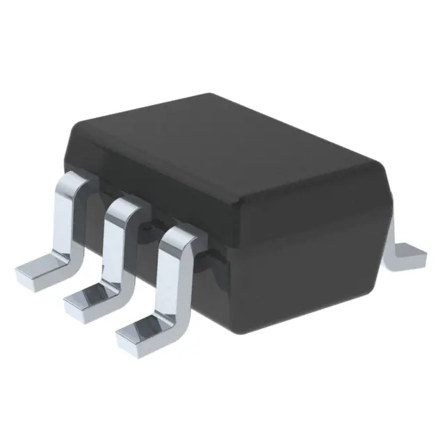
TLV61225 Single-Cell High-Efficient Step-Up Converter in 6-Pin SC-70 Package
1 Features
3 Description
•
The TLV61225 device provides a power-supply
solution for products powered by either a single-cell
or 2-cell alkaline or NiMH, or 1-cell Li-primary battery.
Possible output currents depend on the input-tooutput voltage ratio. The boost converter is based on
a hysteretic controller topology using synchronous
rectification to obtain maximum efficiency at minimal
quiescent currents. The output voltage of this device
is set internally to a fixed output voltage of 3.3 V. The
converter can be switched off by a featured enable
pin. While being switched off, battery drain is
minimized. The device is offered in a 6-pin SC-70
package (DCK) measuring 2 mm × 2 mm to enable
small circuit layout size.
1
•
•
•
•
•
•
•
•
•
Up to 94% Efficiency at Typical Operating
Conditions
5-μA Quiescent Current
Operating Input Voltage from 0.7 V to 3.3 V
Pass-Through Function During Shutdown
Output Current of More Than 40-mA From a 1.2-V
Input
Typical Switch Current Rating 400 mA
Output Overvoltage Protection
Overtemperature Protection
Fixed 3.3-V Output Voltage
Small 6-Pin SC-70 Package
Device Information(1)
2 Applications
•
•
•
PART NUMBER
TLV61225
Battery-Powered Applications
– 1- to 2- Cell NiMH or Alkaline
– 1-Cell Li-Primary
Consumer and Portable Medical Products
Personal Care Products
PACKAGE
SOT (6)
BODY SIZE (NOM)
2.00 mm × 1.25 mm
(1) For all available packages, see the orderable addendum at
the end of the data sheet.
Typical Application Schematic
L1
4.7 µH
VIN
0.8 V to VOUT
VOUT
L
VIN
C1
10 µF
FB
C2
10µF
VOUT
3.3 V
EN
GND
TLV61225
1
An IMPORTANT NOTICE at the end of this data sheet addresses availability, warranty, changes, use in safety-critical applications,
intellectual property matters and other important disclaimers. PRODUCTION DATA.
�TLV61225
SLVSAF0A – AUGUST 2010 – REVISED MAY 2015
www.ti.com
Table of Contents
1
2
3
4
5
6
7
Features ..................................................................
Applications ...........................................................
Description .............................................................
Revision History.....................................................
Pin Configuration and Functions .........................
Specifications.........................................................
1
1
1
2
3
3
6.1
6.2
6.3
6.4
6.5
6.6
6.7
3
3
3
4
4
4
5
Absolute Maximum Ratings ......................................
ESD Ratings..............................................................
Recommended Operating Conditions.......................
Thermal Information ..................................................
Electrical Characteristics...........................................
Dissipation Ratings ...................................................
Typical Characteristics ..............................................
Detailed Description .............................................. 7
7.1 Overview ................................................................... 7
7.2 Functional Block Diagram ......................................... 7
7.3 Feature Description................................................... 7
7.4 Device Functional Modes.......................................... 8
8
Application and Implementation .......................... 9
8.1 Application Information.............................................. 9
8.2 Typical Application ................................................... 9
9 Power Supply Recommendations...................... 12
10 Layout................................................................... 12
10.1 Layout Guidelines ................................................. 12
10.2 Layout Example .................................................... 12
10.3 Thermal Consideration.......................................... 13
11 Device and Documentation Support ................. 14
11.1
11.2
11.3
11.4
11.5
11.6
Device Support......................................................
Documentation Support ........................................
Community Resources..........................................
Trademarks ...........................................................
Electrostatic Discharge Caution ............................
Glossary ................................................................
14
14
14
14
14
14
12 Mechanical, Packaging, and Orderable
Information ........................................................... 14
4 Revision History
Changes from Original (August 2010) to Revision A
•
2
Page
Added Pin Configuration and Functions section, ESD Ratings table, Feature Description section, Device Functional
Modes, Application and Implementation section, Power Supply Recommendations section, Layout section, Device
and Documentation Support section, and Mechanical, Packaging, and Orderable Information section .............................. 1
Submit Documentation Feedback
Copyright © 2010–2015, Texas Instruments Incorporated
Product Folder Links: TLV61225
�TLV61225
www.ti.com
SLVSAF0A – AUGUST 2010 – REVISED MAY 2015
5 Pin Configuration and Functions
DCK Package
6-Pin SOT
(Top View)
VIN
FB
GND
EN
L
VOUT
Pin Functions
PIN
NAME
NO.
EN
6
FB
GND
I/O
DESCRIPTION
I
Enable input (1: enabled, 0: disabled). Must be actively tied high or low.
2
I
Output voltage sense input. Must be connected to VOUT.
3
—
L
5
I
Connection for Inductor
VIN
1
I
Boost converter input voltage
VOUT
4
O
Boost converter output voltage
Control / logic and power ground
6 Specifications
6.1 Absolute Maximum Ratings
over operating free-air temperature range (unless otherwise noted) (1)
MIN
Voltage
(2)
Temperature
(1)
(2)
MAX
UNIT
VIN, L, VOUT, EN, FB
–0.3
7.5
V
Operating junction temperature, TJ
–40
150
°C
Storage, Tstg
–65
150
°C
Stresses beyond those listed under Absolute Maximum Ratings may cause permanent damage to the device. These are stress ratings
only, and functional operation of the device at these or any other conditions beyond those indicated under Recommended Operating
Conditions is not implied. Exposure to absolute-maximum-rated conditions for extended periods may affect device reliability.
All voltages are with respect to network ground terminal.
6.2 ESD Ratings
VALUE
Human body model (HBM), per ANSI/ESDA/JEDEC JS-001
V(ESD)
(1)
(2)
Electrostatic discharge
(1)
UNIT
2000
Charged-device model (CDM), per JEDEC specification JESD22C101 (2)
1500
Machine model (MM)
200
V
JEDEC document JEP155 states that 500-V HBM allows safe manufacturing with a standard ESD control process.
JEDEC document JEP157 states that 250-V CDM allows safe manufacturing with a standard ESD control process.
6.3 Recommended Operating Conditions
MIN
MAX
VIN
Supply voltage at VIN
0.7
3.3
UNIT
V
TA
Operating free air temperature
–40
85
°C
TJ
Operating virtual junction temperature
–40
125
°C
Submit Documentation Feedback
Copyright © 2010–2015, Texas Instruments Incorporated
Product Folder Links: TLV61225
3
�TLV61225
SLVSAF0A – AUGUST 2010 – REVISED MAY 2015
www.ti.com
6.4 Thermal Information
TLV61225
THERMAL METRIC (1)
DCK (SOT)
UNIT
6 PINS
RθJA
Junction-to-ambient thermal resistance
231.9
°C/W
RθJC(top)
Junction-to-case (top) thermal resistance
55.8
°C/W
RθJB
Junction-to-board thermal resistance
77.3
°C/W
ψJT
Junction-to-top characterization parameter
0.7
°C/W
ψJB
Junction-to-board characterization parameter
76.4
°C/W
(1)
For more information about traditional and new thermal metrics, see the Semiconductor and IC Package Thermal Metrics application
report, SPRA953.
6.5 Electrical Characteristics
over recommended free-air temperature range and over recommended input voltage range (typical at an ambient temperature
range of 25°C) (unless otherwise noted)
PARAMETER
TEST CONDITIONS
MIN
TYP
MAX
UNIT
DC-DC STAGE
VIN
Input voltage range
VIN
Maximum minimum input voltage
RLoad ≥ 150 Ω, TA = 25°C
for start-up
VOUT
TLV61225 output voltage
ILH
Inductor current ripple
ISW
switch current limit
VOUT = 3.3 V, VIN = 1.2 V
RDSon_HSD
Rectifying switch ON-resistance
VOUT = 3.3 V
RDSon_LSD
Main switch ON-resistance
VOUT = 3.3 V
Line regulation
VIN < VOUT
0.5%
VIN < VOUT
0.5%
Load regulation
VIN
0.7
0.7
VIN < VOUT
3.13
160
Quiescent
current
ISD
Shutdown
current
ILKG_VOUT
Leakage current into VOUT
VEN = 0 V, VIN = 1.2 V, VOUT = 3.3 V
ILKG_L
Leakage current into L
VEN = 0 V, VIN = 1.2 V, VL = 1.2 V, VOUT ≥ VIN
IEN
EN input current
Clamped on GND or VIN (VIN < 1.5 V)
VIN
3.3
IO = 0 mA, VEN = VIN = 1.2 V, VOUT = 3.3 V
VEN = 0 V, VIN = 1.2 V, VOUT ≥ VIN
V
V
3.43
200
IQ
VOUT
3.3
V
mA
400
mA
1000
mΩ
600
mΩ
0.5
1
μA
5
10
μA
0.2
1
μA
μA
1
0.01
0.7
μA
0.005
0.1
μA
CONTROL STAGE
VIL
Maximum EN input low voltage
VIN ≤ 1.5 V
VIH
Minimum EN input high voltage
VIN ≤ 1.5 V
VIL
Maximum EN input low voltage
VIN > 1.5 V
VIH
Minimum EN input high voltage
VIN > 1.5 V
1.2
V
VUVLO
Undervoltage lockout threshold
for turnoff
VIN decreasing
500
mV
0.2 ×
VIN
V
0.8 ×
VIN
0.4
Undervoltage lockout hysteresis
V
50
Overvoltage protection threshold
5.5
V
mV
7.5
V
Overtemperature protection
140
°C
Overtemperature hysteresis
20
°C
6.6 Dissipation Ratings
4
PACKAGE
POWER RATING
TA ≤ 25°C
DERATING FACTOR ABOVE
TA = 25°C
DCK
444 mW
4.44 mW/°C
Submit Documentation Feedback
Copyright © 2010–2015, Texas Instruments Incorporated
Product Folder Links: TLV61225
�TLV61225
www.ti.com
SLVSAF0A – AUGUST 2010 – REVISED MAY 2015
6.7 Typical Characteristics
Table 1. Table of Graphs
FIGURE
Minimum of Maximum Output
Current
Efficiency
Input Current
Figure 1
vs Output Current, VIN = [1.2 V; 2.4 V; 3 V]
Figure 2
vs Input Voltage, IOUT = [100 uA; 1 mA; 10 mA; 50 mA]
Figure 3
vs Input Voltage at No Output Load, Device Enabled
Figure 4
vs Output Current, VIN = [1.2 V; 2.4 V]
Figure 5
vs Input Voltage, Device Disabled, RLOAD = [1 kΩ; 10 kΩ]
Figure 6
200
100
180
90
160
80
140
70
VO = 3.3 V
h - Efficiency - %
Minimum of Maximum Output Current - mA
Output Voltage
vs Input Voltage
120
100
80
VI = 3 V
60
40
30
40
20
20
10
1.0
1.2
1.4
1.6
1.8
2.0
2.2
VI - Input Voltage - V
2.4
2.6
2.8
0
0.01
3.0
0.1
Figure 1. Minimum of Maximum Output Current vs Input
Voltage
1
IO - Output Current - mA
10
100
Figure 2. Efficiency vs Output Current
100
90
VI = 2.4 V
50
60
0
0.8
VI = 1.2 V
40
IO = 10 mA
35
Device Enabled
80
30
IO = 50 mA
IO = 100 mA
II - Input Current - mA
h - Efficiency - %
70
60
50
IO = 1 mA
40
30
25
20
15
10
20
5
10
0
0.8
1.0
1.2
1.4
1.6 1.8 2.0 2.2 2.4
VI - Input Voltage - V
2.6
2.8
Figure 3. Efficiency vs Input Voltage
3.0
3.2
0
0.8
1.0
1.2
1.4
1.6 1.8 2.0 2.2 2.4
VI - Input Voltage - V
2.6
2.8
3.0
3.2
Figure 4. No Load Application Input Current vs Input
Voltage
Submit Documentation Feedback
Copyright © 2010–2015, Texas Instruments Incorporated
Product Folder Links: TLV61225
5
�TLV61225
SLVSAF0A – AUGUST 2010 – REVISED MAY 2015
www.ti.com
4.5
3.5
VEN = 0 V
VO = 3.3 V
VO - Output Voltage - V
4
VO - Output Voltage - V
3.4
VI = 2.4 V
3.3
VI = 1.2 V
3.2
3.5
3
2.5
RLOAD = 10 kW
2
1.5
RLOAD = 1 kW
1
0.5
3.1
0.01
0.1
1
IO - Output Current - mA
10
100
Figure 5. Output Voltage vs Output Current
6
0
0.7
1.2
1.7
2.2
2.7
3.2
3.7
VI - Input Voltage - V
4.2
4.7
5.2
Figure 6. Output Voltage vs Input Voltage, Device Disabled
Submit Documentation Feedback
Copyright © 2010–2015, Texas Instruments Incorporated
Product Folder Links: TLV61225
�TLV61225
www.ti.com
SLVSAF0A – AUGUST 2010 – REVISED MAY 2015
7 Detailed Description
7.1 Overview
The TLV61225 device is a high-performance, high-efficient family of switching boost converters. To achieve high
efficiency the power stage is implemented as a synchronous boost topology. Two actively controlled low RDSon
power MOSFETs are used to achieve power switching.
7.2 Functional Block Diagram
L
VOUT
VOUT
VIN
Gate
Driver
VIN
Start Up
EN
Device
Control
Current
Sensor
FB
GND
VREF
7.3 Feature Description
7.3.1
Controller Circuit
The device is controlled by a hysteretic current-mode controller. This controller regulates the output voltage by
keeping the inductor ripple current constant in the range of 200 mA and adjusting the offset of this inductor
current depending on the output load. If the required average input current is lower than the average inductor
current defined by this constant ripple, the inductor current becomes discontinuous to keep the efficiency high at
low load conditions.
IL
Continuous Current Operation
Discontinuous Current Operation
200 mA
(typ.)
200 mA
(typ.)
t
Figure 7. Hysteretic Current Operation
The output voltage VOUT is monitored through the internal feedback network, which is connected to the voltage
error amplifier. To regulate the output voltage, the voltage error amplifier compares this feedback voltage to the
internal voltage reference and adjusts the required offset of the inductor current accordingly.
Submit Documentation Feedback
Copyright © 2010–2015, Texas Instruments Incorporated
Product Folder Links: TLV61225
7
�TLV61225
SLVSAF0A – AUGUST 2010 – REVISED MAY 2015
www.ti.com
Feature Description (continued)
7.3.2 Start-Up
After the EN pin is tied high, the device starts to operate. If the input voltage is not high enough to supply the
control circuit properly, a start-up oscillator starts to operate the switches. During this phase the switching
frequency is controlled by the oscillator and the maximum switch current is limited. As soon as the device has
built up the output voltage to about 1.8 V (high enough for supplying the control circuit) the device switches to its
normal hysteretic current mode operation. The start-up time depends on input voltage, load current and output
capacitance.
7.3.3 Operation at Output Overload
If the inductor current is in normal boost operation, the current reaches the internal switch current limit threshold.
When the threshold is reached, the main switch is turned off to stop further increase of the input current.
The output voltage decreases because with limited input current is no longer possible to provide sufficient power
to the output to maintain the programmed output voltage.
If the output voltage drops below the input voltage, the back-gate diode of the rectifying switch gets forwardbiased and current starts flowing through it. This diode cannot be turned off, so the current finally is only limited
by the remaining DC resistances. As soon as the output load decreases to a value the converter can supply, the
converter resumes normal operation providing the set output voltage.
7.3.4 Undervoltage Lockout
An implemented undervoltage lockout function (UVLO) stops the operation of the converter if the input voltage
drops below the typical UVLO threshold. This function is implemented to prevent malfunctioning of the converter
and protect batteries against deep discharge.
7.3.5 Overvoltage Protection
If, for any reason, the output voltage is not fed back properly to the input of the voltage amplifier, control of the
output voltage will not work anymore. Therefore, overvoltage protection is implemented to avoid the output
voltage exceeding critical values for the device and possibly for the system it is supplying. For this protection the
TLV61225 output voltage is also monitored internally. If the output voltage of the device reaches the internally
programmed threshold, the voltage amplifier regulates the output voltage to this value.
7.3.6 Overtemperature Protection
The device has a built-in temperature sensor which monitors the internal IC junction temperature. If the
temperature exceeds the programmed threshold (see Electrical Characteristics), the device stops operating. As
soon as the IC temperature has decreased below the programmed threshold, it starts operating again. To
prevent unstable operation close to the region of overtemperature threshold, a built-in hysteresis is implemented.
7.4 Device Functional Modes
7.4.1 Device Enable and Shutdown Modes
The device is enabled when the EN pin is set high and shut down when the EN pin is low. During shutdown, the
converter stops switching and all internal control circuitry is turned off. In this case, the input voltage is connected
to the output through the back-gate diode of the rectifying MOSFET. This means that voltage will always exist at
the output, which can be as high as the input voltage or lower depending on the load.
8
Submit Documentation Feedback
Copyright © 2010–2015, Texas Instruments Incorporated
Product Folder Links: TLV61225
�TLV61225
www.ti.com
SLVSAF0A – AUGUST 2010 – REVISED MAY 2015
8 Application and Implementation
NOTE
Information in the following applications sections is not part of the TI component
specification, and TI does not warrant its accuracy or completeness. TI’s customers are
responsible for determining suitability of components for their purposes. Customers should
validate and test their design implementation to confirm system functionality.
8.1 Application Information
The TLV61225 is intended for systems which are powered by a single-cell battery to up to two Alkaline, NiCd, or
NiMH cells with a typical terminal voltage from 0.7 V to 3.3 V and can output 3.3-V voltage. Additionally, any
other voltage source with a typical output voltage from 0.7 V to 3.3 V can be used with the TLV61225.
8.2 Typical Application
L1
4.7 µH
VIN
0.8 V to VOUT
VOUT
L
VIN
C1
10 µF
FB
C2
10µF
VOUT
3.3 V
EN
GND
TLV61225
Figure 8. Typical Application Schematic
8.2.1 Design Requirements
In this example, TLV61225 is used to design a 3.3-V power supply with up to 15-mA output current capability.
The TLV61225 can be powered by a single-cell battery to up to two Alkaline, NiCd or NiMH cells with a typical
terminal voltage from 0.7 V to 3.5 V. In this example, the input voltage range is from 0.8 V to 1.5 V for single-cell
Alkaline battery input design.
Table 2. List of Components
COMPONENT
REFERENCE
PART NUMBER
MANUFACTURE
VALUE
R
C1
GRM188R60J106ME8
Murata
4D
10 μF, 6.3 V
C2
GRM188R60J106ME8
Murata
4D
10 μF, 6.3 V
L1
EPL3015-472MLB
4.7 μH
Coilcraft
8.2.2 Detailed Design Procedure
8.2.2.1 Programming the Output Voltage
At fixed voltage versions, the output voltage is programmed by an internal resistor divider. The FB pin is used to
sense the output voltage. To configure the devices properly, the FB pin must be connected directly to VOUT.
8.2.2.2 Inductor Selection
To make sure that the TLV61225 devices can operate, a suitable inductor must be connected between pin VIN
and pin L. Inductor values of 4.7 μH show good performance over the whole input and output voltage range.
Submit Documentation Feedback
Copyright © 2010–2015, Texas Instruments Incorporated
Product Folder Links: TLV61225
9
�TLV61225
SLVSAF0A – AUGUST 2010 – REVISED MAY 2015
www.ti.com
Due to the fixed inductor current ripple control the switching frequency is defined by the inductor value. For a
given switching frequency, input and output voltage the required inductance can be estimated using Equation 1.
L=
V ´ (VOUT - VIN )
1
´ IN
f ´ 200 mA
VOUT
(1)
Using inductor values greater than 4.7 μH can improve efficiency because higher values cause lower switching
frequency and less switching losses. TI does not recommend using inductor values below 2.2 μH.
To ensure reliable operation of the TLV61225 under all load conditions, TI recommends using inductors with a
current rating of 400 mA or higher. This will cover normal operation including current peaks during line and load
transients.
Table 3 lists the inductor series from different suppliers have been used with the TLV61225 converter:
Table 3. List of Inductors
VENDOR
Coilcraft
INDUCTOR SERIES
EPL3015
EPL2010
Murata
LQH3NP
Tajo Yuden
NR3015
Wurth Elektronik
WE-TPC Typ S
8.2.2.3 Capacitor Selection
8.2.2.3.1
Input Capacitor
TI recommends using at least a 10-μF input capacitor to improve transient behavior of the regulator and EMI
behavior of the total power supply circuit. TI also recommends placing a ceramic capacitor placed as close as
possible to the VIN and GND pins of the IC.
8.2.2.3.2
Output Capacitor
For the output capacitor C2 ,TI recommends using small ceramic capacitors placed as close as possible to the
VOUT and GND pins of the IC. There are no minimum output capacitor ESR requirements for maintaining control
loop stability. If the application requires the use of large capacitors which cannot be placed close to the IC, TI
recommends using a small ceramic capacitor with an capacitance value in the range of 2.2μF in parallel to the
large capacitor. Place this small capacitor as close as possible to the VOUT and GND pins of the IC.
A minimum capacitance value of 4.7 μF should be used, TI recommends using 10 μF. To calculate the required
output capacitance in case an inductor with a value higher than 4.7 μH has been selected Equation 2 can be
used.
C2 ³
10
L
´
2
(2)
Submit Documentation Feedback
Copyright © 2010–2015, Texas Instruments Incorporated
Product Folder Links: TLV61225
�TLV61225
www.ti.com
SLVSAF0A – AUGUST 2010 – REVISED MAY 2015
8.2.3 Application Curves
VI = 1.8 V, VO = 3.3 V, IO = 50 mA
IL
Icoil
Offset: 0 A
200 mA/div
50 mA/div
Offset: 0 A
IO
Offset: 0 A
20 mA/div
VO
10 mV/div
Offset: 3.31 V
Offset: 3.31 V
VO
50 mV/div
VI =1.2 V, IO = 6 mA to 50 mA
1 ms/div
200 ms/div
Figure 9. Output Voltage Ripple
Figure 10. Load Transient Response
VI = 0.9 V, VO = 3.3 V, RLOAD = 150 W
VEN
500 mV/div
VI
Icoil
200 mV/div
100 mA/div
Offset: 1.8 V
VL
2 V/div
VO
20 mV/div
Offset: 3.3 V
VO
2 V/div
VI 1.8 to 2.4 V, RLOAD = 100 W, trise = tfall = 20 ms
500 ms/div
200 ms/div
Figure 11. Line Transient Response
Figure 12. Output Voltage vs Output Current and Input
Voltage
Submit Documentation Feedback
Copyright © 2010–2015, Texas Instruments Incorporated
Product Folder Links: TLV61225
11
�TLV61225
SLVSAF0A – AUGUST 2010 – REVISED MAY 2015
www.ti.com
9 Power Supply Recommendations
The power supply can be 1-cell or 2-cell alkaline, NiCd or NiMH batteries.
The input supply should be well regulated with the rating of TLV61225. If the input supply is located more than a
few inches from the device, additional bulk capacitance may be required in addition to the ceramic bypass
capacitors. An electrolytic or tantalum capacitor with a value of 47 µF is a typical choice.
10 Layout
10.1 Layout Guidelines
As for all switching power supplies, the layout is an important step in the design, especially at high peak currents
and high switching frequencies. If the layout is not carefully done, the regulator could show stability problems as
well as EMI problems. Use wide and short traces for the main current path and for the power ground paths. The
input and output capacitor, as well as the inductor should be placed as close as possible to the IC.
To lay out the ground, TI recommended using short traces as well, separated from the power ground traces. This
avoids ground shift problems, which can occur due to superimposition of power ground current and control
ground current. Assure that the ground traces are connected close to the device GND pin.
10.2 Layout Example
L1
VOUT
Enable
VIN
C2
C1
GND
VOUT
VIN
GND
Figure 13. PCB Layout Suggestion
12
Submit Documentation Feedback
Copyright © 2010–2015, Texas Instruments Incorporated
Product Folder Links: TLV61225
�TLV61225
www.ti.com
SLVSAF0A – AUGUST 2010 – REVISED MAY 2015
10.3 Thermal Consideration
Implementation of integrated circuits in low-profile and fine-pitch surface-mount packages typically requires
special attention to power dissipation. Many system-dependent issues such as thermal coupling, airflow, added
heat sinks and convection surfaces, and the presence of other heat-generating components affect the powerdissipation limits of a given component.
Three basic approaches for enhancing thermal performance are listed below.
• Improving the power-dissipation capability of the PCB design
• Improving the thermal coupling of the component to the PCB
• Introducing airflow in the system
For more details on how to use the thermal parameters in the dissipation ratings table, check the Thermal
Characteristics Application Note (SZZA017) and the Semiconductor and IC Package Thermal Metrics Application
Note (SPRA953).
Submit Documentation Feedback
Copyright © 2010–2015, Texas Instruments Incorporated
Product Folder Links: TLV61225
13
�TLV61225
SLVSAF0A – AUGUST 2010 – REVISED MAY 2015
www.ti.com
11 Device and Documentation Support
11.1 Device Support
11.1.1 Third-Party Products Disclaimer
TI'S PUBLICATION OF INFORMATION REGARDING THIRD-PARTY PRODUCTS OR SERVICES DOES NOT
CONSTITUTE AN ENDORSEMENT REGARDING THE SUITABILITY OF SUCH PRODUCTS OR SERVICES
OR A WARRANTY, REPRESENTATION OR ENDORSEMENT OF SUCH PRODUCTS OR SERVICES, EITHER
ALONE OR IN COMBINATION WITH ANY TI PRODUCT OR SERVICE.
11.2 Documentation Support
11.2.1 Related Documentation
For related documentation, see the following:
• Thermal Characteristics Application Note, SZZA017
11.3 Community Resources
The following links connect to TI community resources. Linked contents are provided "AS IS" by the respective
contributors. They do not constitute TI specifications and do not necessarily reflect TI's views; see TI's Terms of
Use.
TI E2E™ Online Community TI's Engineer-to-Engineer (E2E) Community. Created to foster collaboration
among engineers. At e2e.ti.com, you can ask questions, share knowledge, explore ideas and help
solve problems with fellow engineers.
Design Support TI's Design Support Quickly find helpful E2E forums along with design support tools and
contact information for technical support.
11.4 Trademarks
E2E is a trademark of Texas Instruments.
All other trademarks are the property of their respective owners.
11.5 Electrostatic Discharge Caution
These devices have limited built-in ESD protection. The leads should be shorted together or the device placed in conductive foam
during storage or handling to prevent electrostatic damage to the MOS gates.
11.6 Glossary
SLYZ022 — TI Glossary.
This glossary lists and explains terms, acronyms, and definitions.
12 Mechanical, Packaging, and Orderable Information
The following pages include mechanical, packaging, and orderable information. This information is the most
current data available for the designated devices. This data is subject to change without notice and revision of
this document. For browser-based versions of this data sheet, refer to the left-hand navigation.
14
Submit Documentation Feedback
Copyright © 2010–2015, Texas Instruments Incorporated
Product Folder Links: TLV61225
�PACKAGE OPTION ADDENDUM
www.ti.com
10-Dec-2020
PACKAGING INFORMATION
Orderable Device
Status
(1)
Package Type Package Pins Package
Drawing
Qty
Eco Plan
(2)
Lead finish/
Ball material
MSL Peak Temp
Op Temp (°C)
Device Marking
(3)
(4/5)
(6)
TLV61225DCKR
ACTIVE
SC70
DCK
6
3000
RoHS & Green
NIPDAU
Level-1-260C-UNLIM
-40 to 85
QUL
TLV61225DCKT
ACTIVE
SC70
DCK
6
250
RoHS & Green
NIPDAU
Level-1-260C-UNLIM
-40 to 85
QUL
(1)
The marketing status values are defined as follows:
ACTIVE: Product device recommended for new designs.
LIFEBUY: TI has announced that the device will be discontinued, and a lifetime-buy period is in effect.
NRND: Not recommended for new designs. Device is in production to support existing customers, but TI does not recommend using this part in a new design.
PREVIEW: Device has been announced but is not in production. Samples may or may not be available.
OBSOLETE: TI has discontinued the production of the device.
(2)
RoHS: TI defines "RoHS" to mean semiconductor products that are compliant with the current EU RoHS requirements for all 10 RoHS substances, including the requirement that RoHS substance
do not exceed 0.1% by weight in homogeneous materials. Where designed to be soldered at high temperatures, "RoHS" products are suitable for use in specified lead-free processes. TI may
reference these types of products as "Pb-Free".
RoHS Exempt: TI defines "RoHS Exempt" to mean products that contain lead but are compliant with EU RoHS pursuant to a specific EU RoHS exemption.
Green: TI defines "Green" to mean the content of Chlorine (Cl) and Bromine (Br) based flame retardants meet JS709B low halogen requirements of


 工商网监
湘ICP备2023018690号
工商网监
湘ICP备2023018690号
