TLV733P-Q1
SBVS283F – AUGUST 2016 – REVISED TLV733P-Q1
OCTOBER 2020
SBVS283F – AUGUST 2016 – REVISED OCTOBER 2020
www.ti.com
TLV733P-Q1
Capacitor-Free, 300-mA, Low Dropout (LDO) Linear Regulator
1 Features
3 Description
•
The TLV733P-Q1 family of low dropout (LDO) linear
regulators are ultra-small, low quiescent current LDOs
that can source 300 mA with good line and load
transient performance. These devices provide a
typical accuracy of 1%.
•
•
•
•
•
•
•
•
•
•
•
AEC-Q100 qualified for automotive applications:
– Temperature grade 1: –40°C to 125°C, TA
Device junction temperature range:
–40°C to 150°C
Input voltage range: 1.4 V to 5.5 V
Stable operation with or without capacitors
Foldback overcurrent protection
Package:
– 2.0-mm × 2.0-mm WSON-6
– 2.9-mm × 1.6-mm SOT-23
Very low dropout: 125 mV at 300 mA (3.3 VOUT)
Accuracy: 1% typical, 1.4% maximum
Low IQ: 34 µA
Available in fixed-output voltages:
1.0 V to 3.3 V
High PSRR: 50 dB at 1 kHz
Active output discharge
2 Applications
•
•
•
The TLV733P-Q1 family is designed with a modern
capacitor-free architecture to ensure stability without
an input or output capacitor. The removal of the output
capacitor allows for a very small solution size, and
can eliminate inrush current at startup. Furthermore,
the TLV733P-Q1 family is also stable with ceramic
output capacitors if an output capacitor is necessary.
The TLV733P-Q1 family also provides foldback
current control during device power-up and enabling if
an output capacitor is used. This functionality is
especially important in battery-operated devices.
The TLV733P-Q1 family provides an active pulldown
circuit to quickly discharge output loads when
disabled.
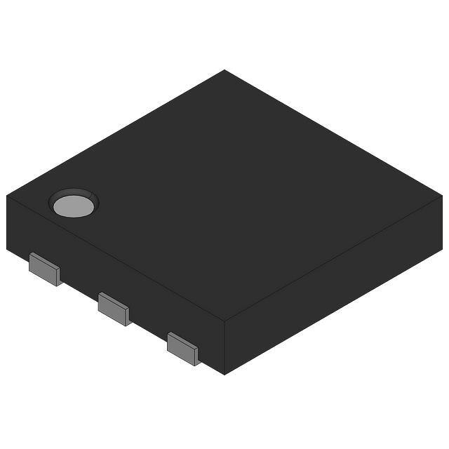
The TLV733P-Q1 family is available in the 6-pin DRV
(WSON) and 5-pin DBV (SOT-23) packages.
Camera modules
Automotive infotainment
Navigation systems
Device Information (1)
PART NUMBER
TLV733P-Q1
(1)
PACKAGE
BODY SIZE (NOM)
WSON (6)
2.00 mm × 2.00 mm
SOT-23 (5)
2.90 mm × 1.60 mm
For all available packages, see the package option
addendum at the end of the data sheet.
180
OUT
EN
Optional
140
COUT
TLV733P-Q1
CIN
VOUT = 3.3 V
VOUT = 1.8 V
160
GND
Optional
ON
OFF
Typical Application Circuit
120
VDO (mV)
IN
100
80
60
40
20
0
0
30
60
90
120 150 180
IOUT (mA)
210
240
270
300
D020
Dropout Voltage vs Output Current
An IMPORTANT NOTICE at the end of this data sheet addresses availability, warranty, changes, use in safety-critical applications,
Submit Document Feedback
Copyright
© 2020 Texas
Instruments
Incorporated
intellectual
property
matters
and other important disclaimers. PRODUCTION DATA.
Product Folder Links: TLV733P-Q1
1
�TLV733P-Q1
www.ti.com
SBVS283F – AUGUST 2016 – REVISED OCTOBER 2020
Table of Contents
1 Features............................................................................1
2 Applications..................................................................... 1
3 Description.......................................................................1
4 Revision History.............................................................. 2
5 Pin Configuration and Functions...................................4
6 Specifications.................................................................. 5
6.1 Absolute Maximum Ratings........................................ 5
6.2 ESD Ratings............................................................... 5
6.3 Recommended Operating Conditions.........................5
6.4 Thermal Information....................................................5
6.5 Electrical Characteristics.............................................6
6.6 Timing Requirements.................................................. 7
6.7 Typical Characteristics................................................ 8
7 Detailed Description......................................................12
7.1 Overview................................................................... 12
7.2 Functional Block Diagram......................................... 12
7.3 Feature Description...................................................13
7.4 Device Functional Modes..........................................14
8 Application and Implementation.................................. 15
8.1 Application Information............................................. 15
8.2 Typical Applications.................................................. 16
9 Layout.............................................................................18
9.1 Layout Guidelines..................................................... 18
9.2 Layout Examples...................................................... 18
10 Device and Documentation Support..........................19
10.1 Device Support....................................................... 19
10.2 Receiving Notification of Documentation Updates..19
10.3 Support Resources................................................. 19
10.4 Trademarks............................................................. 19
10.5 Electrostatic Discharge Caution..............................19
10.6 Glossary..................................................................19
4 Revision History
NOTE: Page numbers for previous revisions may differ from page numbers in the current version.
Changes from Revision E (July 2019) to Revision F (October 2020)
Page
• Updated the numbering format for tables and figures throughout the document............................................... 1
• Changed automotive-specific Features bullets...................................................................................................1
• Changed storage temperature max parameter from 160°C to 150°C................................................................ 5
• Added classificaton levels to ESD Ratings table................................................................................................ 5
Changes from Revision D (December 2018) to Revision E (July 2019)
Page
• Changed description of EN pin in Pin Functions table........................................................................................4
• Deleted typical specifications from VEN(HI) and VEN(LO) parameters in Electrical Characteristics table.............. 6
• Added maximum specification to ILIM parameter in Electrical Characteristics table........................................... 6
• Added and Output Enable to title and changed first paragraph of Shutdown and Output Enable section....... 13
Changes from Revision C (October 2018) to Revision D (December 2018)
Page
• Changed status of DBV package to Production Data ........................................................................................1
Changes from Revision B (August 2018) to Revision C (October 2018)
Page
• Added DBV package to document as Preview................................................................................................... 1
Changes from Revision A (August 2016) to Revision B (August 2018)
Page
• Added Device Junction Temperature Range Features bullet ............................................................................ 1
• Changed TJ maximum specification from 135°C to 150°C ................................................................................ 5
• Changed Electrical Characteristics conditions statement from TJ, TA = –40°C to +125°C to TJ = –40°C to
+150°C, TA = –40°C to +125°C ......................................................................................................................... 6
• Added last 6 rows to VDO parameter ................................................................................................................. 6
• Added second row to IGND parameter, added temperature range to first row test conditions ..........................6
• Changed Typical Characteristics condition statement from TJ = –40°C to +125°C to TJ = –40°C to +150°C ....
8
• Changed operating junction temperature from –40°C to +135°C to –40°C to +150°C in Overview section.....12
• Changed junction temperature limit from 135°C to 150°C in Thermal Shutdown section................................ 13
2
Submit Document Feedback
Copyright © 2020 Texas Instruments Incorporated
Product Folder Links: TLV733P-Q1
�TLV733P-Q1
www.ti.com
SBVS283F – AUGUST 2016 – REVISED OCTOBER 2020
Changes from Revision * (August 2016) to Revision A (August 2016)
Page
• Released to production ......................................................................................................................................1
Submit Document Feedback
Copyright © 2020 Texas Instruments Incorporated
Product Folder Links: TLV733P-Q1
3
�TLV733P-Q1
www.ti.com
SBVS283F – AUGUST 2016 – REVISED OCTOBER 2020
5 Pin Configuration and Functions
OUT
1
NC
2
GND
3
GND
6
IN
5
NC
4
EN
IN
1
GND
2
EN
3
5
OUT
4
NC
Not to scale
Not to scale
NC – No internal connection.
Figure 5-1. DRV Package, 6-Pin WSON, Top View
Figure 5-2. DBV Package, 5-Pin SOT-23, Top View
Table 5-1. Pin Functions
NO.
NAME
DBV
I/O
DESCRIPTION
Enable pin. Drive EN greater than VEN(HI) to turn on the regulator.
Drive EN less than VEN(LO) to put the LDO into shutdown mode.
EN
4
3
I
GND
3
2
—
IN
6
1
I
NC
2, 5
4
—
No internal connection
1
5
O
Regulated output voltage pin. For best transient response, use a small 1-μF ceramic
capacitor from this pin to ground. See the Input and Output Capacitor Selection section for
more details.
—
—
The thermal pad is electrically connected to the GND node.
Connect to the GND plane for improved thermal performance.
OUT
Thermal pad
4
DRV
Ground pin
Input pin. A small capacitor is recommended from this pin to ground.
See the Input and Output Capacitor Selection section for more details.
Submit Document Feedback
Copyright © 2020 Texas Instruments Incorporated
Product Folder Links: TLV733P-Q1
�TLV733P-Q1
www.ti.com
SBVS283F – AUGUST 2016 – REVISED OCTOBER 2020
6 Specifications
6.1 Absolute Maximum Ratings
over operating junction temperature range (unless otherwise noted); all voltages are with respect to GND(1)
Voltage
Current
MIN
MAX
VIN
–0.3
6.0
VEN
–0.3
VIN + 0.3
VOUT
–0.3
3.6
IOUT
(1)
V
Internally limited
Output short-circuit duration
Temperature
UNIT
A
Indefinite
Operating junction, TJ
–40
150
Storage, Tstg
–65
150
°C
Stresses beyond those listed under Absolute Maximum Ratings may cause permanent damage to the device. These are stress ratings
only, which do not imply functional operation of the device at these or any other conditions beyond those indicated under
Recommended Operating Conditions. Exposure to absolute-maximum-rated conditions for extended periods may affect device
reliability.
6.2 ESD Ratings
VALUE
Human-body model (HBM), per AEC Q100-002(1), classification level 2
V(ESD)
(1)
Electrostatic
discharge
Charged-device model (CDM), per AEC Q100-011,
classification level C4B
UNIT
±2000
All pins
±500
Corner pins (1, 3, 4, and 6)
±750
V
AEC Q100-002 indicates that HBM stressing shall be in accordance with the ANSI/ESDA/JEDEC JS-001 specification.
6.3 Recommended Operating Conditions
over operating junction temperature range (unless otherwise noted)
MIN
NOM
MAX
5.5
UNIT
VIN
Input range
1.4
V
VOUT
Output range
1.0
3.3
V
IOUT
Output current
0
300
mA
VEN
Enable range
0
VIN
V
TJ
Junction temperature
–40
150
°C
TA
Ambient temperature
–40
125
°C
6.4 Thermal Information
TLV733P-Q1
THERMAL METRIC(1)
DRV (WSON)
DBV (SOT-23)
UNIT
6 PINS
5 PINS
RθJA
Junction-to-ambient thermal resistance
92.5
198.3
°C/W
RθJC(top)
Junction-to-case (top) thermal resistance
123.9
118.4
°C/W
RθJB
Junction-to-board thermal resistance
61.9
65.8
°C/W
ψJT
Junction-to-top characterization parameter
9.7
42.4
°C/W
ψJB
Junction-to-board characterization parameter
62.3
65.5
°C/W
RθJC(bot)
Junction-to-case (bottom) thermal resistance
30.9
n/a
°C/W
(1)
For more information about traditional and new thermal metrics, see the Semiconductor and IC Package Thermal Metrics application
report.
Submit Document Feedback
Copyright © 2020 Texas Instruments Incorporated
Product Folder Links: TLV733P-Q1
5
�TLV733P-Q1
www.ti.com
SBVS283F – AUGUST 2016 – REVISED OCTOBER 2020
6.5 Electrical Characteristics
at operating temperature range (TJ = –40°C to +150°C, TA = –40°C to +125°C), VIN = VOUT(nom) + 0.5 V or 2.0 V
(whichever is greater), IOUT = 1 mA, VEN = VIN, and CIN = COUT = 1 µF (unless otherwise noted); all typical
values are at TJ = 25°C
PARAMETER
VIN
TEST CONDITIONS
Input voltage
DC output accuracy
TJ = 25°C
–40°C ≤ TJ ≤ 150°C
1.4
5.5
1%
–1.4%
1.25
Line regulation
ΔVI = VOUT(nom) + 0.5 V or 2.0 V (whichever is greater) to
5.5 V
ΔVO(ΔIO)
Load regulation
ΔIO = 1 mA to 300 mA
VOUT = 0.98 ×
VOUT(nom),
IOUT = 300 mA
25
1.2 V ≤ VOUT < 1.5 V, –40°C ≤ TJ ≤ 125°C
450
1.5 V ≤ VOUT < 1.8 V, –40°C ≤ TJ ≤ 125°C
400
1.8 V ≤ VOUT < 2.5 V, –40°C ≤ TJ ≤ 125°C
300
2.5 V ≤ VOUT < 3.3 V, –40°C ≤ TJ ≤ 125°C
290
125
560
1.2 V ≤ VOUT < 1.5 V, –40°C ≤ TJ ≤ 150°C
490
1.5 V ≤ VOUT < 1.8 V, –40°C ≤ TJ ≤ 150°C
440
1.8 V ≤ VOUT < 2.5 V, –40°C ≤ TJ ≤ 150°C
340
2.5 V ≤ VOUT < 3.3 V, –40°C ≤ TJ ≤ 150°C
330
VEN ≤ 0.35 V, 2.0 V ≤ VIN ≤ 5.5 V, TJ = 25°C
0.1
f = 100 Hz
68
PSRR
Power-supply
rejection ratio
VOUT = 1.8 V,
IOUT = 300 mA
f = 10 kHz
35
Vn
Output noise voltage
BW = 10 Hz to 100 kHz, VOUT = 1.8 V, IOUT = 10 mA
VEN(HI)
EN pin high voltage
(enabled)
VEN(LO)
EN pin low voltage
(disabled)
IEN
EN pin current
VEN = 5.5 V
Pulldown resistor
VIN = 2.3 V
Thermal shutdown
(1)
6
34
Shutdown current
Tsd
mV
320
IOUT = 0 mA, –40°C ≤ TJ ≤ 125°C
ISHDN
Short-circuit current
limit
270
VOUT = 1.1 V, –40°C ≤ TJ ≤ 150°C
Ground pin current
IOS
V
mV
510
IGND
Output current limit
V
mV
VOUT = 1.1 V, –40°C ≤ TJ ≤ +125°C
VOUT = 3.3 V, –40°C ≤ TJ ≤ 150°C
ILIM
1.4
1
VOUT = 3.3 V, –40°C ≤ TJ ≤ 125°C
UNIT
1.4%
VIN falling
ΔVO(ΔVI)
MAX
–1%
1.3
Undervoltage lockout
Dropout voltage(1)
TYP
VIN rising
UVLO
VDO
MIN
IOUT = 0 mA, –40°C ≤ TJ ≤ 150°C
62
78
f = 100 kHz
1
µA
µA
dB
28
120
µVRMS
0.9
V
0.35
0.01
µA
120
360
Ω
700
VOUT shorted to GND, VOUT = 1.0 V
150
VOUT shorted to GND, VOUT = 3.3 V
170
Shutdown, temperature increasing
160
Reset, temperature decreasing
140
V
mA
mA
°C
Dropout voltage for the TLV73310P is not valid at room temperature. The device engages undervoltage lockout (VIN < UVLOFALL)
before the dropout condition is met.
Submit Document Feedback
Copyright © 2020 Texas Instruments Incorporated
Product Folder Links: TLV733P-Q1
�TLV733P-Q1
www.ti.com
SBVS283F – AUGUST 2016 – REVISED OCTOBER 2020
6.6 Timing Requirements
MIN
tSTR
Startup time
NOM
Time from EN assertion to 98% × VOUT(nom), VOUT = 1.0 V, IOUT = 0 mA
250
Time from EN assertion to 98% × VOUT(nom), VOUT = 3.3 V, IOUT = 0 mA
800
MAX UNIT
µs
Submit Document Feedback
Copyright © 2020 Texas Instruments Incorporated
Product Folder Links: TLV733P-Q1
7
�TLV733P-Q1
www.ti.com
SBVS283F – AUGUST 2016 – REVISED OCTOBER 2020
6.7 Typical Characteristics
at operating temperature range (TJ = –40°C to +150°C), VIN = VOUT(nom) + 0.5 V or 2.0 V (whichever is greater),
IOUT = 1 mA, VEN = VIN, and CIN = COUT = 1 µF (unless otherwise noted)
70
1.816
TJ = -40qC
TJ = 0qC
TJ = 25qC
TJ = 85qC
TJ = 125qC
1.814
1.812
60
55
1.808
IGND (PA)
VOUT (V)
1.81
TJ = -40qC
TJ = 0qC
TJ = 25qC
TJ = 85qC
TJ = 125qC
65
1.806
1.804
50
45
40
1.802
1.8
35
1.798
30
1.796
25
2
2.5
3
3.5
4
VIN (V)
4.5
5
5.5
0
30
Figure 6-1. 1.8-V Regulation vs VIN (Line
Regulation) and Temperature
90
120 150 180
IOUT (mA)
210
240
270
300
D012
Figure 6-2. Ground Pin Current vs IOUT and
Temperature
40
100
TJ = 25qC
TJ = -40qC
TJ = 0qC
TJ = 25qC
TJ = 85qC
TJ = 125qC
35
30
10
25
ISHDN (PA)
IGND (PA)
60
D019
20
15
1
10
0.1
5
0
0.5
0.01
1
1.5
2
2.5
3
3.5
VIN (V)
4
4.5
5
5.5
0
D013
1
2
3
VIN (V)
4
5
6
D015
IOUT = 0 mA
Figure 6-3. Ground Pin Current vs VIN
Figure 6-4. Shutdown Current vs VIN and
Temperature
0.675
1
VEN(LO)
VEN(HI)
0.9
0.625
0.8
0.6
0.7
0.575
0.6
VOUT (V)
Enable Threshold (V)
0.65
0.55
0.525
0.4
0.5
0.3
0.475
0.2
0.45
0.1
0.425
-40
-20
0
20
40
60
TJ (qC)
80
100
120
140
D014
Figure 6-5. Enable Threshold vs Temperature
8
0.5
TJ = -40°C
TJ = 0°C
TJ = 25°C
TJ = 85°C
TJ = 125°C
0
150 200 250 300 350 400 450 500 550 600 650 700
Output Current (mA)
D023
Figure 6-6. Output Voltage vs 1.0-V Foldback
Current Limit and Temperature
Submit Document Feedback
Copyright © 2020 Texas Instruments Incorporated
Product Folder Links: TLV733P-Q1
�TLV733P-Q1
www.ti.com
SBVS283F – AUGUST 2016 – REVISED OCTOBER 2020
2
3.5
1.75
3
2.5
1.25
VOUT (V)
VOUT (V)
1.5
1
0.75
TJ = -40°C
TJ = 0°C
TJ = 25°C
TJ = 85°C
TJ = 125°C
0.5
0.25
0
150
200
250
300
350
400
Output Current (mA)
450
TJ = -40°C
TJ = 0°C
TJ = 25°C
TJ = 85°C
TJ = 125°C
0.5
0
150
500
D021
200
250
300
350
400
Output Current (mA)
450
500
D022
Figure 6-8. Output Voltage vs 3.3-V Foldback
Current Limit and Temperature
80
10
VOUT = 1 V
VOUT = 1.8 V
VOUT = 3.3 V
No Output Capacitor
1-PF Output Capacitor
Noise Density (PV/—Hz)
70
60
PSRR (dB)
1.5
1
Figure 6-7. Output Voltage vs 1.8-V Foldback
Current Limit and Temperature
50
40
30
20
1
0.1
0.01
10
0
10
2
100
1k
10k
Frequency (Hz)
100k
1M
0.005
10
100
D017
100k
1M
D016
IOUT = 300 mA
IOUT = 300 mA
Figure 6-9. Power-Supply Rejection Ratio vs
Frequency
1k
10k
Frequency (Hz)
Figure 6-10. Output Spectral Noise Density vs
Frequency and Output Voltage
VIN (2 V/div)
VIN (2 V/div)
VOUT (1 V/div,
AC Coupled)
VOUT (1 V/div,
AC Coupled)
Time (20 µs/div)
Time (20 µs/div)
IOUT = 10 mA, 1-µF output capacitor
IOUT = 300 mA, 1-µF output capacitor
Figure 6-11. Line Transient
Figure 6-12. Line Transient
Submit Document Feedback
Copyright © 2020 Texas Instruments Incorporated
Product Folder Links: TLV733P-Q1
9
�TLV733P-Q1
www.ti.com
SBVS283F – AUGUST 2016 – REVISED OCTOBER 2020
VOUT (200 mV/div,
AC Coupled)
VOUT (200 mV/div,
AC Coupled)
ILOAD (100 mA/div)
ILOAD (100 mA/div)
Time (20 µs/div)
Time (20 µs/div)
VIN = 2.0 V, 1-µF output capacitor, output current slew rate =
0.25 A/µs
Figure 6-13. 1.0-V, 50-mA to 300-mA Load
Transient
VIN = 2.0 V, no output capacitor, output current slew rate =
0.25 A/µs
Figure 6-14. 1.0 V, 50-mA to 300-mA Load Transient
VOUT (100 mV/div,
AC Coupled)
VOUT (100 mV/div,
AC coupled)
ILOAD (100 mA/div)
ILOAD (200 mA/div)
Time (20 µs/div)
Time (50 µs/div)
VIN = 3.8 V,1-µF output capacitor, output current slew rate =
0.25 A/µs
VIN = 3.8 V, no output capacitor, output current slew rate =
0.25 A/µs
Figure 6-15. 3.3 V, 50-mA to 300-mA Load Transient Figure 6-16. 3.3 V, 50-mA to 300-mA Load Transient
VEN (500 mV/div)
VIN (1 V/div)
VOUT (1 V/div)
ILOAD (200 mA/div)
VOUT (500 mV/div)
Time (100 µs/div)
Time (100 µs/div)
RL = 6.2 Ω, VEN = VIN, 1-µF output capacitor
Figure 6-17. VIN Power-Up and Power-Down
10
RL = 6.2 Ω, 1-µF output capacitor
Figure 6-18. Startup with EN
Submit Document Feedback
Copyright © 2020 Texas Instruments Incorporated
Product Folder Links: TLV733P-Q1
�TLV733P-Q1
www.ti.com
SBVS283F – AUGUST 2016 – REVISED OCTOBER 2020
VOUT (500 mV/div)
VEN (500 mV/div)
VOUT (500 mV/div)
ILOAD (200 mA/div)
Time (100 µs/div)
Time (100 µs/div)
1-µF output capacitor
IOUT = 300 mA, 1-µF output capacitor
Figure 6-19. Shutdown Response with Enable
Figure 6-20. Foldback Current Limit Response
Submit Document Feedback
Copyright © 2020 Texas Instruments Incorporated
Product Folder Links: TLV733P-Q1
11
�TLV733P-Q1
www.ti.com
SBVS283F – AUGUST 2016 – REVISED OCTOBER 2020
7 Detailed Description
7.1 Overview
The TLV733P-Q1 belongs to a family of low dropout (LDO) linear regulators. These devices consume low
quiescent current and deliver excellent line and load transient performance. These characteristics, combined
with low noise and good PSRR with low dropout voltage, make this family of devices ideal for portable consumer
applications.
This family of regulators offers foldback current limit, shutdown, and thermal protection. The operating junction
temperature for this family of devices is –40°C to +150°C.
7.2 Functional Block Diagram
IN
OUT
Current
Limit
Thermal
Shutdown
UVLO
EN
120 W
Band Gap
Logic
TLV733P-Q1
GND
12
Submit Document Feedback
Copyright © 2020 Texas Instruments Incorporated
Product Folder Links: TLV733P-Q1
�TLV733P-Q1
www.ti.com
SBVS283F – AUGUST 2016 – REVISED OCTOBER 2020
7.3 Feature Description
7.3.1 Undervoltage Lockout (UVLO)
The TLV733P-Q1 family uses an undervoltage lockout (UVLO) circuit that disables the output until the input
voltage is greater than the rising UVLO voltage. This circuit ensures that the device does not exhibit any
unpredictable behavior when the supply voltage is lower than the operational range of the internal circuitry.
During UVLO disable, the output is connected to ground with a 120-Ω pulldown resistor.
7.3.2 Shutdown and Output Enable
The enable pin (EN) is active high. Enable the device by forcing the EN pin to exceed VEN(HI). Turn off the device
by forcing the EN pin to drop below VEN(LO). If shutdown capability is not required, connect EN to IN. There is no
internal pulldown resistor connected to the EN pin.
The TLV733P-Q1 has an internal pulldown MOSFET that connects a 120-Ω resistor to ground when the device
is disabled. The discharge time after disabling depends on the output capacitance (COUT) and the load
resistance (RL) in parallel with the 120-Ω pulldown resistor. The time constant is calculated in Equation 1:
t=
120 · RL
120 + RL
· COUT
(1)
7.3.3 Internal Foldback Current Limit
The TLV733P-Q1 has an internal foldback current limit that protects the regulator during fault conditions. The
current allowed through the device is reduced when the output voltage falls. When the output is shorted, the
LDO supplies a typical current of 150 mA. The output voltage is not regulated when the device is in current limit.
In this condition, the output voltage is the product of the regulated current and the load resistance. When the
device output is shorted, the PMOS pass transistor dissipates power [(VIN – V OUT) × IOS] until thermal shutdown
is triggered and the device turns off. After the device cools down, the internal thermal shutdown circuit turns the
device back on. If the fault condition continues, the device cycles between current limit and thermal shutdown;
see the Thermal Information table for more details.
The foldback current-limit circuit limits the current allowed through the device to current levels lower than the
minimum current limit at a nominal VOUT current limit (ILIM) during startup. See Figure 6-6 to Figure 6-8 for typical
foldback current limit values. If the output is loaded by a constant-current load during startup, or if the output
voltage is negative when the device is enabled, then the load current demanded by the load can exceed the
foldback current limit and the device may not rise to the full output voltage. For constant-current loads, disable
the output load until the TLV733P-Q1 has fully risen to the nominal output voltage.
The TLV733P-Q1 PMOS pass element has an intrinsic body diode that conducts current when the voltage at the
OUT pin exceeds the voltage at the IN pin. Do not force the output voltage to exceed the input voltage because
excessively high current can flow through the body diode.
7.3.4 Thermal Shutdown
Thermal shutdown protection disables the output when the junction temperature rises to approximately 160°C.
Disabling the device eliminates the power dissipated by the device, allowing the device to cool. When the
junction temperature cools to approximately 140°C, the output circuitry is again enabled. Depending on power
dissipation, thermal resistance, and ambient temperature, the thermal protection circuit can cycle on and off.
This cycling limits regulator dissipation, protecting the device from damage as a result of overheating.
Activating the thermal shutdown feature usually indicates excessive power dissipation as a result of the product
of the (VIN – VOUT) voltage and the load current. For reliable operation, limit junction temperature to 150°C
(maximum). To estimate the margin of safety in a complete design, increase the ambient temperature until the
thermal protection is triggered; use worst-case loads and signal conditions.
The TLV733P-Q1 internal protection circuitry protects against overload conditions but is not intended to be
activated in normal operation. Continuously running the TLV733P-Q1 into thermal shutdown degrades device
reliability.
Submit Document Feedback
Copyright © 2020 Texas Instruments Incorporated
Product Folder Links: TLV733P-Q1
13
�TLV733P-Q1
www.ti.com
SBVS283F – AUGUST 2016 – REVISED OCTOBER 2020
7.4 Device Functional Modes
7.4.1 Normal Operation
The device regulates to the nominal output voltage under the following conditions:
•
•
•
•
•
The input voltage has previously exceeded the UVLO rising voltage and has not decreased below the UVLO
falling threshold.
The input voltage is greater than the nominal output voltage added to the dropout voltage.
The enable voltage has previously exceeded the enable rising threshold voltage and has not decreased
below the enable falling threshold.
The output current is less than the current limit.
The device junction temperature is less than the thermal shutdown temperature.
7.4.2 Dropout Operation
If the input voltage is lower than the nominal output voltage plus the specified dropout voltage, but all other
conditions are met for normal operation, the device operates in dropout mode. In this condition, the output
voltage is the same as the input voltage minus the dropout voltage. The transient performance of the device is
significantly degraded because the pass device is in a triode state and no longer controls the current through the
LDO. Line or load transients in dropout can result in large output voltage deviations.
7.4.3 Disabled
The device is disabled under the following conditions:
•
•
•
The input voltage is less than the UVLO falling voltage, or has not yet exceeded the UVLO rising threshold.
The enable voltage is less than the enable falling threshold voltage or has not yet exceeded the enable rising
threshold.
The device junction temperature is greater than the thermal shutdown temperature.
When the device is disabled, the active pulldown resistor discharges the output.
Table 7-1 shows the conditions that lead to the different modes of operation.
Table 7-1. Device Functional Mode Comparison
PARAMETER
OPERATING MODE
VIN
VEN
IOUT
TJ
Normal mode
VIN > VOUT(nom) + VDO
and VIN > UVLORISE
VEN > VEN(HI)
IOUT < ILIM
TJ < 160°C
Dropout mode
UVLORISE < VIN < VOUT(nom) + VDO
VEN > VEN(HI)
IOUT < ILIM
TJ < 160°C
VIN < UVLOFALL
VEN < VEN(LO)
—
TJ > 160°C
Disabled mode
(any true condition
disables the device)
14
Submit Document Feedback
Copyright © 2020 Texas Instruments Incorporated
Product Folder Links: TLV733P-Q1
�TLV733P-Q1
www.ti.com
SBVS283F – AUGUST 2016 – REVISED OCTOBER 2020
8 Application and Implementation
Note
Information in the following applications sections is not part of the TI component specification, and TI
does not warrant its accuracy or completeness. TI’s customers are responsible for determining
suitability of components for their purposes. Customers should validate and test their design
implementation to confirm system functionality.
8.1 Application Information
8.1.1 Input and Output Capacitor Selection
The TLV733P-Q1 uses an advanced internal control loop to obtain stable operation both with and without the
use of input or output capacitors. Dynamic performance is improved with the use of an output capacitor, and can
be improved with an input capacitor. An output capacitance of 0.1 μF or larger generally provides good dynamic
response. Use X5R- and X7R-type ceramic capacitors because these capacitors have minimal variation in value
and equivalent series resistance (ESR) over temperature.
Although an input capacitor is not required for stability, increased output impedance from the input supply can
compromise the performance of the TLV733P-Q1. Good analog design practice is to connect a 0.1-µF to 1-µF
capacitor from IN to GND. This capacitor counteracts reactive input sources and improves transient response,
input ripple, and PSRR. Use an input capacitor if the source impedance is greater than 0.5 Ω. Use a highervalue capacitor if large, fast rise-time load transients are anticipated, or if the device is located several inches
from the input power source.
Figure 8-1 shows the transient performance improvements with an external 1-µF capacitor on the output versus
no output capacitor. The data in this figure are taken with an increasing load step from 50 mA to 300 mA, and
the peak output voltage deviation (load transient response) is measured. For low output current slew rates,
(< 0.1 A/µs), the transient performance of the device is similar with or without an output capacitor. When the
current slew rate is increased, the peak voltage deviation is significantly increased. For loads that exhibit fast
current slew rates above 0.1 A/µs, use an output capacitor. For best performance, the maximum recommended
output capacitance is 100 µF.
Peak Output Voltage Change (%VOUT)
35
30
1-PF COUT
COUT Removed
25
20
15
10
5
0
0.01
0.1
Output Load Transient Slew Rate (A/Ps)
1
D027
Output current stepped from 50 mA to 300 mA, output voltage change measured at positive dI/dt
Figure 8-1. Output Voltage Deviation vs Load Step Slew Rate
Some applications benefit from the removal of the output capacitor. In addition to space and cost savings, the
removal of the output capacitor lowers inrush current as a result of eliminating the required current flow into the
output capacitor at startup. In these cases, take care to ensure that the load is tolerant of the additional output
voltage deviations.
Submit Document Feedback
Copyright © 2020 Texas Instruments Incorporated
Product Folder Links: TLV733P-Q1
15
�TLV733P-Q1
www.ti.com
SBVS283F – AUGUST 2016 – REVISED OCTOBER 2020
8.1.2 Dropout Voltage
The TLV733P-Q1 uses a PMOS pass transistor to achieve low dropout. When (VIN – VOUT) is less than the
dropout voltage (VDO), the PMOS pass device is in the linear region of operation and the input-to-output
resistance is the RDS(ON) of the PMOS pass element. VDO scales approximately with output current because the
PMOS device behaves like a resistor in dropout mode. As with any linear regulator, PSRR and transient
response degrade when (VIN – VOUT) approaches dropout operation.
8.2 Typical Applications
8.2.1 DC-DC Converter Post Regulation
VOUT
1.8 V
IN
CIN
1 µF
DC-DC
Converter
OUT
VOUT
1.5 V
COUT
1 µF
TLV733P-Q1
EN
Load
GND
ON
OFF
Figure 8-2. DC-DC Converter Post Regulation
8.2.1.1 Design Requirements
Table 8-1. Design Parameters
PARAMETER
DESIGN REQUIREMENT
Input voltage
1.8 V, ±5%
Output voltage
1.5 V, ±1%
Output current
200-mA dc, 300-mA peak
Output voltage transient deviation
< 10%, 1-A/µs load step from 50 mA to 200 mA
Maximum ambient temperature
85°C
8.2.1.2 Design Considerations
The TLV733P-Q1 can provide post regulation after a dc-dc converter, as shown in Figure 8-2. For this
application, input and output capacitors are required to achieve the output voltage transient requirements.
Capacitance values of 1 µF are selected to give the maximum output capacitance in a small, low-cost package.
8.2.1.3 Application Curve
Figure 8-3 shows the TLV733P-Q1 startup, regulation, and shutdown as specified in Figure 8-2.
VIN (500 mV/div)
VOUT (500 mV/div)
IOUT (100 mA/div)
Time (50 µs/div)
Figure 8-3. 1.8-V to 1.5-V Regulation at 300 mA
16
Submit Document Feedback
Copyright © 2020 Texas Instruments Incorporated
Product Folder Links: TLV733P-Q1
�TLV733P-Q1
www.ti.com
SBVS283F – AUGUST 2016 – REVISED OCTOBER 2020
8.2.2 Capacitor-Free Operation from a Battery Input Supply
IN
OUT
TLV733P-Q1
VBAT
Load
EN
GND
Figure 8-4. Capacitor-Free Operation from a Battery Input Supply
8.2.2.1 Design Requirements
Table 8-2. Design Parameters
PARAMETER
DESIGN REQUIREMENT
Input voltage
3.0 V to 1.8 V (two 1.5-V batteries)
Output voltage
1.0 V, ±1%
Input current
200 mA, maximum
Output load
100-mA dc
Maximum ambient temperature
70°C
8.2.2.2 Design Considerations
The TLV733P-Q1 can be directly powered off of a battery, as shown in Figure 8-4. An input capacitor is not
required for this design because of the direct low impedance connection to the battery.
Eliminating the output capacitor allows for the minimal possible inrush current during startup, ensuring that the
200-mA maximum input current is not exceeded.
8.2.2.3 Application Curve
Figure 8-5 shows no inrush with the capacitor-free startup.
VIN (1 V/div)
VOUT (500 mV/div)
IIN (100 mA/div)
Time (50 µs/div)
Figure 8-5. No Inrush Startup, 3.0-V to 1.0-V Regulation
Power Supply Recommendations
Connect a low output impedance power supply directly to the IN pin of the TLV733P-Q1. Inductive impedances
between the input supply and the IN pin can create significant voltage excursions at the IN pin during startup or
load transient events. If inductive impedances are unavoidable, use an input capacitor.
Submit Document Feedback
Copyright © 2020 Texas Instruments Incorporated
Product Folder Links: TLV733P-Q1
17
�TLV733P-Q1
www.ti.com
SBVS283F – AUGUST 2016 – REVISED OCTOBER 2020
9 Layout
9.1 Layout Guidelines
•
•
•
Place input and output capacitors as close to the device as possible.
Use copper planes for device connections, in order to optimize thermal performance.
Place thermal vias around the device to distribute the heat.
Figure 9-1 and Figure 9-2 show examples of how the TLV733P-Q1 is laid out on a printed circuit board (PCB).
9.2 Layout Examples
Input
Trace
Input Capacitor
Enable
Trace
Input Ground
Plane
NC
IN
Grounded
Thermal Plane
EN
Thermal Pad
OUT
GND
NC
Output Trace
Grounded
Thermal Plane
Output Ground
Plane
Output Capacitor
Designates thermal vias.
Figure 9-1. WSON Layout Example
VOUT
VIN
1
CIN
5
COUT
2
3
4
EN
GND PLANE
Represents via used for
application specific connections
Figure 9-2. SOT-23 Layout Example
18
Submit Document Feedback
Copyright © 2020 Texas Instruments Incorporated
Product Folder Links: TLV733P-Q1
�TLV733P-Q1
www.ti.com
SBVS283F – AUGUST 2016 – REVISED OCTOBER 2020
10 Device and Documentation Support
10.1 Device Support
10.1.1 Development Support
10.1.1.1 Evaluation Module
An evaluation module (EVM) is available to assist in the initial circuit performance evaluation using the TLV733PQ1. The TLV73312PEVM-643 evaluation module (and related user guide) can be requested at the Texas
Instruments website through the product folders or purchased directly from the TI eStore.
10.1.2 Device Nomenclature
Table 10-1. Device Nomenclature (1) (2)
PRODUCT
VOUT
TLV733P-Q1xx(x)PyyyzQ1
(1)
(2)
xx(x) is the nominal output voltage. For output voltages with a resolution of 100 mV, two digits are used
in the ordering number; otherwise, three digits are used (for example, 28 = 2.8 V; 125 = 1.25 V).
P indicates an active output discharge feature. All members of the TLV733P-Q1 family will actively
discharge the output when the device is disabled.
yyy is the package designator.
z is the package quantity. R is for reel (3000 pieces), T is for tape (250 pieces).
For the most current package and ordering information see the Package Option Addendum at the end of this document, or visit the
device product folder on www.ti.com.
Output voltages from 1.0 V to 3.3 V in 50-mV increments are available. Contact the factory for details and availability.
10.2 Receiving Notification of Documentation Updates
To receive notification of documentation updates, navigate to the device product folder on ti.com. Click on
Subscribe to updates to register and receive a weekly digest of any product information that has changed. For
change details, review the revision history included in any revised document.
10.3 Support Resources
TI E2E™ support forums are an engineer's go-to source for fast, verified answers and design help — straight
from the experts. Search existing answers or ask your own question to get the quick design help you need.
Linked content is provided "AS IS" by the respective contributors. They do not constitute TI specifications and do
not necessarily reflect TI's views; see TI's Terms of Use.
10.4 Trademarks
TI E2E™ is a trademark of Texas Instruments.
All other trademarks are the property of their respective owners.
10.5 Electrostatic Discharge Caution
This integrated circuit can be damaged by ESD. Texas Instruments recommends that all integrated circuits be handled
with appropriate precautions. Failure to observe proper handling and installation procedures can cause damage.
ESD damage can range from subtle performance degradation to complete device failure. Precision integrated circuits may
be more susceptible to damage because very small parametric changes could cause the device not to meet its published
specifications.
10.6 Glossary
TI Glossary
This glossary lists and explains terms, acronyms, and definitions.
Mechanical, Packaging, and Orderable Information
The following pages include mechanical, packaging, and orderable information. This information is the most
current data available for the designated devices. This data is subject to change without notice and revision of
this document. For browser-based versions of this data sheet, refer to the left-hand navigation.
Submit Document Feedback
Copyright © 2020 Texas Instruments Incorporated
Product Folder Links: TLV733P-Q1
19
�PACKAGE OPTION ADDENDUM
www.ti.com
10-Dec-2020
PACKAGING INFORMATION
Orderable Device
Status
(1)
Package Type Package Pins Package
Drawing
Qty
Eco Plan
(2)
Lead finish/
Ball material
MSL Peak Temp
Op Temp (°C)
Device Marking
(3)
(4/5)
(6)
TLV73310PQDBVRQ1
ACTIVE
SOT-23
DBV
5
3000
RoHS & Green
NIPDAU
Level-2-260C-1 YEAR
-40 to 125
1P5F
TLV73310PQDRVRQ1
ACTIVE
WSON
DRV
6
3000
RoHS & Green
NIPDAUAG
Level-1-260C-UNLIM
-40 to 150
12P
TLV73311PQDBVRQ1
ACTIVE
SOT-23
DBV
5
3000
RoHS & Green
NIPDAU
Level-2-260C-1 YEAR
-40 to 125
1P6F
TLV73311PQDRVRQ1
ACTIVE
WSON
DRV
6
3000
RoHS & Green
NIPDAUAG
Level-1-260C-UNLIM
-40 to 150
12Q
TLV73312PQDBVRQ1
ACTIVE
SOT-23
DBV
5
3000
RoHS & Green
NIPDAU
Level-2-260C-1 YEAR
-40 to 125
1P7F
TLV73312PQDRVRQ1
ACTIVE
WSON
DRV
6
3000
RoHS & Green
NIPDAUAG
Level-1-260C-UNLIM
-40 to 150
12R
TLV73315PQDBVRQ1
ACTIVE
SOT-23
DBV
5
3000
RoHS & Green
NIPDAU
Level-2-260C-1 YEAR
-40 to 125
1P8F
TLV73315PQDRVRQ1
ACTIVE
WSON
DRV
6
3000
RoHS & Green
NIPDAUAG
Level-1-260C-UNLIM
-40 to 150
12S
TLV73318PQDBVRQ1
ACTIVE
SOT-23
DBV
5
3000
RoHS & Green
NIPDAU
Level-2-260C-1 YEAR
-40 to 125
1P9F
TLV73318PQDRVRQ1
ACTIVE
WSON
DRV
6
3000
RoHS & Green
NIPDAUAG
Level-1-260C-UNLIM
-40 to 150
12T
TLV73325PQDBVRQ1
ACTIVE
SOT-23
DBV
5
3000
RoHS & Green
NIPDAU
Level-2-260C-1 YEAR
-40 to 125
1PAF
TLV73325PQDRVRQ1
ACTIVE
WSON
DRV
6
3000
RoHS & Green
NIPDAUAG
Level-1-260C-UNLIM
-40 to 150
12U
TLV73328PQDBVRQ1
ACTIVE
SOT-23
DBV
5
3000
RoHS & Green
NIPDAU
Level-2-260C-1 YEAR
-40 to 125
1PBF
TLV73328PQDRVRQ1
ACTIVE
WSON
DRV
6
3000
RoHS & Green
NIPDAUAG
Level-1-260C-UNLIM
-40 to 150
12V
TLV73330PQDBVRQ1
ACTIVE
SOT-23
DBV
5
3000
RoHS & Green
NIPDAU
Level-2-260C-1 YEAR
-40 to 125
1PCF
TLV73333PQDBVRQ1
ACTIVE
SOT-23
DBV
5
3000
RoHS & Green
NIPDAU
Level-2-260C-1 YEAR
-40 to 125
1PDF
TLV73333PQDRVRQ1
ACTIVE
WSON
DRV
6
3000
RoHS & Green
NIPDAUAG
Level-1-260C-UNLIM
-40 to 150
12W
(1)
The marketing status values are defined as follows:
ACTIVE: Product device recommended for new designs.
LIFEBUY: TI has announced that the device will be discontinued, and a lifetime-buy period is in effect.
NRND: Not recommended for new designs. Device is in production to support existing customers, but TI does not recommend using this part in a new design.
PREVIEW: Device has been announced but is not in production. Samples may or may not be available.
Addendum-Page 1
Samples
�PACKAGE OPTION ADDENDUM
www.ti.com
10-Dec-2020
OBSOLETE: TI has discontinued the production of the device.
(2)
RoHS: TI defines "RoHS" to mean semiconductor products that are compliant with the current EU RoHS requirements for all 10 RoHS substances, including the requirement that RoHS substance
do not exceed 0.1% by weight in homogeneous materials. Where designed to be soldered at high temperatures, "RoHS" products are suitable for use in specified lead-free processes. TI may
reference these types of products as "Pb-Free".
RoHS Exempt: TI defines "RoHS Exempt" to mean products that contain lead but are compliant with EU RoHS pursuant to a specific EU RoHS exemption.
Green: TI defines "Green" to mean the content of Chlorine (Cl) and Bromine (Br) based flame retardants meet JS709B low halogen requirements of


 工商网监
湘ICP备2023018690号
工商网监
湘ICP备2023018690号
