Order
Now
Product
Folder
Tools &
Software
Technical
Documents
Support &
Community
TLV758P
ZHCSHZ4C – APRIL 2018 – REVISED MARCH 2019
TLV758P 500mA 高精度可调节 LDO,
,且采用小型封装
1 特性
•
•
1
•
•
•
•
•
•
3 说明
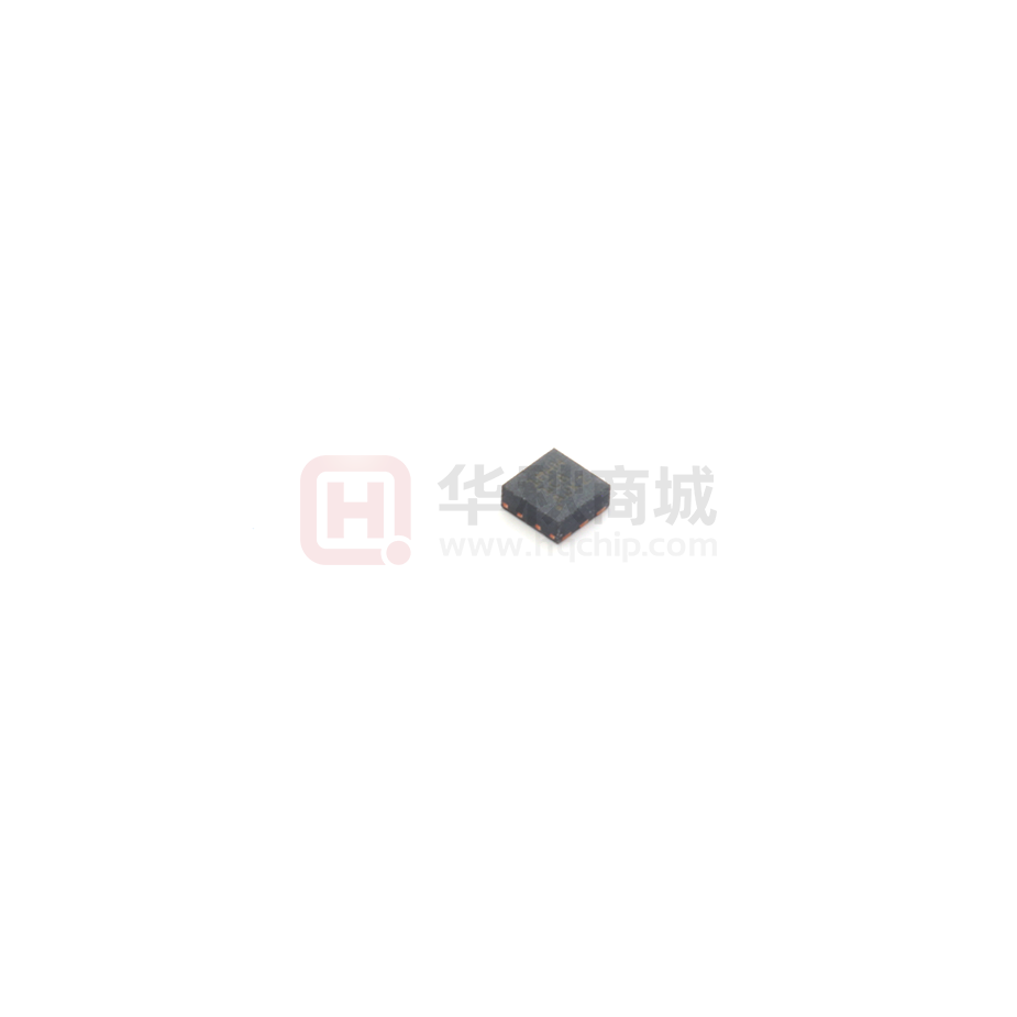
TLV758P 是一款可调 500A 低压降 (LDO) 稳压器。该
器件采用小型 6 引脚 2mm × 2mm WSON 封装和 5 引
脚 SOT23 封装并具有极低的静态电流,可提供快速的
线路和负载瞬态性能。TLV758P 特性 130mV 的超低
压降(500mA 电流情况下),这有助于提高系统的功
效。
输入电压范围:1.5V 至 6.0V
可调节输出电压:
– 0.55V 至 5.5V
低压降:
– 500mA 时为 130mV(最大值)(3.3 VOUT)
高输出精度:0.7%(典型值)和 1%(工作温度范
围内的最大值)
IQ:25µA(典型值)
内置软启动功能,具有单调 VOUT 上升
封装:
– 2mm × 2mm WSON-6 (DRV)
– SOT23-5 (DBV)(预览)
有源输出放电
TLV758P 针对各种 应用 进行了优化:支持 1.5V 至
6.0V 的输入电压范围以及 0.55V 至 5.5V 的外部可调
输出范围。这种低输出电压使得该 LDO 能够为具有较
低内核电压的现代微控制供电。
TLV758P 在与支持小尺寸总体解决方案的小型陶瓷输
出电容器搭配使用时,可保持稳定。一个精密带隙和误
差放大器具有高精度特性,在 25°C 时提供 0.7%(最
大值)的精度,在过温 (85ºC) 条件下提供 1%(最大
值)的精度。该器件包括集成的热关断、电流限制和欠
压锁定 (UVLO) 功能。TLV758P 包含一个内部折返电
流限制,有助于在短路事件中减少热耗散。
2 应用
•
•
•
•
•
•
•
机顶盒和游戏机
家庭影院和娱乐系统
台式机、笔记本电脑、超极本
打印机
服务器
恒温器和照明控制
电子销售终端 (EPOS)
器件信息(1)
器件型号
TLV758P
封装
封装尺寸(标称值)
WSON (6)
2.00mm × 2.00mm
SOT-23 (5)(2)
2.90mm × 1.60mm
(1) 如需了解所有可用封装,请参阅数据表末尾的可订购产品附
录。
(2) 预览器件。
典型应用
VIN
IN
CIN
VOUT
OUT
R1
TLV758P
GND
COUT
FB
R2
VEN
EN
DNC
1
本文档旨在为方便起见,提供有关 TI 产品中文版本的信息,以确认产品的概要。 有关适用的官方英文版本的最新信息,请访问 www.ti.com,其内容始终优先。 TI 不保证翻译的准确
性和有效性。 在实际设计之前,请务必参考最新版本的英文版本。
English Data Sheet: SBVS351
�TLV758P
ZHCSHZ4C – APRIL 2018 – REVISED MARCH 2019
www.ti.com.cn
目录
1
2
3
4
5
6
7
特性 ..........................................................................
应用 ..........................................................................
说明 ..........................................................................
修订历史记录 ...........................................................
Pin Configuration and Functions .........................
Specifications.........................................................
1
1
1
2
3
4
6.1
6.2
6.3
6.4
6.5
6.6
4
4
4
5
5
7
Absolute Maximum Ratings ......................................
ESD Ratings..............................................................
Recommended Operating Conditions.......................
Thermal Information ..................................................
Electrical Characteristics...........................................
Typical Characteristics ..............................................
Detailed Description ............................................ 13
7.1 Overview ................................................................. 13
7.2 Functional Block Diagram ....................................... 13
7.3 Feature Description................................................. 13
7.4 Device Functional Modes........................................ 15
8
Application and Implementation ........................ 16
8.1 Application Information............................................ 16
8.2 Typical Application .................................................. 20
9 Power Supply Recommendations...................... 22
10 Layout................................................................... 22
10.1 Layout Guidelines ................................................. 22
10.2 Layout Example .................................................... 22
11 器件和文档支持 ..................................................... 23
11.1
11.2
11.3
11.4
11.5
11.6
文档支持................................................................
接收文档更新通知 .................................................
社区资源................................................................
商标 .......................................................................
静电放电警告.........................................................
术语表 ...................................................................
23
23
23
23
23
23
12 机械、封装和可订购信息 ....................................... 23
4 修订历史记录
注:之前版本的页码可能与当前版本有所不同。
Changes from Revision B (March 2019) to Revision C
•
Deleted thermal pad from DBV pin out drawing .................................................................................................................... 3
Changes from Revision A (December 2018) to Revision B
•
Page
Page
已添加 DBV 封装,随 APL 发布 ............................................................................................................................................ 1
Changes from Original (April 2018) to Revision A
Page
•
已更改 将文档状态从“预告信息”更改成了“生产数据” ............................................................................................................. 1
2
Copyright © 2018–2019, Texas Instruments Incorporated
�TLV758P
www.ti.com.cn
ZHCSHZ4C – APRIL 2018 – REVISED MARCH 2019
5 Pin Configuration and Functions
DRV Package
6-Pin Adjustable WSON
Top View
OUT
1
6
FB
2
Thermal
5
pad
GND
3
4
DBV Package (Preview)
5-Pin Adjustable SOT-23
Top View
IN
DNC
IN
1
GND
2
EN
3
5
OUT
4
FB
EN
Not to scale
Not to scale
Pin Functions
PIN
NAME
I/O
DESCRIPTION
DRV
DBV
DNC
5
—
—
EN
4
3
Input
FB
2
4
—
This pin is used as an input to the control loop error amplifier and is used to
set the output voltage of the LDO.
GND
3
2
—
Ground pin
IN
OUT
Thermal pad
6
1
Enable pin. Drive EN greater than VEN(HI) to turn on the regulator.
Drive EN less than VEN(LO) to put the LDO into shutdown mode.
Input
Input pin. For best transient response and to minimize input impedance, use
the recommended value or larger ceramic capacitor from IN to ground as
listed in the Recommended Operating Conditions table and the Input and
Output Capacitor Selection section. Place the input capacitor as close to the
output of the device as possible.
Regulated output voltage pin. A capacitor is required from OUT to ground for
stability. For best transient response, use the nominal recommended value or
larger ceramic capacitor from OUT to ground; see the Recommended
Operating Conditions table and the Input and Output Capacitor Selection
section. Place the output capacitor as close to output of the device as
possible.
1
5
Output
Pad
—
—
Copyright © 2018–2019, Texas Instruments Incorporated
Do not connect
Connect the thermal pad to a large area GND plane for improved thermal
performance.
3
�TLV758P
ZHCSHZ4C – APRIL 2018 – REVISED MARCH 2019
www.ti.com.cn
6 Specifications
6.1 Absolute Maximum Ratings
over operating free-air temperature range (unless otherwise noted) (1)
Voltage
Temperature
(1)
(2)
MIN
MAX
Supply, VIN
–0.3
6.5
Enable, VEN
–0.3
6.5
Feedback, VFB
–0.3
2
Output, VOUT
–0.3
(2)
Operating junction, TJ
–40
150
Storage, Tstg
–65
150
VIN + 0.3
UNIT
V
°C
Stresses beyond those listed under Absolute Maximum Ratings may cause permanent damage to the device. Theseare stress ratings
only, which do not imply functional operation of the device at these or anyother conditions beyond those indicated under Recommended
OperatingConditions. Exposure to absolute-maximum-rated conditions for extended periods mayaffect device reliability.
The absolute maximum rating is VIN + 0.3V or 6.5 V, whichever is smaller.
6.2 ESD Ratings
VALUE
V(ESD)
(1)
(2)
Electrostatic discharge
Human-body model (HBM), per ANSI/ESDA/JEDEC JS-001 (1)
±2000
Charged-device model (CDM), per JEDEC specification JESD22-C101 (2)
±500
UNIT
V
JEDEC document JEP155 states that 500-V HBM allows safemanufacturing with a standard ESD control process. Manufacturing with
less than 500-V HBM ispossible with the necessary precautions.
JEDEC document JEP157 states that 250-V CDM allows safemanufacturing with a standard ESD control process. Manufacturing with
less than 250-V CDM ispossible with the necessary precautions.
6.3 Recommended Operating Conditions
over operating free-air temperature range (unless otherwise noted)
MIN
VIN
Input voltage
VOUT
NOM
MAX
UNIT
1.5
6.0
Output voltage
0.55
5.5
V
IOUT
Output current
0
500
mA
CIN
Input capacitor
1
COUT
Output capacitor (1)
1
220
VEN
Enable voltage (2)
0
6.0
V
fEN
Enable toggle frequency
10
kHz
TJ
Junction temperature
125
°C
(1)
(2)
4
–40
V
µF
µF
Minimum derated capacitance of 0.47 µF is required for stability
If VEN > VIN, when VEN > VUVLO rising (min), the input pin (IN) must sink 1 mA of current to avoid the device being turn on with floating
input pin.
Copyright © 2018–2019, Texas Instruments Incorporated
�TLV758P
www.ti.com.cn
ZHCSHZ4C – APRIL 2018 – REVISED MARCH 2019
6.4 Thermal Information
TLV758P
THERMAL METRIC
DBV (SOT-23)
DRV (WSON)
5 PINS
6 PINS
UNIT
RθJA
Junction-to-ambient thermal resistance
176.9
80.3
°C/W
RθJC(top)
Junction-to-case (top) thermal resistance
95.3
98.7
°C/W
RθJB
Junction-to-board thermal resistance
45.0
44.8
°C/W
ψJT
Junction-to-top characterization parameter
21.0
6.1
°C/W
ψJB
Junction-to-board characterization parameter
44.8
45.0
°C/W
RθJC(bot)
Junction-to-case (bottom) thermal resistance
N/A
20.8
°C/W
6.5 Electrical Characteristics
at operating temperature range (TJ = –40°C to +125°C),VIN = VOUT(NOM) + 0.5 V or 1.5 V (whichever isgreater), IOUT = 1 mA,
VEN =VIN, and CIN = COUT = 1 uF(unless otherwise noted); all typical values are at TJ = 25°C
PARAMETER
VFB
Feedback voltage
TEST CONDITIONS
–0.7%
–40°C ≤ TJ ≤ +85°C
–40°C ≤ TJ ≤ +125°C
Line regulation
VOUT(NOM) + 0.5 V (2) ≤ VIN ≤ 6.0 V
Load regulation
0.1 mA ≤ IOUT ≤ 500 mA, VIN ≥ 2.0 V
IGND
Ground current
IGND
Ground current
ISHDN
Shutdown current
IFB
Feedback pin current
ICL
Output current limit
ISC
Short-circuit current limit
VDO
Dropout voltage
IOUT = 0 mA
VIN = VOUT(NOM) + 1.0 V
IOUT = 500 mA,
–40°C ≤ TJ ≤ +125°C,
VOUT = 0.95 × VOUT(NOM)
MAX
V
–1%
1%
1.5%
2
TJ = 25°C
7.5
0.030
10
25
µA
35
µA
0.1
1
µA
0.01
0.1
µA
VOUT = VOUT(NOM) – 0.2 V,
VOUT < 1.5 V
530
720
865
VOUT = 0.9 V × VOUT(NOM),
VOUT ≥ 1.5 V
530
720
865
mA
VOUT = 0 V
350
0.65 V ≤ VOUT < 0.8 V
720
880
0.8 V ≤ VOUT < 1.0 V
585
750
1.0 V ≤ VOUT < 1.2 V
420
570
1.2 V ≤ VOUT < 1.5 V
285
400
1.5 V ≤ VOUT < 1.8 V
180
235
1.8 V ≤ VOUT < 2.5 V
140
185
2.5 V ≤ VOUT < 3.3 V
102
140
3.3 V ≤ VOUT ≤ 5.5 V
95
130
f = 1 kHz
50
f = 100 kHz
45
f = 1 MHz
30
Power-supply rejection ratio
VIN = VOUT(NOM) + 1.0 V,
IOUT = 50 mA
Vn
Output noise voltage
BW = 10 Hz to 100 kHz, VOUT = 0.9 V
mV
V/A
31
–40°C ≤ TJ ≤ +125°C
PSRR
UNIT
0.7%
–1.5%
VEN ≤ 0.3 V, 1.5 V ≤ VIN ≤ 6.0 V
VIN = VOUT(NOM) + 1.0 V
TYP
0.55
TJ = 25°C
Output accuracy (1)
MIN
TJ = 25°C
mA
mV
dB
53
µVRMS
VIN rising
1.21
1.33
1.47
V
VIN falling
1.17
1.29
1.42
V
VUVLO
Undervoltage lockout
VUVLO,
Undervoltage lockout hysteresis
VIN Hysteresis
tSTR
Startup time
From EN low-to-high transition to VOUT = VOUT(NOM) × 95%
VEN(HI)
EN pin high voltage
VEN(LO)
EN pin low voltage
IEN
Enable pin current
VIN = EN = 6.0 V
10
nA
RPULL
Pulldown resistance
VIN = 6.0 V
95
Ω
HYST
DOWN
(1)
(2)
40
mV
500
µs
1.0
V
0.3
V
When the device is connected to external feedback resistors at the FB pin, external resistor tolerances are not included
VIN = 1.5V for VOUT < 1.0 V
Copyright © 2018–2019, Texas Instruments Incorporated
5
�TLV758P
ZHCSHZ4C – APRIL 2018 – REVISED MARCH 2019
www.ti.com.cn
Electrical Characteristics (continued)
at operating temperature range (TJ = –40°C to +125°C),VIN = VOUT(NOM) + 0.5 V or 1.5 V (whichever isgreater), IOUT = 1 mA,
VEN =VIN, and CIN = COUT = 1 uF(unless otherwise noted); all typical values are at TJ = 25°C
PARAMETER
TSD
6
Thermal shutdown
TEST CONDITIONS
MIN
TYP
Shutdown, temperature increasing
170
Reset, temperature decreasing
155
MAX
UNIT
°C
版权 © 2018–2019, Texas Instruments Incorporated
�TLV758P
www.ti.com.cn
ZHCSHZ4C – APRIL 2018 – REVISED MARCH 2019
6.6 Typical Characteristics
0.6
0.6
0.45
0.45
Output Voltage Accuracy (%)
Output Voltage Accuracy (%)
at operating temperature range TJ = 25°C, VIN = VOUT(NOM) + 0.5 V or 1.5 V (whichever is greater), IOUT = 1 mA, VEN = VIN, and
CIN = COUT = 1 µF (unless otherwise noted)
0.3
0.15
0
-0.15
-0.3
-0.45
-0.6
3.8
±
±
4
4.2
qC
qC
4.4
4.6
TJ
± qC
0qC
4.8
5
25qC
85qC
5.2
5.4
125qC
150qC
5.6
5.8
0.3
0.15
0
-0.15
-0.3
-0.45
-0.6
1.5
6
±
±
2
Input Voltage (V)
VOUT = 3.3 V, IOUT = 1 mA
图 1. 3.3-V Line Regulation vs VIN
3
3.5
4
4.5
125qC
150qC
5
5.5
6
0.45
0.5
0.45
0.5
图 2. 0.55-V Line Regulation vs VIN
160
140
0.2
Dropout Voltage (mV)
Output Voltage Accuracy (%)
2.5
25qC
85qC
Input Voltage (V)
VOUT = 0.55 V, IOUT = 1 mA
0.3
0.1
0
-0.1
TJ
± qC
0qC
-0.2
±
±
qC
qC
25qC
85qC
±
±
qC
qC
0.05
0.1
TJ
± qC
0qC
25qC
85qC
125qC
150qC
120
100
80
60
40
20
125qC
150qC
0
-0.3
5.5
5.6
5.7
5.8
5.9
0
6
图 3. 5.5-V Line Regulation vs VIN
870
140
Dropout Voltage (mV)
160
840
810
780
750
720
690
±
±
qC
qC
0.2
0.25
0.3
0.35
0.4
图 4. 3.3-V Dropout Voltage vs IOUT
900
TJ
± qC
0qC
0.15
Output Current (A)
Input Voltage (V)
VOUT = 5.5 V, IOUT = 1 mA
Dropout Voltage (mV)
TJ
± qC
0qC
qC
qC
25qC
85qC
125qC
150qC
660
±
±
qC
qC
0.05
0.1
TJ
± qC
0qC
25qC
85qC
125qC
150qC
120
100
80
60
40
20
0
0
0.05
0.1
0.15
0.2
0.25
0.3
0.35
0.4
Output Current (A)
图 5. 0.55-V Dropout Voltage vs IOUT
版权 © 2018–2019, Texas Instruments Incorporated
0.45
0.5
0
0.15
0.2
0.25
0.3
0.35
0.4
Output Current (A)
图 6. 5.5-V Dropout Voltage vs IOUT
7
�TLV758P
ZHCSHZ4C – APRIL 2018 – REVISED MARCH 2019
www.ti.com.cn
Typical Characteristics (接
接下页)
at operating temperature range TJ = 25°C, VIN = VOUT(NOM) + 0.5 V or 1.5 V (whichever is greater), IOUT = 1 mA, VEN = VIN, and
CIN = COUT = 1 µF (unless otherwise noted)
1,000
800
±
±
800
TJ
± qC
0qC
qC
qC
25qC
85qC
125qC
150qC
700
Ground Pin Current (PA)
Dropout Voltage (mV)
900
700
600
500
400
300
200
600
500
400
300
200
100
100
0
0.5
±
±
1.5
2
2.5
3
3.5
4
4.5
5
0
0.05
0.1
0.15
图 7. VDO vs VOUT
0.2
0.25
0.3
0.35
0.4
0.45
0.5
图 8. IGND vs IOUT
560
TJ
± qC
0qC
qC
qC
25qC
85qC
125qC
150qC
±
±
480
Ground Pin Current (PA)
±
±
1,800
Shutdown Current (nA)
125qC
150qC
Output Current (A)
2,100
1,500
1,200
900
600
300
0
TJ
± qC
0qC
qC
qC
25qC
85qC
125qC
150qC
400
320
240
160
80
0
-300
-80
0
0.6
1.2
1.8
2.4
3
3.6
4.2
4.8
5.4
6
0
0.6
Input Voltage (V)
VEN = 0 V
1.2
1.8
2.4
3
3.6
4.2
4.8
5.4
6
Input Voltage (V)
VOUT = 3.3 V, IOUT = 0 mA
图 9. ISHDN vs VIN
图 10. IQ vs VIN
1
0.6
±
±
0.75
TJ
± qC
0qC
qC
qC
25qC
85qC
125qC
150qC
0.5
0.25
0
-0.25
-0.5
-0.75
±
±
0.45
Change in VOUT (%)
Change in VOUT (%)
25qC
85qC
0
1
Output Voltage (V)
IOUT = 500 mA
TJ
± qC
0qC
qC
qC
25qC
85qC
125qC
150qC
0.3
0.15
0
-0.15
-0.3
-0.45
-1
-0.6
0
0.05
0.1
VIN
0.15
0.2
0.25
0.3
0.35
0.4
Output Current (A)
= 3.8 V, VOUT = 3.3 V
图 11. 3.3-V Load Regulation vs IOUT
8
TJ
± qC
0qC
qC
qC
0.45
0.5
0
0.05
0.1
0.15
VIN
0.2
0.25
0.3
0.35
0.4
0.45
0.5
Output Current (A)
= 2 V, VOUT = 0.55 V
图 12. 0.55-V Load Regulation vs IOUT
版权 © 2018–2019, Texas Instruments Incorporated
�TLV758P
www.ti.com.cn
ZHCSHZ4C – APRIL 2018 – REVISED MARCH 2019
Typical Characteristics (接
接下页)
at operating temperature range TJ = 25°C, VIN = VOUT(NOM) + 0.5 V or 1.5 V (whichever is greater), IOUT = 1 mA, VEN = VIN, and
CIN = COUT = 1 µF (unless otherwise noted)
640
1
±
±
qC
qC
25qC
85qC
125qC
150qC
±
±
560
0.5
Output Voltage (mV)
0.25
0
-0.25
-0.5
125qC
150qC
400
320
240
160
80
0
-1
0
0.05
0.1
0.15
VIN
0.2
0.25
0.3
0.35
0.4
0.45
0
0.5
0.5
1
1.5
2
2.5
3
3.5
4
4.5
5
Pulldown Current (mA)
Output Current (A)
= 6 V, VOUT = 5.5 V
图 13. 5-V Load Regulation vs IOUT
图 14. VOUT vs IOUT Pulldown Resistor
840
300
VEN(LO)
800
VEN(HI)
±
±
250
760
Enable Pin Current (PA)
Enable Threshold (mV)
25qC
85qC
480
-0.75
720
680
640
600
560
520
TJ
± qC
0qC
qC
qC
125qC
85qC
125qC
150qC
200
150
100
50
0
480
440
-50
-50
-25
0
25
50
75
100
125
150
0
0.5
1
Temperature (qC)
图 15. VEN(HI) and VEN(LO) vs Temperature
4.5
TJ
-20qC
0qC
-50qC
-40qC
4
25qC
85qC
125qC
Input Voltage (V)
3
2.5
2
1.5
1
0.5
0
100
200
300
400
2
2.5
3
3.5
4
4.5
5
5.5
图 16. IEN vs VIN
3.5
0
1.5
Input Voltage (V)
VEN = 5.5 V
5
Output Voltage (V)
TJ
± qC
0qC
qC
qC
500
600
Output Current (mA)
700
14
13
12
11
10
9
8
7
6
5
4
3
2
1
0
0
0.5
1
Time (ms)
1.5
25
Vin
20
Vout 15
10
5
0
-5
-10
-15
-20
-25
-30
-35
-40
-45
2
AC-coupled Output Voltage (mV)
Change in VOUT (%)
0.75
TJ
± qC
0qC
VOUT = 0.55 V, IOUT = 1 mA, VIN slew rate = 1 V/µs
图 17. 3.3-V Foldback Current Limit vs IOUT
版权 © 2018–2019, Texas Instruments Incorporated
图 18. 0.55-V Line Transient
9
�TLV758P
ZHCSHZ4C – APRIL 2018 – REVISED MARCH 2019
www.ti.com.cn
Typical Characteristics (接
接下页)
0.2
0.4
0.6
0.8
1
1.2
Time (ms)
1.4
1.6
4
200
Iout
Vout 150
100
3.5
3
2.5
50
2
0
1.5
-50
1
-100
0.5
-150
0
-200
-0.5
-250
-1
0
50
Iout
Vout 150
100
3.5
Output Current (A)
3
2.5
50
2
0
1.5
-50
1
-100
0.5
-150
0
-200
-0.5
-1
150
200 250 300
Time (us)
350
350
400
450
400
450
4
AC-coupled Output Voltage (mV)
Output Current (A)
200
100
200 250 300
Time (us)
-300
500
图 20. 3.3-V, 1-mA to 500-mA Load Transient
图 19. 3.3-V Line Transient
4
50
150
VIN = 3.8 V, VOUT = 3.3 V, IOUT slew rate = 1 A/µs
VOUT = 3.3 V, IOUT = 1 mA, VIN slew rate = 1 V/µs
0
100
200
Iout
Vout 150
100
3.5
3
2.5
50
2
0
1.5
-50
1
-100
0.5
-150
0
-200
-250
-0.5
-250
-300
500
-1
0
50
VIN = 2 V, VOUT = 0.55 V, IOUT slew rate = 1 A/µs
100
150
200 250 300
Time (us)
350
400
450
AC-coupled Output Voltage (mV)
0
120
Vin
100
Vout 80
60
40
20
0
-20
-40
-60
-80
-100
-120
-140
-160
1.8
2
AC-coupled Output Voltage (mV)
10
9.5
9
8.5
8
7.5
7
6.5
6
5.5
5
4.5
4
3.5
3
AC-coupled Output Voltage (mV)
Output Current (A)
Input Voltage (V)
at operating temperature range TJ = 25°C, VIN = VOUT(NOM) + 0.5 V or 1.5 V (whichever is greater), IOUT = 1 mA, VEN = VIN, and
CIN = COUT = 1 µF (unless otherwise noted)
-300
500
VIN = 5.5 V, VOUT = 5 V, IOUT slew rate = 1 A/µs
图 21. 0.55-V, 1-mA to 500-mA Load Transient
图 22. 5-V, 1-mA to 500-mA Load Transient
5
5
4.5
4
4
3.5
3
Voltage (V)
Voltage (V)
3
2.5
2
1.5
1
2
1
0.5
0
Vout
Vin
-0.5
-1
-1
0
200
400
600
Time (us)
800
VIN = 3.8 V, VOUT = 3.3 V, IOUT = 1 mA
图 23. VIN Power-Up
10
Vout
Venable
Vin
0
1,000
0
200
400
600
Time (us)
800
1,000
VIN = 3.8 V, VOUT = 3.3 V, IOUT = 1 mA
图 24. Startup With EN
版权 © 2018–2019, Texas Instruments Incorporated
�TLV758P
www.ti.com.cn
ZHCSHZ4C – APRIL 2018 – REVISED MARCH 2019
Typical Characteristics (接
接下页)
at operating temperature range TJ = 25°C, VIN = VOUT(NOM) + 0.5 V or 1.5 V (whichever is greater), IOUT = 1 mA, VEN = VIN, and
CIN = COUT = 1 µF (unless otherwise noted)
90
VIN = 3.5 V
VIN = 3.6 V
VIN = 3.7 V
VIN = 3.8 V
80
70
60
50
40
30
20
10
0
10
100
1k
10k
100k
Frequency (Hz)
1M
Power-Supply Rejection Ratio (dB)
Power-Supply Rejection Ratio (dB)
90
80
70
60
50
40
30
20
10
0
10
10M
VOUT = 3.3 V, IOUT = 500 mA, COUT = 2.2 µF
图 25. PSRR vs Frequency and VIN
VIN = 3.5 V
VIN = 3.6 V
VIN = 3.7 V
VIN = 3.8 V
70
60
50
40
30
20
10
100
1k
10k
100k
Frequency (Hz)
1M
Power-Supply Rejection Ratio (dB)
Power-Supply Rejection Ratio (dB)
10k
100k
Frequency (Hz)
1M
10M
图 26. PSRR vs Frequency and VIN
80
70
60
50
40
30
20
10
0
10
10M
VOUT = 3.3 V, IOUT = 250 mA, COUT = 2.2 µF
VIN = 3.9 V
VIN = 4.0 V
VIN = 4.1 V
VIN = 4.2 V
VIN = 4.3 V
100
1k
10k
100k
Frequency (Hz)
1M
10M
VOUT = 3.3 V, IOUT = 250 mA, COUT = 2.2 µF
图 27. PSRR vs Frequency and VIN
图 28. PSRR vs Frequency and VIN
90
VIN = 1.9 V, VOUT = 0.9 V
VIN = 2.8 V, VOUT = 1.8 V
VIN = 4.3 V, VOUT = 3.3 V
80
70
60
50
40
30
20
10
100
1k
10k
100k
Frequency (Hz)
IOUT = 500 mA, COUT = 2.2 µF
图 29. PSRR vs Frequency
版权 © 2018–2019, Texas Instruments Incorporated
1M
10M
Power-Supply Rejection Ratio (dB)
90
Power-Supply Rejection Ratio (dB)
1k
90
80
0
10
100
VOUT = 3.3 V, IOUT = 500 mA, COUT = 2.2 µF
90
0
10
VIN = 3.9 V
VIN = 4.0 V
VIN = 4.1 V
VIN = 4.2 V
VIN = 4.3 V
COUT = 1 PF
COUT = 2.2 PF
COUT = 4.7 PF
COUT = 47 PF
80
70
60
50
40
30
20
10
0
10
100
1k
10k
100k
Frequency (Hz)
1M
10M
VIN = 3.8 V, VOUT = 3.3 V, IOUT = 500 mA
图 30. PSRR vs Frequency and COUT
11
�TLV758P
ZHCSHZ4C – APRIL 2018 – REVISED MARCH 2019
www.ti.com.cn
Typical Characteristics (接
接下页)
at operating temperature range TJ = 25°C, VIN = VOUT(NOM) + 0.5 V or 1.5 V (whichever is greater), IOUT = 1 mA, VEN = VIN, and
CIN = COUT = 1 µF (unless otherwise noted)
90
CFF = 0 nF
CFF = 1 nF
CFF = 10 nF
CFF = 100 nF
80
70
Power-Supply Rejection Ratio (dB)
Power-Supply Rejection Ratio (dB)
90
60
50
40
30
20
10
0
10
100
1k
10k
100k
Frequency (Hz)
1M
80
70
60
50
40
30
ILOAD = 10 mA
ILOAD = 100 mA
ILOAD = 250 mA
ILOAD = 500 mA
20
10
0
10
10M
VIN = 3.8 V, VOUT = 3.3 V, IOUT = 500 mA
图 31. PSRR vs Frequency and CFF
1M
10M
图 32. PSRR vs Frequency and ILOAD
IOUT= 10mA, 159PVRMS
IOUT= 100mA, 160PVRMS
IOUT= 500mA, 160PVRMS
5
CFF = 0 nF, 160 PVRMS
CFF = 1 nF, 108 PVRMS
CFF = 10 nF, 74 PVRMS
CFF = 100 nF, 44 PVRMS
10
5
2
Noise (PV/—Hz)
2
Noise (PV/—Hz)
10k
100k
Frequency (Hz)
20
10
1
0.5
0.2
0.1
1
0.5
0.2
0.1
0.05
0.05
0.02
0.02
0.01
0.01
0.005
10
0.005
10
100
1k
10k
100k
Frequency (Hz)
1M
10M
VIN = 3.8 V, VOUT = 3.3 V, COUT = 2.2 µF,
VRMS BW = 10 Hz to 100 kHz
100
1k
10k
100k
Frequency (Hz)
1M
10M
VIN = 3.8 V, VOUT = 3.3 V, IOUT = 500 mA, COUT = 2.2 µF,
VRMS BW = 10 Hz to 100 kHz
图 33. Output Spectral Noise Density
图 34. Output Spectral Noise Density vs
Frequency and CFF
20
20
COUT = 2.2PF, 160 PVRMS
COUT = 4.7PF, 170 PVRMS
COUT = 47PF, 138 PVRMS
10
5
VIN=1.9V, VOUT=0.9V, 53PVRMS
VIN=2.8V, VOUT=1.8V, 96PVRMS
VIN=3.8V, VOUT=3.3V, 160PVRMS
10
5
2
Noise (PV/—Hz)
2
Noise (PV/—Hz)
1k
VIN = 3.8 V, VOUT = 3.3 V, COUT = 2.2 µF
20
1
0.5
0.2
0.1
1
0.5
0.2
0.1
0.05
0.05
0.02
0.02
0.01
0.01
0.005
10
0.005
10
100
1k
10k
100k
Frequency (Hz)
1M
VIN = 3.8 V, VOUT = 3.3 V, IOUT = 100 mA, CFF = 0 µF,
VRMS BW = 10 Hz to 100 kHz
图 35. Output Spectral Noise Density vs
Frequency and COUT
12
100
10M
100
1k
10k
100k
Frequency (Hz)
1M
10M
IOUT = 500 mA, COUT = 2.2 µF, VRMS BW = 10 Hz to 100 kHz
图 36. Output Spectral Noise Density vs Frequency
版权 © 2018–2019, Texas Instruments Incorporated
�TLV758P
www.ti.com.cn
ZHCSHZ4C – APRIL 2018 – REVISED MARCH 2019
7 Detailed Description
7.1 Overview
The TLV758P low-dropout regulators (LDO) consumes low quiescent current and delivers excellent line and load
transient performance. These characteristics, combined with low noise and good PSRR with low dropout voltage,
make this device ideal for portable consumer applications.
This regulator offers foldback current limit, shutdown, and thermal protection. The operating junction temperature
for this device is –40°C to +125°C.
7.2 Functional Block Diagram
OUT
IN
Current
Limit
–
+
Thermal
Shutdown
FB
UVLO
EN
95 �
Band Gap
GND
Logic
7.3 Feature Description
7.3.1 Undervoltage Lockout (UVLO)
The TLV758P uses an undervoltage lockout (UVLO) circuit that disables the output until the input voltage is
greater than the rising UVLO voltage (VUVLO). This circuit ensures that the device does not exhibit any
unpredictable behavior when the supply voltage is lower than the operational range of the internal circuitry. When
VIN is less than VUVLO, the output is connected to ground with a pulldown resistor (RPULLDOWN).
7.3.2 Shutdown
The enable pin (EN) is active high. Enable the device by forcing the EN pin to exceed VEN(HI). Turn off the device
by forcing the EN pin to drop below VEN(LO). If shutdown capability is not required, connect EN to IN.
The TLV758P has an internal pulldown MOSFET that connects an RPULLDOWN resistor to ground when the device
is disabled. The discharge time after disabling depends on the output capacitance (COUT) and the load resistance
(RL) in parallel with the pulldown resistor (RPULLDOWN). 公式 1 calculates the time constant:
τ = ( RPULLDOWN × RL) / (RPULLDOWN + RL)
Copyright © 2018–2019, Texas Instruments Incorporated
(1)
13
�TLV758P
ZHCSHZ4C – APRIL 2018 – REVISED MARCH 2019
www.ti.com.cn
Feature Description (continued)
7.3.3 Foldback Current Limit
The device has an internal current limit circuit that protects the regulator during transient high-load current faults
or shorting events. The current limit is a hybrid brickwall-foldback scheme. The current limit transitions from a
brickwall scheme to a foldback scheme at the foldback voltage (VFOLDBACK). In a high-load current fault with the
output voltage above VFOLDBACK, the brickwall scheme limits the output current to the current limit (ICL). When the
voltage drops below VFOLDBACK, a foldback current limit activates that scales back the current as the output
voltage approaches GND. When the output is shorted, the device supplies a typical current called the shortcircuit current limit (ISC). ICL and ISC are listed in the Electrical Characteristics table.
For this device, VFOLDBACK = 0.4 V × VOUT(NOM).
The output voltage is not regulated when the device is in current limit. When a current limit event occurs, the
device begins to heat up because of the increase in power dissipation. When the device is in brickwall current
limit, the pass transistor dissipates power [(VIN – VOUT) × ICL]. When the device output is shorted and the output
is below VFOLDBACK, the pass transistor dissipates power [(VIN – VOUT) × ISC]. If thermal shutdown is triggered, the
device turns off. After the device cools down, the internal thermal shutdown circuit turns the device back on. If
the output current fault condition continues, the device cycles between current limit and thermal shutdown. For
more information on current limits, see the Know Your Limits application report.
Figure 37 shows a diagram of the foldback current limit.
VOUT
Brickwall
VOUT(NOM)
VFOLDBACK
Foldback
IOUT
0V
0 mA
ISC
IRATED
ICL
Figure 37. Foldback Current Limit
7.3.4 Thermal Shutdown
Thermal shutdown protection disables the output when the junction temperature rises to approximately 170°C.
Disabling the device eliminates the power dissipated by the device, allowing the device to cool. When the
junction temperature cools to approximately 155°C, the output circuitry is again enabled. Depending on power
dissipation, thermal resistance, and ambient temperature, the thermal protection circuit may cycle on and off.
This cycling limits regulator dissipation, protecting the LDO from damage as a result of overheating.
Activating the thermal shutdown feature usually indicates excessive power dissipation as a result of the product
of the (VIN – VOUT) voltage and the load current. For reliable operation, limit junction temperature to 125°C
maximum. To estimate the margin of safety in a complete design, increase the ambient temperature until the
thermal protection is triggered; use worst-case loads and signal conditions.
14
Copyright © 2018–2019, Texas Instruments Incorporated
�TLV758P
www.ti.com.cn
ZHCSHZ4C – APRIL 2018 – REVISED MARCH 2019
Feature Description (continued)
The TLV758P internal protection circuitry protects against overload conditions but is not intended to be activated
in normal operation. Continuously running the TLV758P into thermal shutdown degrades device reliability.
7.4 Device Functional Modes
7.4.1 Device Functional Mode Comparison
The Device Functional Mode Comparison table shows the conditions that lead to the different modes of
operation. See the Electrical Characteristics table for parameter values.
Table 1. Device Functional Mode Comparison
PARAMETER
OPERATING MODE
VIN
VEN
IOUT
TJ
Normal operation
VIN > VOUT(nom) + VDO and VIN > VIN(min)
VEN > VEN(HI)
IOUT < IOUT(max)
TJ < TSD(shutdown)
Dropout operation
VIN(min) < VIN < VOUT(nom) + VDO
VEN > VEN(HI)
IOUT < IOUT(max)
TJ < TSD(shutdown)
VIN < VUVLO
VEN < VEN(LOW)
Not applicable
TJ > TSD(shutdown)
Disabled
(any true condition
disables the device)
7.4.2 Normal Operation
The device regulates to the nominal output voltage when the following conditions are met:
• The input voltage is greater than the nominal output voltage plus the dropout voltage (VOUT(nom) + VDO)
• The output current is less than the current limit (IOUT < ICL)
• The device junction temperature is less than the thermal shutdown temperature (TJ < TSD)
• The enable voltage has previously exceeded the enable rising threshold voltage and has not yet decreased to
less than the enable falling threshold
7.4.3 Dropout Operation
If the input voltage is lower than the nominal output voltage plus the specified dropout voltage, but all other
conditions are met for normal operation, the device operates in dropout mode. In this mode, the output voltage
tracks the input voltage. During this mode, the transient performance of the device becomes significantly
degraded because the pass transistor is in the ohmic or triode region, and acts as a switch. Line or load
transients in dropout can result in large output-voltage deviations.
When the device is in a steady dropout state (defined as when the device is in dropout, VIN < VOUT(NOM) + VDO,
directly after being in a normal regulation state, but not during startup), the pass transistor is driven into the
ohmic or triode region. When the input voltage returns to a value greater than or equal to the nominal output
voltage plus the dropout voltage (VOUT(NOM) + VDO), the output voltage can overshoot for a short period of time
while the device pulls the pass transistor back into the linear region.
7.4.4 Disabled
The output of the device can be shutdown by forcing the voltage of the enable pin to less than the maximum EN
pin low-level input voltage (see the Electrical Characteristics table). When disabled, the pass transistor is turned
off, internal circuits are shutdown, and the output voltage is actively discharged to ground by an internal
discharge circuit from the output to ground.
版权 © 2018–2019, Texas Instruments Incorporated
15
�TLV758P
ZHCSHZ4C – APRIL 2018 – REVISED MARCH 2019
www.ti.com.cn
8 Application and Implementation
注
Information in the following applications sections is not part of the TI component
specification, and TI does not warrant its accuracy or completeness. TI’s customers are
responsible for determining suitability of components for their purposes. Customers should
validate and test their design implementation to confirm system functionality.
8.1 Application Information
8.1.1 Adjustable Device Feedback Resistors
图 38 shows that the output voltage of the TLV758P can be adjusted from 0.55 V to 5.5 V by using a resistor
divider network.
VIN
IN
CIN
VOUT
OUT
R1
TLV758P
GND
COUT
FB
R2
VEN
EN
DNC
图 38. Adjustable Operation
The adjustable-version device requires external feedback divider resistors to set the output voltage. VOUT is set
using the feedback divider resistors, R1 and R2, according to the following equation:
VOUT = VFB × (1 + R1 / R2)
(2)
For this device, VFB = 0.55 V.
To ignore the FB pin current error term in the VOUT equation, set the feedback divider current to 100x the FB pin
current listed in the Electrical Characteristics table. This setting provides the maximum feedback divider series
resistance, as shown in the following equation:
R1 + R2 ≤ VOUT / (IFB × 100)
(3)
For this device, IFB = 10 nA.
8.1.2 Input and Output Capacitor Selection
The TLV758P requires an output capacitance of 0.47 µF or larger for stability. Use X5R- and X7R-type ceramic
capacitors because these capacitors have minimal variation in value and equivalent series resistance (ESR) over
temperature. When choosing a capacitor for a specific application, pay attention to the dc bias characteristics for
the capacitor. Higher output voltages cause a significant derating of the capacitor. For best performance, the
maximum recommended output capacitance is 220 µF.
Although an input capacitor is not required for stability, good analog design practice is to connect a capacitor
from IN to GND. Some input supplies have a high impedance, thus placing the input capacitor on the input
supply helps reduce the input impedance. This capacitor counteracts reactive input sources and improves
transient response, input ripple, and PSRR. If the input supply has a high impedance over a large range of
frequencies, several input capacitors can be used in parallel to lower the impedance over frequency. Use a
higher-value capacitor if large, fast, rise-time load transients are anticipated, or if the device is located several
inches from the input power source.
16
版权 © 2018–2019, Texas Instruments Incorporated
�TLV758P
www.ti.com.cn
ZHCSHZ4C – APRIL 2018 – REVISED MARCH 2019
Application Information (接
接下页)
8.1.3 Dropout Voltage
The TLV758P uses a PMOS pass transistor to achieve low dropout. When (VIN – VOUT) is less than the dropout
voltage (VDO), the PMOS pass device is in the linear region of operation and the input-to-output resistance is the
RDS(ON) of the PMOS pass element. VDO scales approximately with output current because the PMOS device
behaves like a resistor in dropout mode. As with any linear regulator, PSRR and transient response degrade as
(VIN – VOUT) approaches dropout operation.
8.1.4 Exiting Dropout
Some applications have transients that place the LDO into dropout, such as slower ramps on VIN during start-up.
As with other LDOs, the output may overshoot on recovery from these conditions. A ramping input supply causes
an LDO to overshoot on start-up, as shown in 图 39, when the slew rate and voltage levels are in the correct
range. Use an enable signal to avoid this condition.
Input Voltage
Response time for
LDO to get back into
regulation.
Load current discharges
output voltage.
VIN = VOUT(nom) + VDO
Voltage
Output Voltage
Dropout
VOUT = VIN - VDO
Output Voltage in
normal regulation.
Time
图 39. Startup Into Dropout
Line transients out of dropout can also cause overshoot on the output of the regulator. These overshoots are
caused by the error amplifier having to drive the gate capacitance of the pass element and bring the gate back to
the correct voltage for proper regulation. 图 40 illustrates what is happening internally with the gate voltage and
how overshoot can be caused during operation. When the LDO is placed in dropout, the gate voltage (VGS) is
pulled all the way down to ground to give the pass device the lowest on-resistance as possible. However, if a line
transient occurs when the device is in dropout, the loop is not in regulation and can cause the output to
overshoot until the loop responds and the output current pulls the output voltage back down into regulation. If
these transients are not acceptable, then continue to add input capacitance in the system until the transient is
slow enough to reduce the overshoot.
版权 © 2018–2019, Texas Instruments Incorporated
17
�TLV758P
ZHCSHZ4C – APRIL 2018 – REVISED MARCH 2019
www.ti.com.cn
Application Information (接
接下页)
Transient response
time of the LDO
Input Voltage
Load current
discharges
output
voltage
VDO
Voltage
Output Voltage
Output Voltage in
normal regulation
Dropout
VOUT = VIN - VDO
VGS voltage
(pass device
fully off)
Input Voltage
VGS voltage for
normal operation
VGS voltage for
normal operation
Gate Voltage
VGS voltage in
dropout (pass device
fully on)
Time
图 40. Line Transients From Dropout
8.1.5 Reverse Current
As with most LDOs, excessive reverse current can damage this device.
Reverse current flows through the body diode on the pass element instead of the normal conducting channel. At
high magnitudes, this current flow degrades the long-term reliability of the device, as a result of one of the
following conditions:
• Degradation caused by electromigration
• Excessive heat dissipation
• Potential for a latch-up condition
Conditions where reverse current can occur are outlined in this section, all of which can exceed the absolute
maximum rating of VOUT > VIN + 0.3 V:
• If the device has a large COUT and the input supply collapses with little or no load current
• The output is biased when the input supply is not established
• The output is biased above the input supply
18
版权 © 2018–2019, Texas Instruments Incorporated
�TLV758P
www.ti.com.cn
ZHCSHZ4C – APRIL 2018 – REVISED MARCH 2019
Application Information (接
接下页)
If reverse current flow is expected in the application, external protection must be used to protect the device. 图
41 shows one approach of protecting the device.
Schottky Diode
IN
CIN
Internal Body Diode
Device
OUT
COUT
GND
图 41. Example Circuit for Reverse Current Protection Using a Schottky Diode
8.1.6 Power Dissipation (PD)
Circuit reliability requires consideration of the device power dissipation, location of the circuit on the printed circuit
board (PCB), and correct sizing of the thermal plane. The PCB area around the regulator must have few or no
other heat-generating devices that cause added thermal stress.
To first-order approximation, power dissipation in the regulator depends on the input-to-output voltage difference
and load conditions. Equation 4 calculates power dissipation (PD).
PD = (VIN – VOUT) × IOUT
(4)
NOTE
Power dissipation can be minimized, and therefore greater efficiency can be achieved, by
correct selection of the system voltage rails. For the lowest power dissipation use the
minimum input voltage required for correct output regulation.
For devices with a thermal pad, the primary heat conduction path for the device package is through the thermal
pad to the PCB. Solder the thermal pad to a copper pad area under the device. This pad area must contain an
array of plated vias that conduct heat to additional copper planes for increased heat dissipation.
The maximum power dissipation determines the maximum allowable ambient temperature (TA) for the device.
According to Equation 5, power dissipation and junction temperature are most often related by the junction-toambient thermal resistance (RθJA) of the combined PCB and device package and the temperature of the ambient
air (TA).
TJ = TA + (RθJA × PD)
(5)
Thermal resistance (RθJA) is highly dependent on the heat-spreading capability built into the particular PCB
design, and therefore varies according to the total copper area, copper weight, and location of the planes. The
junction-to-ambient thermal resistance listed in the Thermal Information table is determined by the JEDEC
standard PCB and copper-spreading area, and is used as a relative measure of package thermal performance.
8.1.7 Feed-Forward Capacitor (CFF)
For the adjustable-voltage version device, a feed-forward capacitor (CFF) can be connected from the OUT pin to
the FB pin. CFF improves transient, noise, and PSRR performance, but is not required for regulator stability.
Recommended CFF values are listed in the Recommended Operating Conditions table. A higher capacitance CFF
can be used; however, the startup time increases. For a detailed description of CFF tradeoffs, see the Pros and
Cons of Using a Feedforward Capacitor with a Low-Dropout Regulator application report.
版权 © 2018–2019, Texas Instruments Incorporated
19
�TLV758P
ZHCSHZ4C – APRIL 2018 – REVISED MARCH 2019
www.ti.com.cn
8.2 Typical Application
图 42 shows the typical application circuit for the TLV758P. Input and output capacitances must be at least 1 µF.
VIN
IN
CIN
VOUT
OUT
R1
TLV758P
GND
COUT
FB
R2
VEN
EN
DNC
图 42. TLV758P Typical Application
8.2.1 Design Requirements
Use the parameters listed in 表 2 for typical linear regulator applications.
表 2. Design Parameters
PARAMETER
DESIGN REQUIREMENT
Input voltage
3.8 V
Output voltage
3.3 V, ±1%
Input current
500 mA (maximum)
Output load
500-mA DC
Maximum ambient temperature
70°C
8.2.2 Detailed Design Procedure
Input and output capacitors are required to achieve the output voltage transient requirements. Capacitance
values of 2.2 µF are selected to give the maximum output capacitance in a small, low-cost package; see the
Input and Output Capacitor Selection section for details.
图 38 illustrates the output voltage of the TLV758P; set the output voltage using the resistor divider.
8.2.2.1 Input Current
During normal operation, the input current to the LDO is approximately equal to the output current of the LDO.
During startup, the input current is higher as a result of the inrush current charging the output capacitor. Use 公式
6 to calculate the current through the input.
VOUT(t)
COUT ´ dVOUT(t)
IOUT(t) =
+
RLOAD
dt
where:
•
•
•
20
VOUT(t) is the instantaneous output voltage of the turn-on ramp
dVOUT(t) / dt is the slope of the VOUT ramp
RLOAD is the resistive load impedance
(6)
版权 © 2018–2019, Texas Instruments Incorporated
�TLV758P
www.ti.com.cn
ZHCSHZ4C – APRIL 2018 – REVISED MARCH 2019
8.2.2.2 Thermal Dissipation
The junction temperature can be determined using the junction-to-ambient thermal resistance (RθJA) and the total
power dissipation (PD). Use 公式 7 to calculate the power dissipation. Multiply PD by RθJA as 公式 8 shows and
add the ambient temperature (TA) to calculate the junction temperature (TJ).
PD = (IGND+ IOUT) × (VIN – VOUT)
TJ = RθJA × PD + TA
(7)
(8)
Calculate the maximum ambient temperature as 公式 9 shows if the (TJ(MAX)) value does not exceed 125°C. 公式
10 calculates the maximum ambient temperature with a value of 104.93°C.
TA(MAX) = TJ(MAX) – RθJA × PD
TA(MAX) = 125°C – 80.3°C/W × (3.8 V – 3.3 V) × (0.5 A) = 104.93°C
(9)
(10)
8.2.3 Application Curve
Power-Supply Rejection Ratio (dB)
90
80
70
60
50
40
30
ILOAD = 10 mA
ILOAD = 100 mA
ILOAD = 250 mA
ILOAD = 500 mA
20
10
0
10
100
1k
10k
100k
Frequency (Hz)
1M
10M
VIN = 3.8 V, VOUT = 3.3 V, COUT = 2.2 µF
图 43. PSRR vs Frequency and ILOAD
版权 © 2018–2019, Texas Instruments Incorporated
21
�TLV758P
ZHCSHZ4C – APRIL 2018 – REVISED MARCH 2019
www.ti.com.cn
9 Power Supply Recommendations
Connect a low output impedance power supply directly to the IN pin of the TLV758P.
10 Layout
10.1 Layout Guidelines
•
•
•
•
Place input and output capacitors as close to the device as possible.
Use copper planes for device connections, in order to optimize thermal performance.
Place thermal vias around the device to distribute the heat.
Do not place a thermal via directly beneath the thermal pad of the DRV package. A via can wick solder or
solder paste away from the thermal pad joint during the soldering process, leading to a compromised solder
joint on the thermal pad.
10.2 Layout Example
VIN
GND
PLANE
VOUT
COUT
CIN
R1
GND
PLANE
R2
EN
图 44. DBV Package Layout Example
COUT
CFF
CIN
1
6
2
5
3
4
R1
R2
GND PLANE
图 45. DRV Package Layout Example
22
版权 © 2018–2019, Texas Instruments Incorporated
�TLV758P
www.ti.com.cn
ZHCSHZ4C – APRIL 2018 – REVISED MARCH 2019
11 器件和文档支持
11.1 文档支持
11.1.1 相关文档
请参阅如下相关文档:
德州仪器 (TI),《使用前馈电容器和低压降稳压器的优缺点》应用报告
11.2 接收文档更新通知
要接收文档更新通知,请导航至 TI.com.cn 上的器件产品文件夹。单击右上角的通知我 进行注册,即可每周接收产
品信息更改摘要。有关更改的详细信息,请查看任何已修订文档中包含的修订历史记录。
11.3 社区资源
下列链接提供到 TI 社区资源的连接。链接的内容由各个分销商“按照原样”提供。这些内容并不构成 TI 技术规范,
并且不一定反映 TI 的观点;请参阅 TI 的 《使用条款》。
TI E2E™ Online Community TI's Engineer-to-Engineer (E2E) Community. Created to foster collaboration
among engineers. At e2e.ti.com, you can ask questions, share knowledge, explore ideas and help
solve problems with fellow engineers.
Design Support TI's Design Support Quickly find helpful E2E forums along with design support tools and
contact information for technical support.
11.4 商标
E2E is a trademark of Texas Instruments.
All other trademarks are the property of their respective owners.
11.5 静电放电警告
ESD 可能会损坏该集成电路。德州仪器 (TI) 建议通过适当的预防措施处理所有集成电路。如果不遵守正确的处理措施和安装程序 , 可
能会损坏集成电路。
ESD 的损坏小至导致微小的性能降级 , 大至整个器件故障。 精密的集成电路可能更容易受到损坏 , 这是因为非常细微的参数更改都可
能会导致器件与其发布的规格不相符。
11.6 术语表
SLYZ022 — TI 术语表。
这份术语表列出并解释术语、缩写和定义。
12 机械、封装和可订购信息
以下页面包含机械、封装和可订购信息。这些信息是指定器件的最新可用数据。数据如有变更,恕不另行通知,且
不会对此文档进行修订。如需获取此数据表的浏览器版本,请查阅左侧的导航栏。
版权 © 2018–2019, Texas Instruments Incorporated
23
�PACKAGE OPTION ADDENDUM
www.ti.com
10-Dec-2020
PACKAGING INFORMATION
Orderable Device
Status
(1)
Package Type Package Pins Package
Drawing
Qty
Eco Plan
(2)
Lead finish/
Ball material
MSL Peak Temp
Op Temp (°C)
Device Marking
(3)
(4/5)
(6)
TLV75801PDBVR
ACTIVE
SOT-23
DBV
5
3000
RoHS & Green
SN
Level-1-260C-UNLIM
-40 to 125
1UDF
TLV75801PDBVT
ACTIVE
SOT-23
DBV
5
250
RoHS & Green
SN
Level-1-260C-UNLIM
-40 to 125
1UDF
TLV75801PDRVR
ACTIVE
WSON
DRV
6
3000
RoHS & Green
NIPDAU
Level-1-260C-UNLIM
-40 to 125
1MHH
TLV75801PDRVT
ACTIVE
WSON
DRV
6
250
RoHS & Green
NIPDAU
Level-1-260C-UNLIM
-40 to 125
1MHH
(1)
The marketing status values are defined as follows:
ACTIVE: Product device recommended for new designs.
LIFEBUY: TI has announced that the device will be discontinued, and a lifetime-buy period is in effect.
NRND: Not recommended for new designs. Device is in production to support existing customers, but TI does not recommend using this part in a new design.
PREVIEW: Device has been announced but is not in production. Samples may or may not be available.
OBSOLETE: TI has discontinued the production of the device.
(2)
RoHS: TI defines "RoHS" to mean semiconductor products that are compliant with the current EU RoHS requirements for all 10 RoHS substances, including the requirement that RoHS substance
do not exceed 0.1% by weight in homogeneous materials. Where designed to be soldered at high temperatures, "RoHS" products are suitable for use in specified lead-free processes. TI may
reference these types of products as "Pb-Free".
RoHS Exempt: TI defines "RoHS Exempt" to mean products that contain lead but are compliant with EU RoHS pursuant to a specific EU RoHS exemption.
Green: TI defines "Green" to mean the content of Chlorine (Cl) and Bromine (Br) based flame retardants meet JS709B low halogen requirements of