Sample &
Buy
Product
Folder
Support &
Community
Tools &
Software
Technical
Documents
TLV803, TLV853, TLV863
SBVS157C – APRIL 2011 – REVISED SEPTEMBER 2015
TLV8x3 3-Pin Voltage Supervisors with Active-Low, Open-Drain Reset
1 Features
3 Description
•
•
•
The TLV8x3 family of supervisory circuits provides
circuit initialization and timing supervision, primarily
for DSPs and processor-based systems.
1
•
•
•
•
3-Pin SOT23 Package
Supply Current: 9 µA (Typical)
Precision Supply Voltage Monitor:
2.5 V, 3 V, 3.3 V, 5 V
Power-On Reset Generator with
Fixed Delay Time of 200 ms
Pin-for-Pin Compatible with MAX803
Temperature Range: –40°C to +125°C
Open-Drain, RESET Output
The TLV803, TLV853, and TLV863 are functionally
equivalent. The TLV853 and TLV863 provide an
alternate pinout of the TLV803.
During power on, RESET asserts when the supply
voltage (VDD) exceeds 1.1 V. Thereafter, the
supervisory circuit monitors VDD and keeps RESET
active as long as VDD remains below the threshold
voltage VIT. An internal timer delays the return of the
output to the inactive state (high) to ensure proper
system reset. The delay time (td(typ) = 200 ms) starts
after VDD exceeds the threshold voltage, VIT. When
the supply voltage drops below the VIT threshold
voltage, the output is active (low) again. All the
devices in this family have a fixed sense-threshold
voltage (VIT) set by an internal voltage divider.
2 Applications
•
•
•
•
•
•
•
•
•
DSPs, Microcontrollers, and Microprocessors
Portable and Battery-Powered Equipment
Set-Top Boxes
Servers
Appliances
Programmable Controls
Intelligent Instruments
Industrial Equipment
Automotive Systems
The product spectrum is designed for supply voltages
of 2.5 V, 3 V, 3.3 V, and 5 V. These devices are
available in a 3-pin SOT-23 package. The TLV803
devices are characterized for operation over a
temperature range of –40°C to +125°C.
Device Information(1)
PART NUMBER
TLV8x3
PACKAGE
SOT-23 (3)
BODY SIZE (NOM)
2.92 mm × 1.30 mm
(1) For all available packages, see the package option addendum
at the end of the data sheet.
Typical Application
3.3-V LDO
3.3 V
5V
OUT
IN
GND
VDD
VDD
DSP/FPGA/ASIC
TLV803S
RESET
RESET
GND
GND
1
An IMPORTANT NOTICE at the end of this data sheet addresses availability, warranty, changes, use in safety-critical applications,
intellectual property matters and other important disclaimers. PRODUCTION DATA.
�TLV803, TLV853, TLV863
SBVS157C – APRIL 2011 – REVISED SEPTEMBER 2015
www.ti.com
Table of Contents
1
2
3
4
5
6
7
8
Features ..................................................................
Applications ...........................................................
Description .............................................................
Revision History.....................................................
Device Comparison ...............................................
Pin Configuration and Functions .........................
Specifications.........................................................
1
1
1
2
3
3
4
7.1
7.2
7.3
7.4
7.5
7.6
7.7
4
4
4
4
5
5
6
Absolute Maximum Ratings ......................................
ESD Ratings..............................................................
Thermal Information ..................................................
Recommended Operating Conditions.......................
Electrical Characteristics...........................................
Switching Characteristics ..........................................
Typical Characteristics ..............................................
Detailed Description .............................................. 7
8.1 Overview ................................................................... 7
8.2 Functional Block Diagram ......................................... 7
8.3 Feature Description................................................... 7
8.4 Device Functional Modes.......................................... 8
9
Application and Implementation .......................... 9
9.1 Application Information.............................................. 9
9.2 Typical Application ................................................. 10
10 Power Supply Recommendations ..................... 11
11 Layout................................................................... 11
11.1 Layout Guidelines ................................................. 11
11.2 Layout Example .................................................... 11
12 Device and Documentation Support ................. 12
12.1
12.2
12.3
12.4
12.5
12.6
12.7
Device Support ....................................................
Documentation Support .......................................
Related Links ........................................................
Community Resources..........................................
Trademarks ...........................................................
Electrostatic Discharge Caution ............................
Glossary ................................................................
12
12
12
12
13
13
13
13 Mechanical, Packaging, and Orderable
Information ........................................................... 13
4 Revision History
NOTE: Page numbers for previous revisions may differ from page numbers in the current version.
Changes from Revision B (August 2011) to Revision C
Page
•
Added TLV853 device to data sheet ..................................................................................................................................... 1
•
Changed device part numbers shown on page header to show single TLV803 device instead of lettered-device versions 1
•
Added Device Information and ESD Ratings tables............................................................................................................... 1
•
Added Detailed Description, Application and Implementation, Power-Supply Recommendations, Layout, Device and
Documentation Support, and Mechanical, Packaging, and Orderable Information sections ................................................. 1
•
Changed Applications section bullets .................................................................................................................................... 1
•
Deleted pinouts from front page and moved to Pin Configurations and Functions section ................................................... 1
•
Deleted Package/Ordering Information table; for package and ordering information, see the package option
addendum at the end of the data sheet. ................................................................................................................................ 3
•
Changed all "free-air" to "junction" and all "TA" to "TJ" for all temperature ranges throughout data sheet ............................ 4
•
Changed "free-air temperature" to "junction temperature" in Absolute Maximum Ratings condition statement ................... 4
•
Deleted Soldering temperature from Absolute Maximum Ratings table ............................................................................... 4
•
Changed Thermal Information table; updated thermal resistance values for all parameters ................................................ 4
•
Changed "free-air temperature" to "junction temperature" in Electrical Characteristics condition statement ....................... 5
•
Changed temperature noted in Switching Characteristics condition statement .................................................................... 5
Changes from Revision A (June 2011) to Revision B
Page
•
Added new paragraph regarding TLV863 to Description section........................................................................................... 1
•
Added TLV863 pinout to front page ....................................................................................................................................... 1
•
Added TLV863M to Package/Ordering Information................................................................................................................ 3
•
Added TLV863 to Thermal Information .................................................................................................................................. 4
•
Added TLV863M to Negative-Going Input Threshold Voltage parameter.............................................................................. 5
•
Added TLV863M to Hysteresis parameter ............................................................................................................................. 5
•
Added TLV863 to Functional Block Diagram ......................................................................................................................... 7
2
Submit Documentation Feedback
Copyright © 2011–2015, Texas Instruments Incorporated
Product Folder Links: TLV803 TLV853 TLV863
�TLV803, TLV853, TLV863
www.ti.com
SBVS157C – APRIL 2011 – REVISED SEPTEMBER 2015
5 Device Comparison
Table 1. Device Threshold Options
DEVICE
THRESHOLD VOLTAGE
TLV803Z
2.25 V
TLV803R
2.64 V
TLV803S
2.93 V
TLV803M
4.38 V
TLV853M
4.38 V
TLV863M
4.38 V
Table 2. Device Family Comparison
DEVICE
FUNCTION
TLV803
Open-Drain, RESET Output
TLV809
Push-Pull, RESET Output
TLV810
Push-Pull, RESET Output
6 Pin Configuration and Functions
TLV803: DBZ Package
3-Pin SOT-23
Top View
GND
1
RESET
3
RESET
TLV853: DBZ Package
3-Pin SOT-23
Top View
1
VDD
3
2
GND
VDD
2
TLV863: DBZ Package
3-Pin SOT-23
Top View
RESET
1
3
VDD
GND
2
Pin Functions
PIN
NAME
I/O
DESCRIPTION
TLV803
TLV853
TLV863
GND
1
2
3
—
Ground pin.
RESET
2
1
1
O
RESET is an open-drain output that is driven to a low impedance state
when RESET is asserted. RESET remains low (asserted) for the delay time
(td) after VDD exceeds VIT–. Use a 10-kΩ to 1-MΩ pullup resistor on this pin.
The pullup voltage is not limited by VDD.
VDD
3
3
2
I
Supply voltage pin. It is good analog design practice to place a 0.1-µF
ceramic capacitor close to this pin.
Copyright © 2011–2015, Texas Instruments Incorporated
Product Folder Links: TLV803 TLV853 TLV863
Submit Documentation Feedback
3
�TLV803, TLV853, TLV863
SBVS157C – APRIL 2011 – REVISED SEPTEMBER 2015
www.ti.com
7 Specifications
7.1 Absolute Maximum Ratings (1)
over operating junction temperature range (unless otherwise noted)
VDD (2)
Voltage
All other pins (2)
Current
MIN
MAX
0
7
–0.3
+7
Maximum low output current, IOL
5
Maximum high output current, IOH
–5
Input clamp current, IIK (VI < 0 or VI > VDD)
±20
Output clamp current, IOK (VO < 0 or VO > VDD)
Temperature
(1)
(2)
UNIT
V
mA
±20
Operating junction temperature range, TJ
–40
125
Storage temperature range, Tstg
–65
150
°C
Stresses beyond those listed under Absolute Maximum Ratings may cause permanent damage to the device. These are stress ratings
only, and functional operation of the device at these or any other conditions beyond those indicated under Recommended Operating
Conditions is not implied. Exposure to absolute-maximum-rated conditions for extended periods may affect device reliability.
All voltage values are with respect to GND. For reliable operation the device should not be operated at 7 V for more than t = 1000h
continuously
7.2 ESD Ratings
VALUE
Electrostatic
discharge
V(ESD)
(1)
(2)
Human-body model (HBM), per ANSI/ESDA/JEDEC JS-001 (1)
±2000
Charged-device model (CDM), per JEDEC specification JESD22-C101 (2)
±500
UNIT
V
JEDEC document JEP155 states that 500-V HBM allows safe manufacturing with a standard ESD control process.
JEDEC document JEP157 states that 250-V CDM allows safe manufacturing with a standard ESD control process.
7.3 Thermal Information
TLV8x3
THERMAL METRIC (1)
DBZ (SOT-23)
UNITS
3 PINS
RθJA
Junction-to-ambient thermal resistance
328.5
°C/W
RθJC(top)
Junction-to-case (top) thermal resistance
135.4
°C/W
RθJB
Junction-to-board thermal resistance
58.3
°C/W
ψJT
Junction-to-top characterization parameter
5.2
°C/W
ψJB
Junction-to-board characterization parameter
59.6
°C/W
RθJC(bot)
Junction-to-case (bottom) thermal resistance
N/A
°C/W
(1)
For more information about traditional and new thermal metrics, see the IC Package Thermal Metrics application report, SPRA953.
7.4 Recommended Operating Conditions
at specified temperature range (unless otherwise noted)
MIN
MAX
VDD
Supply voltage
1.1
6
V
TJ
Operating junction temperature
–40
125
°C
4
Submit Documentation Feedback
UNIT
Copyright © 2011–2015, Texas Instruments Incorporated
Product Folder Links: TLV803 TLV853 TLV863
�TLV803, TLV853, TLV863
www.ti.com
SBVS157C – APRIL 2011 – REVISED SEPTEMBER 2015
7.5 Electrical Characteristics
over recommended operating junction temperature range (unless otherwise noted)
PARAMETER
VOL
TEST CONDITIONS
Low-level output voltage
Power-up reset voltage (1)
VIT–
0.2
0.4
VDD = 6 V, IOL = 4 mA
0.4
1.1
2.20
2.25
2.30
TLV803R
2.58
2.64
2.70
2.87
2.93
2.99
4.28
4.38
4.48
TJ = – 40°C to +125°C
TLV803Z
TLV803R
TLV803S
Supply current
IOH
Output leakage current
(1)
(2)
V
V
30
35
TJ = 25°C, IOL = 50 µA
mV
40
TLV8x3M
IDD
UNIT
V
TLV803Z
TLV803S
Hysteresis
MAX
VDD = 3.3 V, IOL = 2 mA
TLV8x3M
Vhys
TYP
VDD = 2 V to 6 V, IOL = 500 µA
IOL = 50 µA, VOL < 0.2 V
Negative-going input
threshold voltage (2)
MIN
60
VDD = 2 V, output unconnected
9
15
VDD = 6 V, output unconnected
20
30
VDD = 6 V
100
µA
nA
The lowest supply voltage at which RESET becomes valid. tr,VDD ≤ 66.7 V/ms.
To ensure best stability of the threshold voltage, place a bypass capacitor (0.1-µF ceramic) near the supply terminals.
7.6 Switching Characteristics
over operating temperature range (unless otherwise noted)
PARAMETER
TEST CONDITIONS
tw
Pulse duration at VDD
VDD = 1.08 VIT– to 0.92 VIT–
td
Delay time
VDD ≥ VIT– + 0.2 V; see Timing Diagram
MIN
TYP
MAX
UNIT
280
ms
1
120
200
µs
VDD
VIT-
1.1 V
t
RESET
1
0
td
td
t
For VDD < 1.1 V Undefined
Behavior of RESET Output
Figure 1. Timing Diagram
Copyright © 2011–2015, Texas Instruments Incorporated
Product Folder Links: TLV803 TLV853 TLV863
Submit Documentation Feedback
5
�TLV803, TLV853, TLV863
SBVS157C – APRIL 2011 – REVISED SEPTEMBER 2015
www.ti.com
7.7 Typical Characteristics
at TJ = 25°C, VIT– = 4.38 V, and VDD = 5.0 V (unless otherwise noted)
1.2
25
+125°C
+85°C
+25°C
0°C
-40°C
1
20
IDD (mA)
VOL (V)
0.8
+125°C
+85°C
+25°C
0°C
-40°C
0.6
15
10
0.4
5
0.2
VDD = 2.5 V
0
0
0
1
2
3
4
5
0
1
2
3
VDD (V)
IOL (mA)
Figure 2. Low-Level Output Voltage vs Low-Level Output
Current
6
Minimum Pulse Duration at VDD (ms)
1.6
1
0.999
0.998
0.997
0.996
0.995
0.994
1.4
1.2
1
0.8
0.6
+125°C
+85°C
+25°C
0°C
-40°C
0.4
0.2
0
-40 -25 -10
5
20 35 50 65
Temperature (°C)
80
95
110 125
0
Figure 4. Normalized to 25°C Negative-Going Input
Threshold Voltage vs Temperature
0.5
1
1.5
(VIT-) - VDD (V)
2
2.5
Figure 5. Minimum Pulse Duration At VDD vs Overdrive
Voltage
0.8
220
RESET Pulled Up to VDD
with 22.1-kW Resistor
TLV803M
0.7
TLV803Z
210
+125°C
+85°C
+25°C
0°C
-40°C
0.6
200
0.5
VOL (V)
td (ms)
5
Figure 3. Supply Current vs Supply Voltage
1.001
Normalized VIT- (V)
4
190
0.4
0.3
180
0.2
170
0.1
0
160
-40 -25 -10
5
20 35 50 65
Temperature (°C)
80
95
Figure 6. Delay Time vs Temperature
6
Submit Documentation Feedback
110 125
0
0.25
0.5
0.75
VDD (V)
1
1.25
1.5
Figure 7. Power-Up Low-Level Output Voltage vs Supply
Voltage
Copyright © 2011–2015, Texas Instruments Incorporated
Product Folder Links: TLV803 TLV853 TLV863
�TLV803, TLV853, TLV863
www.ti.com
SBVS157C – APRIL 2011 – REVISED SEPTEMBER 2015
8 Detailed Description
8.1 Overview
The TLV803 family of supervisory circuits provides circuit initialization and timing supervision. The TLV853 and
TLV863 are both functionally equivalent to the TLV803. These devices output a logic low whenever VDD drops
below the negative-going threshold voltage (VIT–). The output, RESET, remains low for approximately 200 ms
after the VDD voltage exceeds the positive-going threshold voltage (VIT– + Vhys). These devices are designed to
ignore fast transients on the VDD pin.
8.2 Functional Block Diagram
TLV8x3
R1
_
VDD
Reset
Logic
+
Timer
+
R2
RESET
GND
Oscillator
Reference
Voltage
of 1.137 V
8.3 Feature Description
8.3.1 VDD Transient Rejection
The TLV803 has built-in rejection of fast transients on the VDD pin. The rejection of transients depends on both
the duration and the amplitude of the transient. The amplitude of the transient is measured from the bottom of the
transient to the negative threshold voltage of the TLV803, as shown in Figure 8.
VDD
VITTransient
Amplitude
tw
Duration
Figure 8. Voltage Transient Measurement
The TLV803 does not respond to transients that are fast duration/low amplitude or long duration/small amplitude.
Figure 5 shows the relationship between the transient amplitude and duration needed to trigger a reset. Any
combination of duration and amplitude above the curve generates a reset signal.
Copyright © 2011–2015, Texas Instruments Incorporated
Product Folder Links: TLV803 TLV853 TLV863
Submit Documentation Feedback
7
�TLV803, TLV853, TLV863
SBVS157C – APRIL 2011 – REVISED SEPTEMBER 2015
www.ti.com
Feature Description (continued)
8.3.2 Reset During Power Up and Power Down
The TLV803 output is valid when VDD is greater than 1.1 V. When VDD is less than 1.1 V, the output transistor
turns off and becomes high impedance. The voltage on the RESET pin rises to the voltage level connected to the
pull-up resistor. Figure 9 shows a typical waveform for power-up, assuming the RESET pin has a pull-up resistor
connected to the VDD pin.
VIT- + VHYS
VDD
1.1 V
td
RESET
Valid Output
Figure 9. Power-Up Response
8.3.3 Bidirectional Reset Pins
Some microcontrollers have bidirectional reset pins that act as both inputs and outputs. In a situation where the
TLV803 is pulling the RESET line low while the microcontroller is trying the force the RESET line high, a series
resistor should be placed between the output of the TLV803 and the RESET pin of the microcontroller to protect
against excessive current flow. Figure 10 shows the connection of the TLV803 to a microcontroller using a series
resistor to drive a bidirectional RESET line.
3.3 V
VCC
VDD
TLV803S
100 kW
RESET
Microprocessor
47 kW RST
GND
Figure 10. Connection To Bidirectional Reset Pin
8.4 Device Functional Modes
8.4.1 Normal Operation (VDD > Power-Up Reset Voltage)
When the voltage on VDD is greater than 1.1 V, the RESET signal asserts when VDD is less than VIT– and
deasserts when VDD is greater thanVIT–.
8.4.2 Power On Reset (VDD < Power-Up Reset Voltage)
When the voltage on VDD is lower than the required voltage to internally pull the asserted output to GND (powerup reset voltage), both outputs are in a high-impedance state.
8
Submit Documentation Feedback
Copyright © 2011–2015, Texas Instruments Incorporated
Product Folder Links: TLV803 TLV853 TLV863
�TLV803, TLV853, TLV863
www.ti.com
SBVS157C – APRIL 2011 – REVISED SEPTEMBER 2015
9 Application and Implementation
NOTE
Information in the following applications sections is not part of the TI component
specification, and TI does not warrant its accuracy or completeness. TI’s customers are
responsible for determining suitability of components for their purposes. Customers should
validate and test their design implementation to confirm system functionality.
9.1 Application Information
9.1.1 Monitoring Multiple Supplies
Because the TLV803 has an open-drain output, multiple TLV803 outputs can be directly tied together to form a
logical OR-ing function for the RESET line. Only one pull-up resistor is required for this configuration. Figure 11
shows two TLV803s connected together to provide monitoring of a 3.3-V power rail and a 5.0-V power rail. A
reset is generated if either power rail falls below the threshold voltage of its corresponding TLV803.
5.0 V
3.3 V
0.1 mF
VDD
TLV803M
RESET
100 kW
VIO
VCORE
Microprocessor
RST
GND
3.3 V
0.1 mF
VDD
TLV803S
RESET
GND
Figure 11. Multiple Voltage Rail Monitoring
9.1.2 Output Level Shifting
The RESET output of the TLV803 can be pulled to a maximum voltage of 6 V and can be pulled higher in voltage
than VDD. It is useful to provide level shifting of the output for cases where the monitored voltage is less than the
useful logic levels of the load. Figure 12 shows the TLV803Z used to monitor a 2.5-V power rail, with a logic
RESET input to a microprocessor that is connected to 5.0 V and has 5.0-V logic levels.
Copyright © 2011–2015, Texas Instruments Incorporated
Product Folder Links: TLV803 TLV853 TLV863
Submit Documentation Feedback
9
�TLV803, TLV853, TLV863
SBVS157C – APRIL 2011 – REVISED SEPTEMBER 2015
www.ti.com
Application Information (continued)
2.5 V
5.0 V
0.1 mF
VDD
10 kW
TLV803Z
RESET
Microprocessor
RST
GND
Figure 12. Output Voltage Level Shifting
9.2 Typical Application
Figure 13 shows TLV803S being used to monitor the supply rail for a DSP, FPGA, or ASIC.
3.3-V LDO
3.3 V
5V
OUT
IN
GND
VDD
VDD
DSP/FPGA/ASIC
TLV803S
RESET
RESET
GND
GND
Figure 13. Typical Application
9.2.1 Design Requirements
This design calls for a 3.3-V rail to be monitored. The design resets if the supply rail falls below 2.93 V. The
output must satisfy 3.3-V CMOS logic.
9.2.2 Detailed Design Procedure
Select the TLV803S to satisfy the voltage threshold requirement.
Place a pullup resistor on RESET to VDD in order to satisfy the output logic requirement.
10
Submit Documentation Feedback
Copyright © 2011–2015, Texas Instruments Incorporated
Product Folder Links: TLV803 TLV853 TLV863
�TLV803, TLV853, TLV863
www.ti.com
SBVS157C – APRIL 2011 – REVISED SEPTEMBER 2015
Typical Application (continued)
9.2.3 Application Curves
Minimum Pulse Duration at VDD (ms)
1.6
1.4
1.2
1
0.8
0.6
+125°C
+85°C
+25°C
0°C
-40°C
0.4
0.2
0
0
0.5
1
1.5
(VIT-) - VDD (V)
2
2.5
Figure 14. Minimum Pulse Duration At VDD vs Overdrive Threshold Voltage vs Temperature Voltage
10 Power Supply Recommendations
These devices are designed to operate from an input voltage supply range between 1.1 V and 6 V.
11 Layout
11.1 Layout Guidelines
Place the CIN decoupling capacitor close to the device.
11.2 Layout Example
RPU
VDD
CIN
RESET
TLV803
GND Plane
Figure 15. Layout Example (DBZ Package)
Copyright © 2011–2015, Texas Instruments Incorporated
Product Folder Links: TLV803 TLV853 TLV863
Submit Documentation Feedback
11
�TLV803, TLV853, TLV863
SBVS157C – APRIL 2011 – REVISED SEPTEMBER 2015
www.ti.com
12 Device and Documentation Support
12.1 Device Support
12.1.1 Development Support
12.1.1.1 Evaluation Modules
An evaluation module (EVM) is available to assist in the initial circuit performance evaluation using the TLV803.
The TLV803SEVM-019 evaluation module (and related user guide) can be requested at the Texas Instruments
website through the product folders or purchased directly from the TI eStore.
12.1.1.2 Spice Models
Computer simulation of circuit performance using SPICE is often useful when analyzing the performance of
analog circuits and systems. SPICE models for the TLV803, TLV853, and TLV863 are available through the
respective device product folders under Tools & Software.
12.2 Documentation Support
12.2.1 Related Documentation
• TLV803SEVM-019 User's Guide. Literature number SLVU461.
12.3 Related Links
Table 3 lists quick access links. Categories include technical documents, support and community resources,
tools and software, and quick access to sample or buy.
Table 3. Related Links
PARTS
PRODUCT FOLDER
SAMPLE & BUY
TECHNICAL
DOCUMENTS
TOOLS &
SOFTWARE
SUPPORT &
COMMUNITY
TLV803
Click here
Click here
Click here
Click here
Click here
TLV853
Click here
Click here
Click here
Click here
Click here
TLV863
Click here
Click here
Click here
Click here
Click here
12.4 Community Resources
The following links connect to TI community resources. Linked contents are provided "AS IS" by the respective
contributors. They do not constitute TI specifications and do not necessarily reflect TI's views; see TI's Terms of
Use.
TI E2E™ Online Community TI's Engineer-to-Engineer (E2E) Community. Created to foster collaboration
among engineers. At e2e.ti.com, you can ask questions, share knowledge, explore ideas and help
solve problems with fellow engineers.
Design Support TI's Design Support Quickly find helpful E2E forums along with design support tools and
contact information for technical support.
12
Submit Documentation Feedback
Copyright © 2011–2015, Texas Instruments Incorporated
Product Folder Links: TLV803 TLV853 TLV863
�TLV803, TLV853, TLV863
www.ti.com
SBVS157C – APRIL 2011 – REVISED SEPTEMBER 2015
12.5 Trademarks
E2E is a trademark of Texas Instruments.
All other trademarks are the property of their respective owners.
12.6 Electrostatic Discharge Caution
This integrated circuit can be damaged by ESD. Texas Instruments recommends that all integrated circuits be handled with
appropriate precautions. Failure to observe proper handling and installation procedures can cause damage.
ESD damage can range from subtle performance degradation to complete device failure. Precision integrated circuits may be more
susceptible to damage because very small parametric changes could cause the device not to meet its published specifications.
12.7 Glossary
SLYZ022 — TI Glossary.
This glossary lists and explains terms, acronyms, and definitions.
13 Mechanical, Packaging, and Orderable Information
The following pages include mechanical, packaging, and orderable information. This information is the most
current data available for the designated devices. This data is subject to change without notice and revision of
this document. For browser-based versions of this data sheet, refer to the left-hand navigation.
Copyright © 2011–2015, Texas Instruments Incorporated
Product Folder Links: TLV803 TLV853 TLV863
Submit Documentation Feedback
13
�PACKAGE OPTION ADDENDUM
www.ti.com
21-Mar-2019
PACKAGING INFORMATION
Orderable Device
Status
(1)
Package Type Package Pins Package
Drawing
Qty
Eco Plan
Lead/Ball Finish
MSL Peak Temp
(2)
(6)
(3)
Op Temp (°C)
Device Marking
(4/5)
TLV803MDBZR
ACTIVE
SOT-23
DBZ
3
3000
Green (RoHS
& no Sb/Br)
CU NIPDAUAG
Level-1-260C-UNLIM
-40 to 125
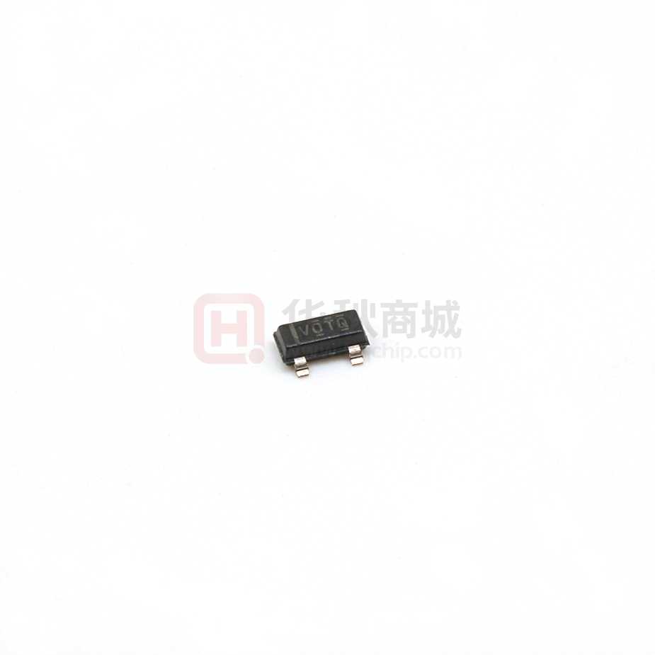
VOUQ
TLV803MDBZT
ACTIVE
SOT-23
DBZ
3
250
Green (RoHS
& no Sb/Br)
CU NIPDAUAG
Level-1-260C-UNLIM
-40 to 125
VOUQ
TLV803RDBZR
ACTIVE
SOT-23
DBZ
3
3000
Green (RoHS
& no Sb/Br)
CU NIPDAUAG
Level-1-260C-UNLIM
-40 to 125
VOSQ
TLV803RDBZT
ACTIVE
SOT-23
DBZ
3
250
Green (RoHS
& no Sb/Br)
CU NIPDAUAG
Level-1-260C-UNLIM
-40 to 125
VOSQ
TLV803SDBZR
ACTIVE
SOT-23
DBZ
3
3000
Green (RoHS
& no Sb/Br)
CU NIPDAUAG
Level-1-260C-UNLIM
-40 to 125
VOTQ
TLV803SDBZT
ACTIVE
SOT-23
DBZ
3
250
Green (RoHS
& no Sb/Br)
CU NIPDAUAG
Level-1-260C-UNLIM
-40 to 125
VOTQ
TLV803ZDBZR
ACTIVE
SOT-23
DBZ
3
3000
Green (RoHS
& no Sb/Br)
CU NIPDAUAG
Level-1-260C-UNLIM
-40 to 125
VORQ
TLV803ZDBZT
ACTIVE
SOT-23
DBZ
3
250
Green (RoHS
& no Sb/Br)
CU NIPDAUAG
Level-1-260C-UNLIM
-40 to 125
VORQ
TLV853MDBZR
ACTIVE
SOT-23
DBZ
3
3000
Green (RoHS
& no Sb/Br)
CU NIPDAU
Level-1-260C-UNLIM
-40 to 125
ZGM4
TLV853MDBZT
ACTIVE
SOT-23
DBZ
3
250
Green (RoHS
& no Sb/Br)
CU NIPDAU
Level-1-260C-UNLIM
-40 to 125
ZGM4
TLV863MDBZR
ACTIVE
SOT-23
DBZ
3
3000
Green (RoHS
& no Sb/Br)
CU NIPDAUAG
Level-1-260C-UNLIM
-40 to 125
VTWM
TLV863MDBZT
ACTIVE
SOT-23
DBZ
3
250
Green (RoHS
& no Sb/Br)
CU NIPDAUAG
Level-1-260C-UNLIM
-40 to 125
VTWM
(1)
The marketing status values are defined as follows:
ACTIVE: Product device recommended for new designs.
LIFEBUY: TI has announced that the device will be discontinued, and a lifetime-buy period is in effect.
NRND: Not recommended for new designs. Device is in production to support existing customers, but TI does not recommend using this part in a new design.
PREVIEW: Device has been announced but is not in production. Samples may or may not be available.
OBSOLETE: TI has discontinued the production of the device.
(2)
RoHS: TI defines "RoHS" to mean semiconductor products that are compliant with the current EU RoHS requirements for all 10 RoHS substances, including the requirement that RoHS substance
do not exceed 0.1% by weight in homogeneous materials. Where designed to be soldered at high temperatures, "RoHS" products are suitable for use in specified lead-free processes. TI may
reference these types of products as "Pb-Free".
RoHS Exempt: TI defines "RoHS Exempt" to mean products that contain lead but are compliant with EU RoHS pursuant to a specific EU RoHS exemption.
Addendum-Page 1
Samples
�PACKAGE OPTION ADDENDUM
www.ti.com
21-Mar-2019
Green: TI defines "Green" to mean the content of Chlorine (Cl) and Bromine (Br) based flame retardants meet JS709B low halogen requirements of