User's Guide
SLVU461 – May 2011
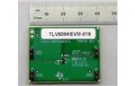
TLV8xxxEVM-019 Evaluation Modules
This user’s guide describes the characteristics, operation, and use of the TLV809K (TLV809KEVM-019),
TLV810S (TLV810SEVM-019), and TLV803S (TLV803SEVM-019) evaluation modules (EVM). The
TLV8xxxEVM is a fully assembled and tested platform for evaluating the performance of the TLV8xxx
family of supervisory circuits. The TLV809K, TLV810S, and TLV803S are single channel, 3-pin, 3.3-V
supply voltage supervisors (SVS) with built-in power-on reset generator with fixed delay time of 200ms.
This user’s guide includes setup configuration instructions, a complete schematic diagram, bill of materials
(BOM), and printed circuit board (PCB) layout drawings for the evaluation module.
1
2
3
4
5
6
Contents
Introduction ..................................................................................................................
Schematic ....................................................................................................................
Setup and Board Description ..............................................................................................
Operation .....................................................................................................................
Board Layout ................................................................................................................
Bill of Materials ..............................................................................................................
1
TLV8xxxEVM Rev A Schematic
1
2
2
3
4
7
List of Figures
2
3
4
5
6
7
..........................................................................................
Quick Start Connection Setup .............................................................................................
Timing Diagram for TLV8xxxEVM ........................................................................................
Silkscreen Layer ............................................................................................................
Assembly Layer .............................................................................................................
Top Layer Routing ..........................................................................................................
Bottom Layer Routing ......................................................................................................
2
3
4
5
5
6
6
List of Tables
1
2
3
1
................................................................
Bill of Materials ..............................................................................................................
Assembly Number and Corresponding Label Text .....................................................................
Threshold voltage, VIT, Values for Each TLV8xxxEVM
4
7
7
Introduction
The TLV8xxxEVM helps designers evaluate the operation and performance of the TLV8xxx family of
single channel supervisors in a 3-pin SOT-23 package. This particular EVM configuration contains a single
SVS capable of supervising up to 6-V supply voltage. The TLV8xxx EVM is assembled with the TLV809K,
TLV810S, or TLV803S, all of which are 3.3-V supply voltage supervisors with threshold voltage, VIT, of
2.93-V. To evaluate the TLV8xxx EVM with a different supply voltage, the IC will need to be replaced. The
TLV8xxx family of supervisory circuits provides initialization and timing supervision, primarily for DSPs and
processor-based systems; and, is available for supply voltages of 2.5-V, 3.0-V, 3.3-V, and 5.0-V.
1.1
Features
•
•
Low supply current: 9 µA (typical)
Power-on RESET / RESET generator with fixed delay time of 200ms
SLVU461 – May 2011
Submit Documentation Feedback
TLV8xxxEVM-019 Evaluation Modules
Copyright © 2011, Texas Instruments Incorporated
1
�Schematic
1.2
Orderable Options
•
•
•
2
www.ti.com
TLV809KEVM-019: 3.3-V single channel supervisor with active low, push-pull RESET output
TLV810SEVM-019: 3.3-V single channel supervisor with active high, push-pull RESET output
TLV803SEVM-019: 3.3-V single channel supervisor with active low, open-drain RESET output
Schematic
Figure 1. TLV8xxxEVM Rev A Schematic
3
Setup and Board Description
3.1
EVM Input/Output Connectors and Test Jumpers
2
Connector
Label
Description
J1
VDD
Input power supply connection: 2V to 6V
J2
GND
Return connection for input power supply
J3
RESET
RESET
J4
GND
JP1
Pull-Up
RESET / RESET output of supervisor IC. Connect this output to a multimeter or oscilloscope to verify
output voltage.
Return connection for output (RESET / RESET)
Necessary for TLV803SEVM-019 only. Placing a jumper on JP1 connects the 49.9kΩ (R1) pull-up
resistor to VDD and RESET output.
TLV8xxxEVM-019 Evaluation Modules
Copyright © 2011, Texas Instruments Incorporated
SLVU461 – May 2011
Submit Documentation Feedback
�Operation
www.ti.com
3.2
Connection Setup
Install jumper
on JP1 for
TLV803S only
A
Power
Supply
V
V
Figure 2. Quick Start Connection Setup
1. Connect the power supply and its return connection to J1 and J2 as shown above.
2. An ammeter can be connected in series with the power supply to measure the supply current. A
voltmeter can also be connected across J1 and J2 to measure the effective voltage at the pins.
3. Connect a voltmeter or an oscilloscope voltage probe across the output pins J3 and J4 to observe and
measure the output voltage.
NOTE: For TLV803SEVM-019, please verify that jumper on JP1 is present so that pull-up resistor
R1 is connected to VDD and to RESET. If an output voltage different from VDD is desired, a
power supply can be connected to JP1 to pull the RESET pin to a different voltage.
4
Operation
This section provides information about the operation of the TLV8xxxEVM and the outputs expected. The
TLV8xxx parts can support supply voltage, VDD, in the range of 2-V to 6-V. No external components are
required. All the devices in this family have a fixed sense-threshold voltage (VIT) set by an internal voltage
divider.
4.1
Threshold Voltage, VIT
During power-on, RESET / RESET is asserted when the supply voltage (VDD) becomes higher than 1.1-V.
Thereafter, for active low devices, the supervisory circuit monitors VDD and keeps RESET active as long
as VDD remains below the threshold voltage, VIT. For active high devices, the supervisory circuit keeps
RESET active as long as VDD remains above the threshold voltage, VIT.
TLV809K and TLV803S (active low RESET output):
• When VDD < VIT, the output across the RESET pins J3 and J4 should be 0-V (low).
• When VDD > VIT, the output across the RESET pins J3 and J4 should equal VDD ± 0.5-V (high) with no
load.
TLV810S (active high RESET output):
• When VDD < VIT, the output across the RESET pins J3 and J4 should equal VDD ± 0.5-V (high) with no
load.
• When VDD > VIT, the output across the RESET pins J3 and J4 should be 0-V (low).
SLVU461 – May 2011
Submit Documentation Feedback
TLV8xxxEVM-019 Evaluation Modules
Copyright © 2011, Texas Instruments Incorporated
3
�Board Layout
www.ti.com
Table 1. Threshold voltage, VIT, Values for Each TLV8xxxEVM
VIT
Part
(1)
4.2
(1)
Min (V)
Typ (V)
Max (V)
TLV809K
2.87
2.93
2.99
TLV810S
2.87
2.93
2.99
TLV803S
2.87
2.93
2.99
VIT values taken from datasheet.
Timing
The TLV8xxx parts have a reset generator with a fixed delay time. An internal timer delays the return of
the output to the inactive state (high) to ensure proper system reset. The delay time (td(typ) = 200ms) starts
after VDD has risen above the threshold voltage, VIT. When the supply voltage, VDD, drops below the VIT
voltage, the output becomes active (low) again. Min and max values for td can be found in the datasheet,
labeled Switching Characteristics.
t d = 211ms
Figure 3. Timing Diagram for TLV8xxxEVM
5
Board Layout
This section provides the TLV8xxxEVM board layout and illustrations.
5.1
Layout
NOTE: Board layouts are not to scale. These figures are intended to show how the board is laid out; they
are not intended to be used for manufacturing TLV8xxx EVM PCBs.
4
TLV8xxxEVM-019 Evaluation Modules
Copyright © 2011, Texas Instruments Incorporated
SLVU461 – May 2011
Submit Documentation Feedback
�Board Layout
www.ti.com
Figure 4. Silkscreen Layer
JP1
EVM P/N
TEXAS INSTRUMENTS
PWR019 REV. A
J3
J1
RESET /RESET
VDD
U1
1
C1
R1
J2
J4
GND
GND
2011
Figure 5. Assembly Layer
SLVU461 – May 2011
Submit Documentation Feedback
TLV8xxxEVM-019 Evaluation Modules
Copyright © 2011, Texas Instruments Incorporated
5
�Board Layout
www.ti.com
Figure 6. Top Layer Routing
Figure 7. Bottom Layer Routing
6
TLV8xxxEVM-019 Evaluation Modules
Copyright © 2011, Texas Instruments Incorporated
SLVU461 – May 2011
Submit Documentation Feedback
�Bill of Materials
www.ti.com
6
Bill of Materials
Table 2. Bill of Materials
PWR019001
PWR019002
PWR019003
COUNT
COUNT
COUNT
1
1
4
4
0
RefDes
Value
Description
Size
Part Number
MFR
1
C1
0.1uF
Capacitor, Ceramic, 10V, X7R, 20%
0603
STD
STD
4
J1, J2, J3,
J4
PEC02SAAN
Header, Male 2-pin, 100mil spacing
0.100 inch x 2
PEC02SAAN
Sullins
0
1
JP1
PEC02SAAN
Header, Male 2-pin, 100mil spacing
0.100 inch x 2
PEC02SAAN
Sullins
0
0
1
R1
49.9k
Resistor, Chip, 1/16W, 1%
0603
STD
STD
1
0
0
U1
TLV809KDBZ
IC, Voltage Supervisors with Active-Low, Push-Pull
RESET
SOT23-3
TLV809K33DBZ
TI
0
1
0
U1
TLV810SDBZ
IC, Voltage Supervisors with Active-High, Push-Pull
RESET
SOT23-3
TLV810SDBZ
TI
0
0
1
U1
TLV803SDBZ
IC, Voltage Supervisors with Active-Low, Open-Drain
RESET
SOT23-3
TLV803SDBZ
TI
0
0
1
–
Shunt, 100-mil, Black
0.1
929950-00
3M
1
1
1
–
Label
1.25 x 0.25 inch
THT-13-457-10
Brady
1
1
1
–
1.645 x 1.300 x 0 .062 inch 2 layer 2oz. PCB
1.645 inch x 1.300 inch
PWR019
Any
PWR019
Notes 1. These assemblies are ESD sensitive, ESD precautions shall be observed.
2. These assemblies must be clean and free from flux and all contaminants. Use of no clean flux is not acceptable.
3. These assemblies must comply with workmanship standards IPC-A-610 Class 2.
4. Ref designators marked with an asterisk ('**') cannot be substituted. All other components can be substituted with equivalent MFG's components.
5. Install label after final wash. Text shall be 8 pt font. Text shall be per Table 3.
Table 3. Assembly Number and Corresponding Label Text
Assembly Number
PWR019-001
PWR019-002
PWR019-003
Text
TLV809KEVM-019
TLV810SEVM-019
TLV803SEVM-019
SLVU461 – May 2011
Submit Documentation Feedback
TLV8xxxEVM-019 Evaluation Modules
Copyright © 2011, Texas Instruments Incorporated
7
�Evaluation Board/Kit Important Notice
Texas Instruments (TI) provides the enclosed product(s) under the following conditions:
This evaluation board/kit is intended for use for ENGINEERING DEVELOPMENT, DEMONSTRATION, OR EVALUATION
PURPOSES ONLY and is not considered by TI to be a finished end-product fit for general consumer use. Persons handling the
product(s) must have electronics training and observe good engineering practice standards. As such, the goods being provided are
not intended to be complete in terms of required design-, marketing-, and/or manufacturing-related protective considerations,
including product safety and environmental measures typically found in end products that incorporate such semiconductor
components or circuit boards. This evaluation board/kit does not fall within the scope of the European Union directives regarding
electromagnetic compatibility, restricted substances (RoHS), recycling (WEEE), FCC, CE or UL, and therefore may not meet the
technical requirements of these directives or other related directives.
Should this evaluation board/kit not meet the specifications indicated in the User’s Guide, the board/kit may be returned within 30
days from the date of delivery for a full refund. THE FOREGOING WARRANTY IS THE EXCLUSIVE WARRANTY MADE BY
SELLER TO BUYER AND IS IN LIEU OF ALL OTHER WARRANTIES, EXPRESSED, IMPLIED, OR STATUTORY, INCLUDING
ANY WARRANTY OF MERCHANTABILITY OR FITNESS FOR ANY PARTICULAR PURPOSE.
The user assumes all responsibility and liability for proper and safe handling of the goods. Further, the user indemnifies TI from all
claims arising from the handling or use of the goods. Due to the open construction of the product, it is the user’s responsibility to
take any and all appropriate precautions with regard to electrostatic discharge.
EXCEPT TO THE EXTENT OF THE INDEMNITY SET FORTH ABOVE, NEITHER PARTY SHALL BE LIABLE TO THE OTHER
FOR ANY INDIRECT, SPECIAL, INCIDENTAL, OR CONSEQUENTIAL DAMAGES.
TI currently deals with a variety of customers for products, and therefore our arrangement with the user is not exclusive.
TI assumes no liability for applications assistance, customer product design, software performance, or infringement of
patents or services described herein.
Please read the User’s Guide and, specifically, the Warnings and Restrictions notice in the User’s Guide prior to handling the
product. This notice contains important safety information about temperatures and voltages. For additional information on TI’s
environmental and/or safety programs, please contact the TI application engineer or visit www.ti.com/esh.
No license is granted under any patent right or other intellectual property right of TI covering or relating to any machine, process, or
combination in which such TI products or services might be or are used.
FCC Warning
This evaluation board/kit is intended for use for ENGINEERING DEVELOPMENT, DEMONSTRATION, OR EVALUATION
PURPOSES ONLY and is not considered by TI to be a finished end-product fit for general consumer use. It generates, uses, and
can radiate radio frequency energy and has not been tested for compliance with the limits of computing devices pursuant to part 15
of FCC rules, which are designed to provide reasonable protection against radio frequency interference. Operation of this
equipment in other environments may cause interference with radio communications, in which case the user at his own expense
will be required to take whatever measures may be required to correct this interference.
EVM Warnings and Restrictions
It is important to operate this EVM within the input voltage range of 2 V to 6 V and the output voltage range of 0 V to 6 V .
Exceeding the specified input range may cause unexpected operation and/or irreversible damage to the EVM. If there are
questions concerning the input range, please contact a TI field representative prior to connecting the input power.
Applying loads outside of the specified output range may result in unintended operation and/or possible permanent damage to the
EVM. Please consult the EVM User's Guide prior to connecting any load to the EVM output. If there is uncertainty as to the load
specification, please contact a TI field representative.
During normal operation, some circuit components may have case temperatures greater than 85° C. The EVM is designed to
operate properly with certain components above 85° C as long as the input and output ranges are maintained. These components
include but are not limited to linear regulators, switching transistors, pass transistors, and current sense resistors. These types of
devices can be identified using the EVM schematic located in the EVM User's Guide. When placing measurement probes near
these devices during operation, please be aware that these devices may be very warm to the touch.
Mailing Address: Texas Instruments, Post Office Box 655303, Dallas, Texas 75265
Copyright © 2011, Texas Instruments Incorporated
�IMPORTANT NOTICE
Texas Instruments Incorporated and its subsidiaries (TI) reserve the right to make corrections, modifications, enhancements, improvements,
and other changes to its products and services at any time and to discontinue any product or service without notice. Customers should
obtain the latest relevant information before placing orders and should verify that such information is current and complete. All products are
sold subject to TI’s terms and conditions of sale supplied at the time of order acknowledgment.
TI warrants performance of its hardware products to the specifications applicable at the time of sale in accordance with TI’s standard
warranty. Testing and other quality control techniques are used to the extent TI deems necessary to support this warranty. Except where
mandated by government requirements, testing of all parameters of each product is not necessarily performed.
TI assumes no liability for applications assistance or customer product design. Customers are responsible for their products and
applications using TI components. To minimize the risks associated with customer products and applications, customers should provide
adequate design and operating safeguards.
TI does not warrant or represent that any license, either express or implied, is granted under any TI patent right, copyright, mask work right,
or other TI intellectual property right relating to any combination, machine, or process in which TI products or services are used. Information
published by TI regarding third-party products or services does not constitute a license from TI to use such products or services or a
warranty or endorsement thereof. Use of such information may require a license from a third party under the patents or other intellectual
property of the third party, or a license from TI under the patents or other intellectual property of TI.
Reproduction of TI information in TI data books or data sheets is permissible only if reproduction is without alteration and is accompanied
by all associated warranties, conditions, limitations, and notices. Reproduction of this information with alteration is an unfair and deceptive
business practice. TI is not responsible or liable for such altered documentation. Information of third parties may be subject to additional
restrictions.
Resale of TI products or services with statements different from or beyond the parameters stated by TI for that product or service voids all
express and any implied warranties for the associated TI product or service and is an unfair and deceptive business practice. TI is not
responsible or liable for any such statements.
TI products are not authorized for use in safety-critical applications (such as life support) where a failure of the TI product would reasonably
be expected to cause severe personal injury or death, unless officers of the parties have executed an agreement specifically governing
such use. Buyers represent that they have all necessary expertise in the safety and regulatory ramifications of their applications, and
acknowledge and agree that they are solely responsible for all legal, regulatory and safety-related requirements concerning their products
and any use of TI products in such safety-critical applications, notwithstanding any applications-related information or support that may be
provided by TI. Further, Buyers must fully indemnify TI and its representatives against any damages arising out of the use of TI products in
such safety-critical applications.
TI products are neither designed nor intended for use in military/aerospace applications or environments unless the TI products are
specifically designated by TI as military-grade or "enhanced plastic." Only products designated by TI as military-grade meet military
specifications. Buyers acknowledge and agree that any such use of TI products which TI has not designated as military-grade is solely at
the Buyer's risk, and that they are solely responsible for compliance with all legal and regulatory requirements in connection with such use.
TI products are neither designed nor intended for use in automotive applications or environments unless the specific TI products are
designated by TI as compliant with ISO/TS 16949 requirements. Buyers acknowledge and agree that, if they use any non-designated
products in automotive applications, TI will not be responsible for any failure to meet such requirements.
Following are URLs where you can obtain information on other Texas Instruments products and application solutions:
Products
Applications
Audio
www.ti.com/audio
Communications and Telecom www.ti.com/communications
Amplifiers
amplifier.ti.com
Computers and Peripherals
www.ti.com/computers
Data Converters
dataconverter.ti.com
Consumer Electronics
www.ti.com/consumer-apps
DLP® Products
www.dlp.com
Energy and Lighting
www.ti.com/energy
DSP
dsp.ti.com
Industrial
www.ti.com/industrial
Clocks and Timers
www.ti.com/clocks
Medical
www.ti.com/medical
Interface
interface.ti.com
Security
www.ti.com/security
Logic
logic.ti.com
Space, Avionics and Defense
www.ti.com/space-avionics-defense
Power Mgmt
power.ti.com
Transportation and
Automotive
www.ti.com/automotive
Microcontrollers
microcontroller.ti.com
Video and Imaging
www.ti.com/video
RFID
www.ti-rfid.com
Wireless
www.ti.com/wireless-apps
RF/IF and ZigBee® Solutions
www.ti.com/lprf
TI E2E Community Home Page
e2e.ti.com
Mailing Address: Texas Instruments, Post Office Box 655303, Dallas, Texas 75265
Copyright © 2011, Texas Instruments Incorporated
�