TMAG5231
SLYS042D – AUGUST 2021 – REVISED SEPTEMBER 2022
TMAG5231 Low-Power, Hall Effect Switch
1 Features
3 Description
•
The TMAG5231 is a 2nd-generation, low-power Halleffect switch sensor, specifically designed to optimize
the total system cost for compact, battery-operated
consumer and industrial applications.
•
•
•
•
•
•
Low power consumption:
– 10-Hz versions: 1.3 µA at 3 V
– 20-Hz versions: 2 µA at 3 V
– 216-Hz versions: 16 µA at 3 V
1.65-V to 5.5-V operating VCC range
Magnetic threshold option (typical BOP):
– 1.8 mT with 0.6-mT hysteresis
– 2.85 mT with 1.35-mT hysteresis
– 3 mT with 0.8-mT hysteresis
– 40 mT with 6.5-mT hysteresis
Omnipolar response
Push-pull output
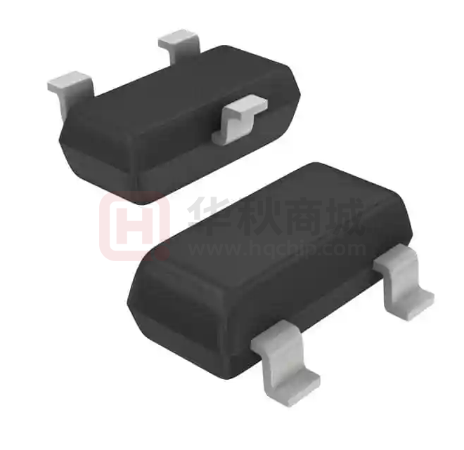
Industry-standard package and pinout
– SOT-23 package
– X2SON package
Operating temperature range: –40°C to +125°C
2 Applications
•
•
•
•
•
•
•
•
•
Cell phones, laptops, or tablet case sensing
Electricity meter tamper detection
E-locks
Smoke detectors
Home appliance open/close detection
Medical devices
IoT systems
Valve and solenoid position detection
Contactless diagnostics or activation
When the applied magnetic flux density exceeds the
operating point (BOP) threshold, the device outputs a
low voltage. The output stays low until the flux density
decreases to less than the release point (BRP), and
then the device outputs a high voltage. Omnipolar
magnetic response allows the output to be sensitive
to both north and south magnetic fields.
The TMAG5231 is able to operate at very low current
consumption. To achieve 2 μA of current consumption
the device is internally power cycled at a 20-Hz rate.
The TMAG5231 is available in the industry-standard
package and pinout SOT-23 as well as X2SON.
The device operates at a VCC range of 1.65 V to 5.5 V
as well as an extended temperature range of –40°C to
125°C.
Package Information(1)
PART NUMBER
TMAG5231
(1)
PACKAGE
BODY SIZE (NOM)
SOT-23 (3)
2.92 mm × 1.30 mm
X2SON (4)
1.10 mm × 1.40 mm
For all available packages, see the orderable addendum at
the end of the data sheet.
VCC
VCC
LDO
X
Low-Power
Oscillator
Amp
OUT
Output
control
Chopper
stabiliza on
GND
Block Diagram
An IMPORTANT NOTICE at the end of this data sheet addresses availability, warranty, changes, use in safety-critical applications,
intellectual property matters and other important disclaimers. PRODUCTION DATA.
�TMAG5231
www.ti.com
SLYS042D – AUGUST 2021 – REVISED SEPTEMBER 2022
Table of Contents
1 Features............................................................................1
2 Applications..................................................................... 1
3 Description.......................................................................1
4 Revision History.............................................................. 2
5 Device Comparison......................................................... 3
6 Pin Configuration and Functions...................................3
7 Specifications.................................................................. 4
7.1 Absolute Maximum Ratings........................................ 4
7.2 ESD Ratings............................................................... 4
7.3 Recommended Operating Conditions.........................4
7.4 Thermal Information....................................................4
7.5 Electrical Characteristics.............................................5
7.6 Magnetic Characteristics.............................................5
7.7 Typical Characteristics................................................ 6
8 Detailed Description........................................................8
8.1 Overview..................................................................... 8
8.2 Functional Block Diagram........................................... 8
8.3 Feature Description.....................................................8
8.4 Device Functional Modes..........................................11
9 Application and Implementation.................................. 12
9.1 Application Information............................................. 12
9.2 Typical Applications.................................................. 14
9.3 Power Supply Recommendations.............................19
9.4 Layout....................................................................... 19
10 Device and Documentation Support..........................21
10.1 Support Resources................................................. 21
10.2 Trademarks............................................................. 21
10.3 Electrostatic Discharge Caution..............................21
10.4 Glossary..................................................................21
11 Mechanical and Packaging Information.................... 21
4 Revision History
NOTE: Page numbers for previous revisions may differ from page numbers in the current version.
Changes from Revision C (June 2022) to Revision D (September 2022)
Page
• Changed Device Information table to Package Information .............................................................................. 1
• Changed the package information in Device Comparison table.........................................................................3
• Moved the Power Supply Recommendations and Layout sections to the Application and Implementation
section.............................................................................................................................................................. 19
Changes from Revision B (March 2022) to Revision C (June 2022)
Page
• Changed data sheet status from Production Mixed to Production Data............................................................. 1
• Added Additional Magnetic Threshold option to Features section......................................................................1
• Added TMAG5231A1C TMAG5231A2D, and TMAG5231C1D to Device Comparison table.............................3
• Added TMAG5231xxC to Electrical Characteristics table...................................................................................5
• Added TMAG5231Axx to the Magnetic Characteristics table.............................................................................5
Changes from Revision A (November 2021) to Revision B (March 2022)
Page
• Changed data sheet status from Production Data to Production Mixed............................................................. 1
• Added Advanced Information DMR (X2SON) package to the data sheet.......................................................... 1
• Changed the Device Comparison table.............................................................................................................. 3
Changes from Revision * (August 2021) to Revision A (November 2021)
Page
• Changed data sheet status from Advanced Information to Production Data......................................................1
• Added the FA and FD device versions............................................................................................................... 1
2
Submit Document Feedback
Copyright © 2022 Texas Instruments Incorporated
Product Folder Links: TMAG5231
�TMAG5231
www.ti.com
SLYS042D – AUGUST 2021 – REVISED SEPTEMBER 2022
5 Device Comparison
Table 5-1. Device Comparison
VERSION
TYPICAL
THRESHOLD
TYPICAL
HYSTERESIS
MAGNETIC
RESPONSE
OUTPUT
TYPE
SENSOR
ORIENTATION
SAMPLING
RATE
PACKAGES
AVAILABLE
TMAG5231A1C
1.8 mT
0.6 mT
Omnipolar
active Low
Push-pull
Z
10 Hz
SOT-23
X2SON
TMAG5231A2D
1.8 mT
0.6 mT
Omnipolar
active High
Push-pull
Z
20 Hz
SOT-23
X2SON
TMAG5231B1D
2.85 mT
1.35 mT
Omnipolar
active Low
Push-pull
Z
20 Hz
SOT-23
X2SON
TMAG5231C1D
3 mT
0.8 mT
Omnipolar
active Low
Push-pull
Z
20 Hz
SOT-23
X2SON
TMAG5231C1G
3 mT
0.8 mT
Omnipolar
active Low
Push-pull
Z
216 Hz
SOT-23
X2SON
TMAG5231H1D
40 mT
6.5 mT
Omnipolar
active Low
Push-pull
Z
20 Hz
SOT-23
X2SON
6 Pin Configuration and Functions
VCC
1
OUT
VCC
1
4
Thermal
Pad
GND
3
GND
2
2
3
OUT
NC
Figure 6-2. DMR Package 4-Pin X2SON Top View
Figure 6-1. DBZ Package 3-Pin SOT-23 Top View
Table 6-1. Pin Functions
PIN
NAME
GND
OUT
VCC
I/O
X2SON (4)
3
1
—
Ground reference
2
3
O
Omnipolar output that responds to north and south magnetic
poles
1
4
—
1.65-V to 5.5-V power supply. TI recommends connecting this pin
to a ceramic capacitor to ground with a value of at least 0.1 µF.
—
2
—
No connect. This pin is not connected to the silicon. It should be
left floating or tied to ground. It should be soldered to the board
for mechanical support.
—
PAD
—
No connect. This pin should be left floating or tied to ground. It
should be soldered to the board for mechanical support.
NC
Thermal Pad
DESCRIPTION
SOT-23 (3)
Submit Document Feedback
Copyright © 2022 Texas Instruments Incorporated
Product Folder Links: TMAG5231
3
�TMAG5231
www.ti.com
SLYS042D – AUGUST 2021 – REVISED SEPTEMBER 2022
7 Specifications
7.1 Absolute Maximum Ratings
over operating free-air temperature range (unless otherwise noted)(1)
MIN
Power Supply Voltage
VCC
Output Pin Voltage
OUT
Output Pin current
OUT
–0.3
5.5
GND – 0.3
VCC + 0.3
–5
5
Magnetic Flux Density, BMAX
Junction temperature, TJ
UNIT
V
mA
Unlimited
T
Junction temperature, TJ
Storage temperature, Tstg
(1)
MAX
–65
150
°C
150
°C
Operation outside the Absolute Maximum Ratings may cause permanent device damage. Absolute Maximum
Ratings do not imply functional operation of the device at these or any other conditions beyond those listed
under Recommended Operating Conditions. If used outside the Recommended Operating Conditions but within
the Absolute Maximum Ratings, the device may not be fully functional, and this may affect device reliability,
functionality, performance, and shorten the device lifetime.
7.2 ESD Ratings
VALUE
V(ESD)
(1)
(2)
Electrostatic discharge
Human body model (HBM), per ANSI/ESDA/
JEDEC JS-001, all pins(1)
±5500
Charged device model (CDM), per ANSI/ESDA/
JEDEC JS-002, all pins(2)
± 500
UNIT
V
JEDEC document JEP155 states that 500-V HBM allows safe manufacturing with a standard ESD control process.
JEDEC document JEP157 states that 250-V CDM allows safe manufacturing with a standard ESD control process.
7.3 Recommended Operating Conditions
over operating free-air temperature range (unless otherwise noted)
MIN
MAX
1.65
5.5
Output voltage
0
5.5
Output current
–5
5
mA
–40
125
°C
VCC
Power supply voltage
Vo
Io
TA
Ambient temperature
UNIT
V
V
7.4 Thermal Information
THERMAL METRIC(1)
TMAG5231
X2SON (DMR)
3 PINS
4 PINS
RθJA
Junction-to-ambient thermal resistance
227.4
218.4
RθJC(top)
Junction-to-case (top) thermal resistance
122.7
174.1
RθJB
Junction-to-board thermal resistance
61.2
172.4
ΨJT
Junction-to-top characterization parameter
21.3
11.9
ΨJB
Junction-to-board characterization parameter
60.8
167.2
RθJC(bot)
Junction-to-case (bottom) thermal resistance
N/A
144.9
(1)
4
TMAG5231
SOT-23 (DBZ)
UNIT
°C/W
For more information about traditional and new thermal metrics, see the Semiconductor and IC Package Thermal Metrics application
report.
Submit Document Feedback
Copyright © 2022 Texas Instruments Incorporated
Product Folder Links: TMAG5231
�TMAG5231
www.ti.com
SLYS042D – AUGUST 2021 – REVISED SEPTEMBER 2022
7.5 Electrical Characteristics
for VCC = 1.65 V to 5.5 V, over operating free-air temperature range (unless otherwise noted)
PARAMETER
TEST CONDITIONS
MIN
TYP
Vcc-0.35
Vcc-0.1
MAX
UNIT
PUSH-PULL OUTPUT DRIVER
VOH
High-level output voltage
IOUT = -0.5 mA
VOL
Low-level output voltage
IOUT = 0.5 mA
V
0.1
0.3
V
136
216
374
Hz
2.67
4.63
7.35
ms
TMAG5231xxG
fs
Frequency of magnetic sampling
ts
Period of magnetic sampling
ICC(AVG)
Average current consumption
Vcc = 3 V over temperature
16
µA
TMAG5231xxD
fs
Frequency of magnetic sampling
ts
Period of magnetic sampling
ICC(AVG)
Average current consumption
13
20
29
50
Vcc = 3 V over temperature
Hz
ms
2
3
µA
7
10
14.5
Hz
77
100
143
ms
TMAG5231xxC
fs
Frequency of magnetic sampling
ts
Period of magnetic sampling
ICC(AVG)
Average current consumption
Vcc = 3 V over temperature
1.3
µA
ALL VERSIONS
ICC(PK)
Peak current consumption
0.8
1.25
ICC(SLP)
Sleep current consumption
tON
tACTIVE
2
mA
Power-on time
65
0.8
1.4
µA
140
425
Active time period
45
60
75
MIN
TYP
MAX
UNIT
±0.9
±1.8
±2.7
mT
±0.3
±1.2
±2.2
mT
±0.1
±0.6
±1.4
mT
±1.9
±2.85
±3.8
±0.5
±1.5
±2.5
±0.5
±1.35
±2.2
µs
7.6 Magnetic Characteristics
for VCC = 1.65 V to 5.5 V
PARAMETER
TEST CONDITIONS
TMAG5231Axx
BOP
Magnetic threshold operate point
BRP
Magnetic release operate point
BHYS
Magnetic hysteresis
Temperature = 25 °C
TMAG5231B1D
BOP
Magnetic threshold operate point
BRP
Magnetic release operate point
BHYS
Magnetic hysteresis
Temperature = 25 °C
mT
TMAG5231Cxx
BOP
Magnetic threshold operate point
BRP
Magnetic release operate point
BHYS
Magnetic hysteresis
Temperature = 25 °C
±2
±3
±4
±1.2
±2.2
±3.2
±0.3
±0.8
±1.5
mT
TMAG5231H1D
BOP
Magnetic threshold operate point
BRP
Magnetic release operate point
BHYS
Magnetic hysteresis
Temperature = 25 °C
±30
±40
±50
±23.5
±33.5
±43.5
±4.5
±6.5
±8.5
mT
Submit Document Feedback
Copyright © 2022 Texas Instruments Incorporated
Product Folder Links: TMAG5231
5
�TMAG5231
www.ti.com
SLYS042D – AUGUST 2021 – REVISED SEPTEMBER 2022
7.7 Typical Characteristics
2.5
2.5
BOPN
BRPS
1.5
0.5
-0.5
-1.5
-2.5
-40
BOPS
BRPN
Magnetic Threshold (mT)
Magnetic Threshold (mT)
BOPS
-25
-10
5
20 35 50 65
Temperature (C)
80
95
-0.5
-1.5
2.65
3.65
Supply Voltage (V)
5.5
Figure 7-2. 1.8 mT Threshold vs. Supply Voltage
5
5
BOPS
BOPN
BRPS
BOPS
BRPN
3
Magnetic Threshold (mT)
Magnetic Threshold (mT)
4.65
TA = 25°C
Figure 7-1. 1.8 mT Threshold vs. Temperature
1
-1
-3
-25
-10
5
20 35 50 65
Temperature (C)
80
95
BRPS
BRPN
1
-1
-3
-5
1.65
110 125
BOPN
3
2.65
3.65
Supply Voltage (V)
4.65
5.5
TA = 25°C
VCC = 3 V
Figure 7-3. 2.85 mT Threshold vs. Temperature
Figure 7-4. 2.85 mT Threshold vs. Supply Voltage
5
5
BOPS
BOPN
BRPS
BRPN
3
4
Magnetic Threshold (mT)
Magnetic Threshold (mT)
BRPN
0.5
VCC = 3 V
-5
-40
BRPS
1.5
-2.5
1.65
110 125
BOPN
1
-1
-3
BOPS
BOPN
BRPS
BRPN
3
2
1
0
-1
-2
-3
-4
-5
-40
-25
-10
5
20 35 50 65
Temperature (C)
80
95
110 125
-5
1.65
3.65
Supply Voltage (V)
4.65
5.5
TA = 25°C
VCC = 3 V
Figure 7-5. 3.0 mT Threshold vs. Temperature
6
2.65
Figure 7-6. 3.0 mT Threshold vs. Supply Voltage
Submit Document Feedback
Copyright © 2022 Texas Instruments Incorporated
Product Folder Links: TMAG5231
�TMAG5231
www.ti.com
SLYS042D – AUGUST 2021 – REVISED SEPTEMBER 2022
4
4
3
VCC = 1.65 V
VCC = 3 V
VCC = 5.5 V
Supply Current (A)
Supply Current (A)
VCC = 1.65 V
VCC = 3 V
VCC = 5.5 V
2
1
0
-40
-25
-10
5
20 35 50 65
Temperature (C)
80
95
3
2
1
0
-40
110 125
-25
Magnetic Threshold = 1.8 mT
Sampling Rate = 10 Hz
-10
5
20 35 50 65
Temperature (C)
80
110 125
Magnetic Threshold = 1.8 mT
Sampling Rate = 20 Hz
Figure 7-7. ICC vs. Temperature
Figure 7-8. ICC vs. Temperature
4
4
VCC = 1.65 V
VCC = 3 V
VCC = 5.5 V
3
VCC = 1.65 V
VCC = 3 V
VCC = 5.5 V
Supply Current (A)
Supply Current (A)
95
2
1
0
-40
-25
-10
5
20 35 50 65
Temperature (C)
80
95
3
2
1
0
-40
110 125
-25
Magnetic Threshold = 2.85 mT
Sampling Rate = 20 Hz
-10
5
20 35 50 65
Temperature (C)
80
95
110 125
Magnetic Threshold = 3.0 mT
Sampling Rate = 20 Hz
Figure 7-9. ICC vs. Temperature
Figure 7-10. ICC vs. Temperature
4
Supply Current (A)
VCC = 1.65 V
VCC = 3 V
VCC = 5.5 V
3
2
1
0
-40
-25
Magnetic Threshold = 3.0 mT
Sampling Rate = 216 Hz
-10
5
20 35 50 65
Temperature (C)
80
95
110 125
Magnetic Threshold = 40 mT
Sampling Rate = 20 Hz
Figure 7-11. ICC vs. Temperature
Figure 7-12. ICC vs. Temperature
Submit Document Feedback
Copyright © 2022 Texas Instruments Incorporated
Product Folder Links: TMAG5231
7
�TMAG5231
www.ti.com
SLYS042D – AUGUST 2021 – REVISED SEPTEMBER 2022
8 Detailed Description
8.1 Overview
The TMAG5231 device is a magnetic sensor with a digital output that indicates when the magnetic flux density
threshold has been crossed. The output consists of a push-pull turning low when a field is present or turning
high when no field is present. As an omnipolar switch the output is sensitive to both the South and the North
Pole. The device integrates a Hall Effect element, analog signal conditioning, and a low-frequency oscillator
that enables ultra-low average power consumption. To achieve low-power consumption the device periodically
measures magnetic flux density, updates the output, and enters into a low-power sleep state. With a supply
range of 1.65 V to 5.5 V, this device is designed for battery-operated applications.
8.2 Functional Block Diagram
VCC
VCC
Low-Power
Oscillator
LDO
X
OUT
Output
control
Amp
Chopper
stabiliza on
GND
8.3 Feature Description
8.3.1 Magnetic Flux Direction
Figure 8-1 shows that the TMAG5231 device is sensitive to the magnetic field component that is perpendicular to
the top of the package.
B
B
SOT-23
X2SON
PCB
Figure 8-1. Direction of Sensitivity
Magnetic flux that travels from the bottom to the top of the package is considered positive in this data sheet. This
condition exists when a south magnetic pole is near the top of the package. Magnetic flux that travels from the
top to the bottom of the package results in negative millitesla values.
8
Submit Document Feedback
Copyright © 2022 Texas Instruments Incorporated
Product Folder Links: TMAG5231
�TMAG5231
www.ti.com
SLYS042D – AUGUST 2021 – REVISED SEPTEMBER 2022
positive B
negative B
N
S
S
N
PCB
PCB
Figure 8-2. Flux Direction Polarity
8.3.2 Magnetic Response
The TMAG5231 is an omnipolar switch. Figure 8-3 shows the output responds to both north and south poles.
OUT
BHYS
BHYS
VCC
0V
north
BOP BRP
0 mT
B
BRP BOP
south
Figure 8-3. Omnipolar Functionality
Submit Document Feedback
Copyright © 2022 Texas Instruments Incorporated
Product Folder Links: TMAG5231
9
�TMAG5231
www.ti.com
SLYS042D – AUGUST 2021 – REVISED SEPTEMBER 2022
8.3.3 Output Type
The TMAG5231 has a push-pull CMOS output that can drive the output voltage near VCC or ground level.
VCC
Output
Control
Output
Figure 8-4. Push-Pull Output (Simplified)
8.3.4 Sampling Rate
When the TMAG5231 powers up, the device measures the first magnetic sample and sets the output within the
tON time. The output is latched, and the device enters an ultra low power sleep state. After each tS time has
passed, the device measures a new sample and updates the output if necessary. If the magnetic field does not
change between periods, the output also does not change.
VCC
1.65 V
tON
time
tS
ICC
tS
tACTIVE
ICC(PK)
time
Output
VCC
Invalid
1st sample
2nd sample
3rd sample
GND
time
Figure 8-5. Timing Diagram
10
Submit Document Feedback
Copyright © 2022 Texas Instruments Incorporated
Product Folder Links: TMAG5231
�TMAG5231
www.ti.com
SLYS042D – AUGUST 2021 – REVISED SEPTEMBER 2022
8.3.5 Hall Element Location
The sensing element inside the device is in the center of both packages when viewed from the top. Figure 8-6
shows the tolerances and side-view dimensions.
SOT-23
Top View
SOT-23
Side View
centered
650 µm
±70 µm
±80 µm
X2SON
Top View
X2SON
Side View
centered
250 µm
±60 µm
±50 µm
Figure 8-6. Hall Element Location
8.4 Device Functional Modes
The TMAG5231 device has one mode of operation that applies when the Recommended Operating Conditions
are met.
Submit Document Feedback
Copyright © 2022 Texas Instruments Incorporated
Product Folder Links: TMAG5231
11
�TMAG5231
www.ti.com
SLYS042D – AUGUST 2021 – REVISED SEPTEMBER 2022
9 Application and Implementation
Note
Information in the following applications sections is not part of the TI component specification,
and TI does not warrant its accuracy or completeness. TI’s customers are responsible for
determining suitability of components for their purposes, as well as validating and testing their design
implementation to confirm system functionality.
9.1 Application Information
The TMAG5231 device is typically used to detect the proximity of a magnet. The magnet is often attached to a
movable component in the system.
9.1.1 Defining the Design Implementation
The first step of design is identifying your general design implementation, which means you will define whether
you are detecting a magnet sliding past the sensor, moving head-on toward the sensor, or swinging toward the
sensor on a hinge. Figure 9-1 shows examples for each of the aforementioned design implementations.
Figure 9-1. Design Implementations
With each implementation, the objective is to design the system such that the spatial coordinates of the transition
region fall within the spatial coordinates associated with the BOP maximum and BRP minimum specifications.
Figure 9-2 shows a head-on example that shows how the location corresponding to the device BOPMAX
and BRPMIN fall within the desired transition region. To facilitate rapid design iteration, TI’s Magnetic Sensing
Proximity Tool is leveraged in the following design examples.
12
Submit Document Feedback
Copyright © 2022 Texas Instruments Incorporated
Product Folder Links: TMAG5231
�TMAG5231
www.ti.com
SLYS042D – AUGUST 2021 – REVISED SEPTEMBER 2022
Figure 9-2. Head-On Example
Submit Document Feedback
Copyright © 2022 Texas Instruments Incorporated
Product Folder Links: TMAG5231
13
�TMAG5231
www.ti.com
SLYS042D – AUGUST 2021 – REVISED SEPTEMBER 2022
9.2 Typical Applications
9.2.1 Hinge
XZ-Plane Displacement Dimensions
*Dimensions not to scale
XY-Plane Displacement Dimensions
*Dimensions not to scale
*Magnet offsets when magnet oriented at 0°
Figure 9-3. Typical Application Diagram
9.2.1.1 Design Requirements
Table 9-1 lists the design parameters for this example.
Table 9-1. Design Parameters
DESIGN PARAMETER
14
EXAMPLE VALUE
VCC
3.3 V
Switch Region
5° to 15°
Max Magnet
1/4" ( 6.35 mm)
Max Magnet Width or Length
1" (25.4 mm)
Fixture Width
12" (304.8 mm)
Fixture Length
9" (228.6 mm)
Sensor Distance From Hing Origin
0.23622" (6 mm)
Center Of Magnet Offset From Hinge Origin
≥(6 mm – Magnet Height/2)
Submit Document Feedback
Copyright © 2022 Texas Instruments Incorporated
Product Folder Links: TMAG5231
�TMAG5231
www.ti.com
SLYS042D – AUGUST 2021 – REVISED SEPTEMBER 2022
9.2.1.2 Detailed Design Procedure
Due to the complex non-linear behavior magnets and the number of variables that can influence it, some
experimentation is required to solve for a design that will work. This application uses a simple axial, dipole, block
magnet. Other shapes might be considered for different field strengths or prices. A neodymium type of magnet
(N52) is used. At the time of this writing, N52 can be commonly found with heights of 1/16", 1/8", 3/16", and 1/4".
As price often increases with size, the first design attempt will be with a 1/16" thick magnet, which has a width
and length equal to 0.25". Based on the sensor distance from hinge origin and fixture dimension constraints,
there is a lot of flexibility on where the sensor can be placed. Due to other hardware within the fixture, the
TMAG5231B1DQDBZ sensor is placed 8" (203.2 mm) from the origin. From there, the user can assess a design
with the following displacement dimensions.
Figure 9-4 shows that the b-field magnitude for the TMAG5231B1DQDBZ is not adequate for the spatial
constraints of 5° and 15°, as the Bz magnitude only surpasses the BRP minimum. There are a few options
on how to proceed. As the BOP(Max) does not fall within our range,the user must increase field strength. This can
be accomplished with a thicker magnet or by adjusting sensor and magnet z-offsets. The magnet cannot get any
closer due to enclosure constraints, therefore the only option allowed is to increase the magnet thickness. After a
few more iterations with the tool, a 0.25" × 0.25" × 0.25" magnet can work (see Figure 9-5 and Figure 9-6).
9.2.1.3 Application Curves
Figure 9-4. B-Field Hypothesis One
Figure 9-5. B-Field Hypothesis Two
Figure 9-6. Thresholds
Submit Document Feedback
Copyright © 2022 Texas Instruments Incorporated
Product Folder Links: TMAG5231
15
�TMAG5231
www.ti.com
SLYS042D – AUGUST 2021 – REVISED SEPTEMBER 2022
9.2.2 Head-On
XZ-Plane Displacement Dimensions
*Dimensions not to scale
XY-Plane Displacement Dimensions
*Dimensions not to scale
Figure 9-7. Typical Application Diagram
9.2.2.1 Design Requirements
Table 9-1 lists the design parameters for this example.
Table 9-2. Design Parameters
DESIGN PARAMETER
16
EXAMPLE VALUE
VCC
3.3 V
Switch Region
Between 10 mm and 30 mm from
sensor fixture Surface
Sensor Distance From Equipment Outer Surface
0.0787" (2 mm)
Magnet Length


 工商网监
湘ICP备2023018690号
工商网监
湘ICP备2023018690号
