User's Guide
SPRUHW2 – June 2019
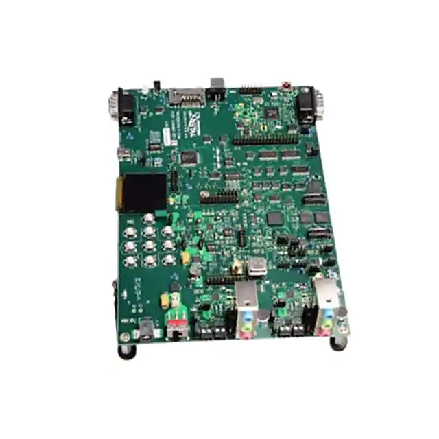
C5517 Evaluation Module (EVM)
This user's guide describes the hardware architecture of the C5517 Evaluation Module (TMDSEVM5517).
1
2
3
4
5
6
7
8
9
Contents
About C5517 ................................................................................................................. 2
EVM Support Page .......................................................................................................... 2
Hardware Configuration ..................................................................................................... 2
I/O Mux Configuration ....................................................................................................... 5
Software and IDE Configuration ........................................................................................... 6
C5517 Boot-Image Programmer ........................................................................................... 9
Common Mistakes in Boot Image User Code .......................................................................... 12
C5517 Jumpers and Switches ............................................................................................ 13
References .................................................................................................................. 16
List of Tables
1
2
3
4
5
6
7
8
9
10
........................................................................................................................... 2
Clock Selection Options .................................................................................................... 3
Boot Mode Configuration Options ......................................................................................... 3
SW 5........................................................................................................................... 4
SW 6........................................................................................................................... 4
CPU VCC Core Configuration ............................................................................................. 4
SW4 ........................................................................................................................... 5
MMC1/McSPI Mux Options................................................................................................. 5
SW11 .......................................................................................................................... 6
C5517 Jumpers and Switches ............................................................................................ 13
SW3
Trademarks
All trademarks are the property of their respective owners.
SPRUHW2 – June 2019
Submit Documentation Feedback
C5517 Evaluation Module (EVM)
Copyright © 2019, Texas Instruments Incorporated
1
�About C5517
1
www.ti.com
About C5517
C5517 device is a member of TI's C5000 fixed-point Digital Signal Processor (DSP) product family and is
designed for low active and standby power consumption. For more information on this device and to view
data sheet and technical reference manual, visit the product folder page:
http://www.ti.com/product/TMS320C5517.
2
EVM Support Page
Spectrum Digital 5517 EVM Support Page (includes schematics, technical reference, BOM, BSL, and so
forth).
3
Hardware Configuration
3.1
Quick Start Guide
For quick configuration and out of the box experience, see the Quick Start Guide that ships with the EVM
[2].
3.2
Boot Mode Configuration
C5517 general purpose EVM is a robust, configurable platform that can be used with different boot
modes. Switch #3 (SW3) is responsible for configuring the boot mode using 8 options.
Table 1. SW3
Name
Description
BOOTMODE0
BOOTMODE[3:0] combine to select the
boot source - see table, shared with
GP[21]/EMIF_A[15]
OFF
ON = 1 (high), OFF = 0 (low) - see
Table 2
BOOTMODE1
BOOTMODE[3:0] combine to select the
boot source - see table, shared with
GP[22]/EMIF_A[16]
OFF
ON = 1 (high), OFF = 0 (low) - see
Table 2
BOOTMODE2
BOOTMODE[3:0] combine to select the
boot source - see table, shared with
GP[23]/EMIF_A[17]
OFF
ON = 1 (high), OFF = 0 (low) - see
Table 2
BOOTMODE3
BOOTMODE[3:0] combine to select the
boot source - see table, shared with
GP[24]/EMIF_A[18]
OFF
ON = 1 (high), OFF = 0 (low) - see
Table 2
BOOTMODE4
BOOTMODE[5:4] combine to define CLK
source for bootloader timings - see table,
shared with GP[25]/EMIF_A[19]
ON
ON = 1 (high), OFF = 0 (low) - see
Table 2
BOOTMODE5
BOOTMODE[5:4] combine to define CLK
source for bootloader timings - see table,
shared with GP[26]/EMIF_A[20]
OFF
ON = 1 (high), OFF = 0 (low) - see
Table 2
NOT USED
Not used
OFF
BOOTM_PULSE_SOURCE
ON: BOOTMODE pins asserted for ~200
µS delay after RESET, OFF: MSP430
asserts BOOTMODE pins
ON
2
Default
C5517 Evaluation Module (EVM)
Default Explained/Useful Info
BOOTMODE pins asserted only during
boot, then Hi-Z so pins can be used as
EMIF or GPIO. BOOTMODE pins driven
when U13 OEn = LOW,
BOOTM_PULSE_SOURCE selects
OEn source. MSP430 held in reset by
default, use delayed reset.
SPRUHW2 – June 2019
Submit Documentation Feedback
Copyright © 2019, Texas Instruments Incorporated
�Hardware Configuration
www.ti.com
Pins 3:0 define the actual boot mode and pins 5:4 define the clocking.
Table 2. Clock Selection Options
SW3 Pins
Value
BootMode [5:4]
00
Description
CLK_SEL = 0: 12 MHz via the on-chip USB oscillator
CLK_SEL = 1: 11.2896 MHz via the CLK_IN pin
01
CLK_SEL = 0: 12 MHz via the on-chip USB oscillator
CLK_SEL = 1: 12.00 MHz or 12.288 MHz via the CLK_IN pin
10
CLK_SEL = 0: 12 MHz via the on-chip USB oscillator
CLK_SEL = 1: 16.8 MHz via the CLK_IN pin
11
CLK_SEL = 0: 12 MHz via the on-chip USB oscillator
CLK_SEL = 1: 19.2 MHz via the CLK_IN pin
Table 3. Boot Mode Configuration Options
SW3 Pins
Value
Description
0000
Boot mode: 16-bit NOR flash data boot, system clock generator is in bypass mode.
0001
Boot mode: 16-bit or 8-bit NAND flash data boot, system clock generator is in bypass
mode.
0010
Boot mode: UART 9600 baud boot, system clock generator output = input clock x 3
0011
Boot mode: UART 57600 baud boot, system clock generator output = input clock x 3
0100
Boot mode: UART 115200 baud boot, system clock generator output = input clock x 3
0101
Boot mode: SPI 16-bit or 24-bit address Boot (SPI_CLK < 1 MHz), system clock
generator output = input clock x 3
0110
Boot mode: SPI 16-bit or 24-bit address Boot (SPI_CLK < 10 MHz), system clock
generator output = input clock x 3
0111
Polling Mode 2: Check for valid boot image from peripherals in the following order: NOR,
NAND, SPI, I2C, SD/SDHC/MMC/eMMC Controller 0, McSPI, and UART/USB (infinite
retry).(2)
1000
Boot mode: I2C 16-bit address Boot, 400 kHz, system clock generator is in bypass mode.
1001
Boot mode: SD or SDHC, MMC, or eMMC Controller 0 card boot, system clock generator
is in bypass mode
1010
Boot mode: SD or SDHC, MMC, or eMMC Controller 1 card boot, system clock generator
is in bypass mode
1011
Polling Mode 1: Check for valid boot image from peripherals in the following order: NOR,
NAND, SPI, I2C, SD/SDHC/MMC/eMMC Controller 0, SD/SDHC/MMC/eMMC Controller
1, and UART/USB (infinite retry).(2)
1100
Boot mode: UHPI 16-bit multiplexed mode boot, system clock generator output = input
clock x 3
1101
Boot mode: McSPI 24-bit address serial flash at 10-MHz mode
1110
Boot mode: McSPI 24-bit address serial flash at 40-MHz mode
1111
Boot mode: USB boot, system clock generator output = input clock x 3
BootMode [3:0]
SPRUHW2 – June 2019
Submit Documentation Feedback
C5517 Evaluation Module (EVM)
Copyright © 2019, Texas Instruments Incorporated
3
�Hardware Configuration
3.3
www.ti.com
Power Configuration
Similar to boot modes, the power is very configurable on the EVM. The configuration is primarily driven by
SW 5 and 6 described in Table 4 and Table 5.
3.4
SW5
Table 4. SW 5
Number
Description
1
EN LDO_1V3/IO1
TPS65023 LDO_EN - ON = HIGH = LDOs enabled,
LDO1 supplies
V1.3, LDO2 supplies VDD_IO1
ON
Connected to MSP430
P5.7/TB0.1 (software
override)
2
EN VCC_3V3
TPS65023 DCDC3_EN - ON = HIGH = DCDC3
enabled, supplies V3.3
ON
Connected to MSP430
P5.6/TB0.0 (software
override)
3
EN VCC_1V8
TTPS65023 DCDC2_EN - ON = HIGH = DCDC2
enabled, supplies V1.8 & VDD_IO2 (EMIF)
ON
Connected to MSP430
P4.7/PM_NONE (software
override)
4
EN CPU_CORE
TPS65023 DCDC1_EN - ON = HIGH = DCDC1
enabled, supplies
CPU_VCC_CORE (1.05V, 1.3V, 1.4V)
ON
Connected to MSP430
P4.6/PM_NONE (software
override)
3.5
Default
Default Explained/Useful
Info
Name
SW6
Table 5. SW 6
Number
Default
Default Explained/Useful
Info
Name
Description
1
CPU_VCC_CORE_0
CPU_VCC_CORE_1 and CPU_VCC_CORE_0 combine
to define CPU_VCC_CORE voltage (1.05 V, 1.3 V, or
1.4 V)
ON
Default to 1.4 V to support
200 MHz SYSCLK, also
disable DSP_LDO by
default
2
CPU_VCC_CORE_1
CPU_VCC_CORE_1 and CPU_VCC_CORE_0 combine
to define CPU_VCC_CORE voltage (1.0 5V, 1.3 V, or
1.4 V)
ON
See Table 6
3
LDO_1V3 (DEFLD01)
ON: LDO_1V3 (DEFLD01) = LOW: V1.3 = 1.3 V
OFF: LDO_1V3 (DEFLD01) = HIGH: INVALID
ON
V1.3 = 1.3 V for all use
cases. User MUST not set
LDO_1V3 to OFF - will
supply V1.3 rail with 1.8 V
or 2.8 V
4
VDD_IO1 (DEFLDO2)
ON: VDD_IO1 (DEFLDO2) = LOW: VDD_IO1 = 3.3 V
OFF: VDD_IO1 (DEFLDO2) = HIGH: VDD_IO1 = 1.8 V
ON
V1.3 = 1.3 V for all use
cases. User MUST not set
LDO_1V3 to OFF - will
supply V1.3 rail with 1.8 V
or 2.8 V
Table 6. CPU VCC Core Configuration
4
CPU_VCC_CORE_0
CPU_VCC_CORE_1
OFF
OFF
CPU_VCC_CORE = 1.05V
OFF
ON
CPU_VCC_CORE = 1.3V
ON
OFF
RESERVED / INVALID
ON
ON
CPU_VCC_CORE = 1.4V (default ??)
C5517 Evaluation Module (EVM)
SPRUHW2 – June 2019
Submit Documentation Feedback
Copyright © 2019, Texas Instruments Incorporated
�I/O Mux Configuration
www.ti.com
4
I/O Mux Configuration
I/O muxing is handled by switch #4 and #11 (see Table 7 and .
4.1
SW4
Table 7. SW4
Number
Name
Description
Default
Default Explained/Useful Info
1
HPI_ON
OFF: HPI_ON = HIGH:
HPI/SPI/I2S/EMIF signals routed
to J24, J25, J26 & MSP430 - used
as HPI (U7, U33, U15, U16
outputs enabled)
ON: HPI_ON = LOW:
HPI/SPI/I2S/EMIF signals routed
to Codec #2, UART, SPI, EMIF,
GPIOs (U65, U23, U29, U21, U10
outputs enabled)
ON
HPI_ON is in ON position by default supports UART, EMIF boot. MSP430
can drive HPI_ON other way for HPI
boot (from MSP430). HPI signals are
internally pin muxed with SPI, I2S2,
I2S3, EMIF. When pinmux set for HPI,
HPI_ON should be OFF: enables
switches connecting HPI signals to J24,
J25, J26 and MSP430 if J24, J25, J26
are completely populated with jumpers.
When pinmux not set for HPI, HPI_ON
should be ON: enables switches
connecting signals to Codec #2, UART,
SPI, EMIF, GPIOs. HPI_ON also
connected to MSP430 and IO Expander
(U44) pin P04 for software override /
input (default as input)
2
SEL_MMC0_I2S
OFF = MMC0/I2S0/McBSP mux to
I2S (CODEC)
ON = MMC0/I2S0/McBSP mux to
MMC/SD (MMC/SD boot)
ON
Supports MMC/SD0 boot
3
SEL1_MMC1_MCSPI
OFF = HIGH
ON = LOW - SEL1_MMC1_MCSPI
and SEL0_MMC1_MCSPI
combine to select MMC1/McSPI
mux connection
OFF
Default mux to JP46 header, also
connected to IO Expander (U44) for
software override / input
4
SEL0_MMC1_MCSPI
OFF = HIGH
ON = LOW - SEL1_MMC1_MCSPI
and SEL0_MMC1_MCSPI
combine to select MMC1/McSPI
mux connection
OFF
See Table 8
Table 8. MMC1/McSPI Mux Options
SEL1_MMC1_MCSPI
SEL0_MMC1_MCSPI
OFF
OFF
MMC1/McSPI mux to header (JP46)
OFF
ON
MMC1/McSPI mux to SPI Flash (U68) - required for McSPI boot
from SPI Flash (U68)
ON
OFF
MMC1/McSPI mux to microSD card (J21) & RF Header required for MMC/SD1 boot (microSD)
ON
ON
"MMC1/McSPI mux to MSP430 (U54) through U45 switch required for McSPI boot via MSP430
SPRUHW2 – June 2019
Submit Documentation Feedback
C5517 Evaluation Module (EVM)
Copyright © 2019, Texas Instruments Incorporated
5
�I/O Mux Configuration
4.2
www.ti.com
SW11
Table 9. SW11
Number
Name
Description
1
MSP430_SWOPT0
OFF: MSP430 (U54)P7.7 = Pull-up,
ON: MSP430 (U54) P7.7 = GND
OFF
2
MSP430_SWOPT1
OFF: MSP430 (U54) P7.6 = Pull-up,
ON: MSP430 (U54) P7.6 = GND
OFF
3
MSP430_SWOPT2
OFF: MSP430 (U54) P7.5 = Pull-up,
ON: MSP430 (U54) P7.5 = GND
OFF
4
MSP430_SWOPT3
OFF: MSP430 (U54) P7.4 = Pull-up,
ON: MSP430 (U54) P7.4 = GND
OFF
5
MSP430_SPI_OEN
"OFF: MSP430_SPI_OEn = HIGH:
MSP430 SPI signals (after U45 mux)
connected to OLED (U82 & U83
outputs enabled)
6
4.3
MSP430_SPI_DIR
Default
ON: MSP430_SPI_OEn = LOW:
MSP430 SPI signals (after U45 mux)
connected to C5517
MMC1/McSPI/GPIO mux (U34 & U35
outputs enabled)
Default setting supports C5517 writing
to OLED by setting
MSP430_SPI_OEn = LOW
MSP430_SPI_OEN also connected to
MSP430 P3.5/TB0.5 (for software
override)
ON
OFF: MSP430_SPI_DIR = HIGH:
MSP430 SPI master (SPI_CLK,
SPI_CS, SPI_MOSI outputs from
MSP430),
ON: MSP430_SPI_DIR = LOW:
MSP430 SPI slave (SPI_CLK,
SPI_CS, SPI_MOSI inputs to
MSP430)
ON
Default Explained/Useful Info
C5517 muxed SPI signals (from
U23, U29) shorted to MSP430
muxed SPI signals (from U82, U83)
at OLED display - for C5517 writing
to OLED, MUST avoid contention
and never allow SPI_I2S2_S1 =
HIGH, SPI_I2S2_S0 = LOW (U23,
U29 muxes) whenever
MSP430_SPI_OEn = HIGH and
MSP430_SPI_DIR = HIGH
List of Jumpers and Switches
For a full list of jumpers and switches, see Table 10.
4.4
On Board Supplemental MSP430
This is a MSP430F5529 for factory testing and for optional developments. In order to connect an MSP430
JTAG emulator, the MSP430 JTAG emulator needs to be powered after the C5517 EVM is powered on.
When a MSP-FET430UIF emulator is used, the pink-edged side of the connector is to align with pins 1-2
of the on-board connector.
5
Software and IDE Configuration
The supported IDE recommended for use with C5517 EVM is Category: Code Composer Studio_v6
available for download here [3]. Software development platform is the Low Power Chip Support Library
available for download here [4].
Download both packages before getting starting below.
6
C5517 Evaluation Module (EVM)
SPRUHW2 – June 2019
Submit Documentation Feedback
Copyright © 2019, Texas Instruments Incorporated
�Software and IDE Configuration
www.ti.com
5.1
Chip Support Library Overview
The CSL is a collection of functions, macros, and symbols used to configure and control on-chip
peripherals. It is fully scalable and it does not require the use of DSP/BIOS components to operate.
The benefits of CSL include peripheral ease of use, shortened development time, portability, hardware
abstraction, and a level of standardization and compatibility among devices. CSL can be viewed as
offering two fundamental levels of peripheral interface to users, a more abstract function-level layer 1
offering a fairly high level of interfaces and protocols, and a lower hardware-detailed register-level layer 2
offering direct symbolic access to all hardware control registers. These two layers are described below:
• Function Level CSL -- Higher level interfaces and protocols
– Standard Protocol to Program Peripherals: CSL provides developers with a standard protocol to
program on-chip peripherals. This protocol includes data types and macros to define peripheral
configurations, and functions to implement various operations of each peripheral.
– Basic Resource Management: Basic resource management is provided through the use of open
and close functions for many of the peripherals. This is especially helpful for peripherals that
support multiple channels.
• Register Level CSL -- Lower level register-manipulation interface
– Symbolic Peripheral Descriptions: A complete symbolic detailed description of all peripheral
registers and register fields has been created. It is suggested that developers use the higher level
protocols (of CSL layers b. and c.), as these are less device-specific, thus making it easier to
migrate code to newer versions of DSPs.
5.2
Configure Code Composer Studio for C5517 EVM
1. Make sure that #define CHIP_C5517 near the top of file
\c55_csl_3.07\inc\csl_general.h. is NOT commented out (for example, with a
beginning “//”). The only platform available is the C5517_EVM, and that should be enabled in
csl_general.h.
2. Open CCSv6.
3. Open Target Configuration for desired target board.
• If using the "Spectrum Digital DSK-EVM-eZdsp onboard USB Emulator (J3 mini-USB port on the
C5517 EVM), the CCXML file can be imported from
• \c55_csl_3.07\ccs_v6.x_examples\Gel_ccxml_Files\C5517EVM_Onboard_E
mulator.ccxml
• Alternately, create a new target configuration:
a. Click on File--> New--> Target Configuration File and enter a file name like "C5517 EVM Onboard
Emulator".
b. For Connection, choose "Spectrum Digital DSK-EVM-eZdsp onboard USB Emulator".
c. For Board or Device, choose EVM5517 then click Save.
4. (IMPORTANT) Click on the Advanced tab at the bottom of the Target Configuration window
5. Click on C55xx under the All Connections window
6. Under CPU Properties click Browse for the initialization script.
7. Select the gel file from the CSL:
• \c55_csl_3.07\ccs_v6.x_examples\Gel_ccxml_Files\C5517.gel
8. Save updated configuration.
SPRUHW2 – June 2019
Submit Documentation Feedback
C5517 Evaluation Module (EVM)
Copyright © 2019, Texas Instruments Incorporated
7
�Software and IDE Configuration
5.3
www.ti.com
Building and Running the CCS v6 Projects
NOTE: You cannot have work spaces for older CCS versions in the same folder. If you want to use
the main folder as a workspace after using it with an older CCS version, first delete the
.metadata folder.
1. For running CCS v6 example projects connect to your Target in CCS (via a suitable emulator such as
the “XDS510”, “XDS100” or the EVM’s "Spectrum Digital DSK-EVM-eZdsp onboard USB Emulator").
To use the Onboard emulator, connect a USB A/B cable from your host PC’s USB port to port 'EMU
USB'(J3) on the EVM.
2. Start the CCS6 IDE and select the c55_csl_3.07 folder as the CCS work space.
3. Select the menu Project->Import Existing CCS/CCE Eclipse Project…. Browse for the
c55_csl_3.07\ccs_v6.x_examples folder and click ok. All the CCS v6 projects will be displayed in the
list of projects. Click on “Select All” to select all the projects or manually select the required projects by
checking the checkboxes. Leave the “Copy projects into workspace” box unchecked. Click on “Finish”.
Projects will be loaded to the CCS.
NOTE: To keep the dependency among projects, we highly recommend importing all the projects in
one time (by default).
4. Click on the project that you want to test and it will become the active project.
5. Right click on your active project and set the Active Build Configuration as either Debug or Release
from Build Configurations -> Set Active.
(CCS supports building programs in two distinct modes. Debug mode is used for building programs
with little/no compiler optimization enabled. Resulting executables still retain full symbolic debugging
information on variables and also linkage information between most points in the executable and the
line(s) of source code from which each came. This information generally makes the code easier to
debug but also makes it bigger and slower. Release mode, on the other hand, is used for building
programs with high degrees of compiler optimization enabled. This eliminates much of the debugsupportive information described above from the executable but makes it smaller and faster.)
6. Select the menu Run --> Debug. The project will be built (if needed) and debugger will be opened.
The project will be (re)built here only if needed, as when a piece of involved source code has changed.
If a (re)build does occur, you can monitor its progress in a special console sub-window that will open
during the build. Any build errors will be reported there for your information. If the build completes
without any issues, the program will be loaded to the target with the Debug view opened and the
debugger ready to use.
NOTE: The menu Run --> Debug recommended above includes an automatic project pre/re-build if
needed before debug can commence. If you prefer, you can instead build the project in a
separate step first by using menu Project/Build Project.
7. For C5517 -> Select Scripts -> C5517EVM_Configuration to set the PLL to the desired frequency.
NOTE: You are only able to see the Scripts menu if using the gel file included with the CSL (see
Section 5.2).
8. Select menu Run/Resume to run the project.
8
C5517 Evaluation Module (EVM)
SPRUHW2 – June 2019
Submit Documentation Feedback
Copyright © 2019, Texas Instruments Incorporated
�Software and IDE Configuration
www.ti.com
5.4
Building and Running Examples Using MSP430
Some of the McSPI and uHPI example code requires external Host / Master /Slave and for this purpose
MSP430 will be used. Below information illustrates on how to run McSPI code which involves MSP430.
Let’s take an example of - CSL_McSPI_MasterFullDuplex_Example:
1. To run the above example code needs 2 emulators – For C5517 one can use On board emulator and
for MSP430 side use MSP430 supported emulator (eg MSP-FET430UIF).
2. Respective CCXML and gel file exists in “ Gel_ccxml_Files” folder. The Path for this folder is:
\c55_csl_3.07\ccs_v6.x_examples\Gel_ccxml_Files. Use the respective ccxml and gel
files.
3. The programs need to be loaded using 2 different CCS sessions.
4. The project to load from C5517 will be – “CSL_McSPI_MasterFullDuplex_Example” and from MSP430
side – “CSL_McSPIMaster_MSP430Slave_FullDuplex” (Projects to be loaded from MSP430 will have
MSP430 mentioned in it.
5. Then follow the read me that exists in each of these projects. Generally the slave code needs to be run
first followed by Master code. In the above example MSP430 is run first and then C5517 code.
NOTE: While installing CCS, MSP430 device needs to be selected; otherwise the MSP430 related
projects will fail to load.
6
C5517 Boot-Image Programmer
6.1
Bootloader Features
The bootloader is a program that runs from ROM at power-on and loads a boot-image from a peripheral to
the internal RAM of the C5517 DSP. It is always invoked after power-on-reset. Once the transfer is
completed, the bootloader switches control to the user code.
C5517 added the following boot capabilities. As a result, C5517 can boot from EMIF, UART, SPI, I2C,
eMMC, MMC, SD, SDHC, UHPI or USB interface.
• Boot an unencrypted image from MMC/SD, USB, McSPI and UHPI
• Programmable boot mode at power on reset from input pins, BOOTMODE[3:0].
The following features are similar to what C5515 family offers:
• Boot an unencrypted image from NAND, NOR, 16-bit SPI EEPROM, and I2C EEPROM
• Two fixed order polling mode in which it checks for a valid boot-image on each supported boot device
– Polling mode 1 order is NOR, NAND, SPI, I2C, MMC/SD controller 0, MMC/SD controller 1,
UART/USB.
– Polling mode 2 order is NOR, NAND, SPI, I2C, MMC/SD controller 0, McSPI, UART/USB.
In the polling mode, the first device with valid boot-image is used to load and execute the user code. If
none of these devices has a valid boot-image, the bootloader goes into an endless loop checking for data
on the UART/USB. If a valid boot image is received, it is used to load and execute user code. If no valid
boot-image is received, the bootloader continues to monitor the devices. For details description on how
the bootloader works and curtain restrictions, see the C5517 Data Manual Boot Sequence section.
If MMCx_CMD is low, the bootloader continues to check for a valid boot image in that card controller (0 or
1). MMCx_CMD must be high or toggle in order to move from card controller to the next peripheral in the
polling order.
SPRUHW2 – June 2019
Submit Documentation Feedback
C5517 Evaluation Module (EVM)
Copyright © 2019, Texas Instruments Incorporated
9
�C5517 Boot-Image Programmer
6.2
www.ti.com
Creating a Un-Encrypted Boot Image
A boot image can be created using the hex conversion utility (hex55.exe) versions 4.3.5 or later. Earlier
versions may not support the boot table features correctly.
The "hex55.exe" can be found in the directory path "\ccsv5\tools\compiler\c5500_4.4.1\bin”.
C55x Code Generation Tools can be downloaded from http://software-dl.ti.com/codegen/nonesd/downloads/download.htm#C5500.
NOTE: It is very important to make a copy of the "hex55.exe" file in the folder of the file to be
converted, otherwise the DOS command will not work.
The most common DOS command for generating a non-encrypted boot image:
hex55 -i filename.out -o boot_image_file_name.bin -boot -v5505 -b -serial8
NOTE:
•
•
6.3
The option -v5505 works for all C5517/15/14/05/04/35/34/33/32 family products. V5505
is the first device of this family.
The option -serial8 is to specify the boot table is an 8-bit serial interface table.
How to Program a Boot Image Onto C5517 EVM
Once a boot image (*.bin) is generated, customers can burn the boot image into the NOR Flash, NAND
Flash, 16-bit SPI Flash, I2C EEPROM, SPI Flash, McSPI Flash and MMC/SD card, on the C5517 EVM
through a utility called programmer that runs on C5517 using an emulator with Code Composer Studio [5]
software.
NOTE: The instructions stated below applies to the version of programmer in CSL 3.04 only.
Choose the device...
1x - NAND Flash [CSx: 2,3,4,5]
2x - NOR Flash [CSx: 2,3,4,5]
4 - IIC EEPROM
5 - MMC
6 - SD
7x - SPI Serial Flash (24 bit address) [PinMap x: 1=MODE5,2=MODE6]
8 - MCSPI Serial Flash
141C:\C5517\filename.bin
NAND Flash...
Writing data to NAND...
Writing Sector 0...
Writing Sector 1 (MBR)...
Flushing Data...
Writing Boot Record...
Flushing Data...
Opening C:\C5517\filename.bin...
Input file opened
Writing Boot-image to NAND...
Programming... [TotalSize=256 (0x100)]
Programming... [TotalSize=512 (0x200)]
Programming... [TotalSize=768 (0x300)]
.
.
.
Programming... [TotalSize=24832 (0x6100)]
Programming... [TotalSize=25088 (0x6200)]
Programming... [TotalSize=25200 (0x6270)]
Flushing Data...
done
10
C5517 Evaluation Module (EVM)
SPRUHW2 – June 2019
Submit Documentation Feedback
Copyright © 2019, Texas Instruments Incorporated
�C5517 Boot-Image Programmer
www.ti.com
NOTE: NOR Flash must support the Flash reset command (0x00F0 on data) and return to the read
array mode afterwards, NOR Flash should support the common flash memory interface
(CFI).
221C:\C5517\filename.bin
NOR Flash...
The Flash ID is Manufacturer Id: 0x1,
Spansion S29GLxxxS specific Device Id word: 0x227e, Size Indicator: 0x2221,
Spansion S29GLxxxS specific Device Id word: 0x2201
Erasing chip (NOR)...
Writing data to device...
Opening C:\C5517\filename.bin...
Input file opened
Programming Complete
41C:\C5517\filename.bin
IIC EEPROM...
Writing data to device...
Opening C:\C5517\filename.bin...
Input file opened
Programming Complete
NOTE: In order to program SPI, requires C5517 EVM SW4/HPI_ON set towards “ON”.
711C:\C5517\filename.bin
SPI Serial Flash...
SPI Flash ID is: 0x0, 0x0, 0x0, 0x0
Erasing chip, this may take a while...
Chip erase done.
Writing data to device...
Opening C:\C5517\filename.bin...
Input file opened
Programming Complete
81C:\C5517\filename.bin
MCSPI Serial Flash...
Erasing chip, this may take a while...
Chip erase done.
Writing data to device...
Opening C:\C5517\filename.bin...
Input file opened
Programming Complete
NOTE: There cannot be any white spaces in the file directory path or the program will not run
correctly. Programmer will not be able to find the input file as it considers the white space the
end of the input.
Please remember that the bootloader runs in a fix order of peripherals for boot image in
polling mode; that means all the previous Flash and EEPROM peripherals have to be
properly cleaned.
6.4
How to Clear a Boot Image From Flash (cleaner.bin)
The bootloader reads the first two bytes from a boot source and checks if it is a valid boot image
signature. For unencrypted boot images, this signature is 0x09AA.
Without that signature the boot image will not boot. So, to prevent the bootloader from booting, just the
first two bytes need to be written/cleared
A bootimg.bin file can be edited with a hex editor program to clear the first two bytes. This invalidated
bootimage can be written to flash using the same programmer sequence shown in Section 6.3. Any boot
image can become a cleaner.bin binary by clearing out the first two bytes.
SPRUHW2 – June 2019
Submit Documentation Feedback
C5517 Evaluation Module (EVM)
Copyright © 2019, Texas Instruments Incorporated
11
�Common Mistakes in Boot Image User Code
7
Common Mistakes in Boot Image User Code
7.1
Relying on GEL File for initialization
www.ti.com
A frequent issue is that the user code works fine in CCS environment but fails to work after converted to
boot image. This is most likely because the user code relies on a GEL file in the CCS environment to
initialize and setup PLL. This is easily corrected by not using GEL in CCS environment, but instead
including all the necessary initialization steps in the user code. It is a good practice to re-initialize
everything you need from within your bootloaded user code.
Example code to program PLL in user code:
// Bypass the PLL as the system clock source
asm(" *port(#0x1C1F) = #0x0 "); //Clock Configuration MSW reg
// program PLL to 50MHz
asm(" *port(#0x1c20) = #0x2055 "); //PLL Control 1 reg
asm(" *port(#0x1c21) = #0x0001 "); //PLL Control 2 reg
asm(" *port(#0x1c22) = #0x0010 "); //PLL Control 3 reg
asm(" *port(#0x1C23) = #0x0001 "); //PLL Control 4 reg
// wait at least 4 milli sec for PLL to lock
asm(" repeat(0xC350) ");
asm(" nop "); // wait 1ms @ 50Mhz: 0x001s * 50 Mhz = 50000
7.2
Loading Code Into SARAM31
Another common mistake is allocating program code to SARAM31 memory. The bootloader writes to
SARAM31 (CPU byte address 0x4E000 – 0x4FFFF) thus any user code residing in SARAM31 will be
corrupted. Do not use SARAM31 if you intend to convert this code to a boot image. Once the bootloader
has finished loading the program into RAM, SARAM31 can be used.
How to tell whether SARAM31 is used? Refer to the .cmd file in CCS project folder. The usable SARAM
location is defined in the memory section. SARAM is resided in CPU byte address 0x010000 to
0x04FFFF, refer to memory block in data manual, and is partitioned into 32 blocks.
This is an example of SARAM31 is used. SARAM is defined as starting from 0x010000 with a length of
0x040000 which ignores all the way to 0x050000 which includes SARAM31 (CPU byte address
0x4E000 – 0x4FFFF).
MEMORY
{
PAGE 0:
VEC(RX) : origin = 0000100h length = 000100h
SARAM(RW) : origin = 0010000h length = 040000h
}
7.3
Ports Idled by Bootloader
By the time the bootloader releases control to the user code, all peripheral clocks will be off and all
domains in the ICR, except the CPU domain, will be idled. This means that DMA and USB CDMA will not
work until the MPORT is enabled. The HWAFFT will not work until HWA port is enabled. EMIF clock is
turned off before jumping to bootloaded code. Thus, boot-loading directly to external peripherals on the
EMIF is not supported.
After the boot process is complete, the user is responsible for enabling and programming the required
clock configuration for the DSP. This is the example code to enable the MPORT and disable the FFT
HWA.
// enable the MPORT and disable HWA
*(volatile ioport Uint16 *)0x0001 = 0x020E;
asm(" idle");
12
C5517 Evaluation Module (EVM)
SPRUHW2 – June 2019
Submit Documentation Feedback
Copyright © 2019, Texas Instruments Incorporated
�Common Mistakes in Boot Image User Code
www.ti.com
7.4
Software Tools Checklist
These are the required tools to test boot from flash or EEPROM:
• "hex55.exe" to convert .out COFF file to binary
• "programmer.out" to download to flash and EEPROM
• CCS to run programmer.out
• "5517evm.gel" to set the PLL frequency
• "cleaner.bin" file to erase previous boot images from peripherals (see Section 6.4)
8
C5517 Jumpers and Switches
Table 10. C5517 Jumpers and Switches
Reference Default
Description
Default Explained/Useful Info
J1
pop
CLKOUT
J2
pop
DB9 Serial Port
J3
pop
Embedded EMU JTAG mini-USB
J5
pop
Codec 1 Digital Mic / SPI interface
J6
no-pop
I2C
J7
pop
Codec 2 Digital Mic / SPI interface
J8
pop
C5517 DSP JTAG
J10
pop
Analog Front End interface - power: 1.8V, 3.3V
J11
pop
CLKIN
J13
pop
USB to C5517 USB peripheral
J14
pop
Analog Front End interface - digital signals (I2C, I2S0/2,
INT)
J15
pop
Analog Front End interface - analog signals, GPIOs, I2C
mux selects
J16
pop
eMMC/ SD0 card slot (top)
J17
pop
MSP430 JTAG
J18
pop
5VDC, 4A power jack
J19
pop
MSP430 mini-USB
J20
hidden, no-pop
JTAG for Embedded EMU JTAG IC
J21
pop
eMMC/ SD1 micro-SD card slot (bottom)
J22
pop
Battery Holder - 2 AAA batteries
J23
pop
OLED interface (SPI)
J24
pop hdr
HPI to MSP430 1/3
J25
pop hdr
HPI to MSP430 2/3
J26
pop hdr
HPI to MSP430 3/3
J27
pop hdr
I2S0 BCLK/FS to CODEC 2: 1-3: I2S0_CLK connected to
AIC3204 #2 BCLK, 2-4: I2S0_FS connected to AIC3204 #2
WCLK
AIC3204 #2 disconnected from I2S0
J28
pop hdr
I2S0 TX/RX to CODEC 2: 1-3: I2S0_DX connected to
AIC3204 #2 DIN, 2-4: I2S0_RX connected to AIC3204 #2
DOUT
AIC3204 #2 disconnected from I2S0
J29
pop & jumper
1-3, 2-4
I2S2 BCLK/FS to CODEC 2: 1-3: I2S2_CLK connected to
AIC3204 #2 BCLK, 2-4: I2S2_FS connected to AIC3204 #2
WCLK
AIC3204 #2 connects only to I2S2
J30
pop & jumper 1-3, 2-4
I2S2 TX/RX to CODEC 2: I2S2_DX connected to AIC3204
#2 DIN, 2-4: I2S2_RX connected to AIC3204 #2 DOUT
AIC3204 #2 connects only to I2S2
Part of embedded emu - not included in schematics
(SDI proprietary)
J31
pop hdr
UART/ I2S3 header
JP1
no-pop hdr
Shorts around U5 INA219 1k resistor for CVDD / VDDC,
parallel to R1
INA219 only works if R1 (1k) not shorted - measures
volt drop
JP2
pop & jumper 2-3
CVDD from DSP_LDO or external TPS65023
DSP_LDO cannot supply 1.4 V, 1.4 V required for >
200 MHz
SPRUHW2 – June 2019
Submit Documentation Feedback
C5517 Evaluation Module (EVM)
Copyright © 2019, Texas Instruments Incorporated
13
�C5517 Jumpers and Switches
www.ti.com
Table 10. C5517 Jumpers and Switches (continued)
Reference Default
14
Description
Default Explained/Useful Info
JP3
pop & jumper 1-2
RESET source sel -1-2: TPS65023 RESPWRONn pin or 23: SW1 push button
In default position 1-2: SW1 push button triggers
RESPWRONn pulse low for 95 ms, reset held low
90 ms after power on - important for latching boot
mode pins (latched 10 clks after reset released)
JP4
pop & jumper 1-2
MAX3222 enable for J2 RS323 DB9 connector
disabled by default
JP5
no-pop hdr
CVDDRTC source sel - 1-2: V1.3 TPS65023 1.3 V VLDO1
2-3: TPS65023 VDCDC1 [1.05 - 1.4 V for CVDD]
0-Ω R140 equivalent to 1-2, V1.3 TPS65023 1.3 V
VLDO1
JP6
pop & jumper 2-3
Wakeup pin 1-2: 10k pull-up, 2-3: 10k pull-down
Wakeup is active high when an input, pull-down
JP7
pop hdr
INA219A power meas I2C SDA connector - 1-3: MSP430
3.3 V I2C bus, 2-4: C5517 I2C bus through PCA9306 I2C
level shifter
jumper in bag, printf instruction during test
JP8
no-pop hdr
Shorts V3.3A to AIC3204 #1 HPVDD, parallel to 0-Ω R166
0-Ω R166 equivalent to pop, V3.3A to AIC3204 #1
HPVDD
JP9
no-pop hdr
Shorts V1.8 to AIC3204 #1 AVDD & DVDD supplies,
parallel to 0-Ω R165
0- R165 equivalent to pop, V1.8 to AIC3204 #1
AVDD & DVDD
JP10
pop & jumper 1-2
CLK_SEL - pop'd: CLK_SEL = 1, CLKIN from OSC1/J11
SMA, not-pop'd: 12 MHz via the on-chip USB oscillator
Not-pop'd: bootm[5:4] ignored, can be wrong, but
USB voltage must be supplied / Pop'd bootm[5:4]
MUST be set correct frequency of OSC1
JP11
pop hdr
INA219A power meas I2C SCL connector - 1-3: MSP430
3.3V I2C bus, 2-4: C5517 I2C bus through PCA9306 I2C
level shifter
Jumper in bag, printf instruction during test
JP12
pop & jumper 1-2
AUDIO_MCLK source sel for AIC3204 #1 and #2 1-2: OSC1/J11 SMA, 2-3: C5517 CLKOUT pin
C5517 has more CLKOUT sources and divider
options that C5515, also less jitter in PLL
JP14
pop & jumper 2-3
LDOI source sel: 1-2: V1.8, 2-3: V3.3
no-pop R229 & R238, LDOI has no margin below
1.8V, 1.8V has some tolerance (for example, 1.8 5% = 1.7 V), 1.7 V violates LDOI minimum!
JP15
pop & jumper 2-3
AIC3204 #1 (M1,M2, Mic In) MIC_BIAS source sel: 1-2: 10
µF cap to GND-A (V3.3A disconnected) , 2-3: AIC3204 #1
MICBIAS pin"
R248 is no-pop, so JP15:1 disconnected from
V3.3A, use only 2-3: MICBIAS pin
JP16
no-pop hdr
Shorts VDD_IO1 to C5517 VDDIO4 (DVDDRTC), parallel
to 0-Ω R237
0-Ω R237 equivalent to pop, VDD_IO1 to DVDDRTC
JP17
no-pop hdr
Shorts VDD_IO1 to AIC3204 #1 IOVDD, parallel to 0-Ω
R236
0-Ω R236 equivalent to pop, VDD_IO1 to AIC3204
#1 IOVDD
JP18
no-pop hdr
Shorts around U36 INA219 1k resistor for USB_VDD_IN
(1.3 V), parallel to R37
INA219 only works if R37 (1k) not shorted measures volt drop
JP19
no-pop hdr
USB_VDD_IN (1.3V) source sel: 1-2: C5517
USB_LDO, 2-3: V1.3 from TPS65023 1.3V VLDO1
0-Ω R263 equivalent to 1-2, C5517 USB_LDO,
USB_VDD_IN supplies USB_VDDA1P3 &
USB_VDD1P3, also disconnects V3.3 from
USB_VDDA3P3 when low (USB power sequencing)
JP20
no-pop hdr
VDD_SAR source sel: 1-2: C5517 ANA_LDO, 2-3: V1.3
from TPS65023 1.3V VLDO1
0-Ω R262 equivalent to 1-2, C5517 ANA_LDO,
VDD_SAR supplies VDDA_ANA, GPAIN switch
network (SW8, SW9, SW10, SW13, SW14, SW15,
SW16, SW17, SW18, SW19)
JP21
no-pop hdr
Shorts V1.3 to C5517 VDDA_PLL, parallel to 0-Ω R257
0-Ω R257 equivalent to pop, V1.3 to DVDDRTC to
C5517 VDDA_PLL, must be externally powered with
1.3V (MUST NOT connect to C5517 ANA_LDO
output)
JP22
no-pop hdr
Shorts around U38 INA219 1k resistor for DC_VDD_IO2/
DVDDEMIF (1.8 V), parallel to R279
INA219 only works if R279 (1k) not shorted measures volt drop, DC_VDD_IO2 only measures
C5517 power consumption
JP23
no-pop hdr
Shorts around U39 INA219 1k resistor for DC_VDD_IO1
(1.8 V), parallel to R278
INA219 only works if R278 (1k) not shorted measures volt drop, DC_VDD_IO1 only measures
C5517 power consumption
JP24
pop hdr
DSP_LDO_EN: pop'd: DSP_LDO_EN = 0 DSP_LDO
enabled, not-pop'd: DSP_LDO_EN = 1
DSP_LDO disabled
Jumper in bag, DSP_LDO disabled by default, not
used (cannot supply 1.4 V, needed for >200 MHz)
JP25
no-pop hdr
Shorts V3.3 to C5517 USB_VDDA3P3, USB_VDDPLL, &
USBVDD_OSC, parallel to 0-Ω R292
0-Ω R292 equivalent to pop, V3.3 to C5517
USB_VDDA3P3, USB_VDDPLL, & USBVDD_OSC,
also disconnects 5 V from USB_VBUS when low
(USB power sequencing)
JP26
no-pop hdr
Shorts around U40 INA219 1k resistor for V1.8, parallel to
R294
INA219 only works if R294 (1k) not shorted measures volt drop, V1.8 supplies J10, AIC3204s
(U19, U72), U13, U16, & optionally C5517 LDOI
JP27
no-pop hdr
Shorts TPS65023_LDO_1V3 to V1.3, parallel to 0-Ω R318
0-Ω R318 equivalent to pop, TPS65023_LDO_1V3
to V1.3
C5517 Evaluation Module (EVM)
SPRUHW2 – June 2019
Submit Documentation Feedback
Copyright © 2019, Texas Instruments Incorporated
�C5517 Jumpers and Switches
www.ti.com
Table 10. C5517 Jumpers and Switches (continued)
Reference Default
Description
Default Explained/Useful Info
JP28
pop & jumper 1-2
Shorts around U42 INA219 1k resistor for VIN_EVM,
parallel to R331
INA219 only works if R331 (1k high power) not
shorted - measures volt drop, but current causes
voltage drop so short until needed… VIN_EVM
either from J18 power jack or J22 battery holder
(JP31 selects)
JP29
no-pop hdr
Shorts TPS65023_VCC_1V8 to VDD_IO2, parallel to R327
0-Ω R327 equivalent to pop, TPS65023_VCC_1V8
to VDD_IO2
JP30
no-pop hdr
Shorts TPS65023_LDO_VLDO2 to VDD_IO1, parallel to
R332
0-Ω R332 equivalent to pop,
TPS65023_LDO_VLDO2 to VDD_IO1
JP31
pop & jumper 2-3
VIN_EVM source sel: 1-2: J18 Power Jack, 2-3: J22
battery holder through U53 TPS61030 (5V)
batteries not included, default to J18 power jack
JP32
no-pop hdr
Shorts around U55 INA219 1k resistor for V3.3, parallel to
R385
INA219 only works if R385 (1k) not shorted measures volt drop, V3.3 supplies J10, P2,
AIC3204s (U19, U72), OLED & backlight, OSC1, U1,
U2, U18, U65, C5517: CPU_3V3_USB & optionally
C5517 LDOI
JP33
no-pop hdr
Shorts TPS65023_VCC_CORE to CPU_VCC_CORE,
parallel to R384
0-Ω R384 equivalent to pop,
TPS65023_VCC_CORE to CPU_VCC_CORE,
optionally supplies C5517:CVDDRTC (JP5 selects),
optionally supplies C5517:CVDD (JP2 selects)
JP34
pop & jumper 2-3
VIO_CBTLV source sel: 1-2: V3.3, 2-3: ALT_CBT_V (3.3 V
when DVDDIO1 = 3.3 V, 2.5 V when DVDDIO1 = 1.8V)
VIO_CBTLV is set to 2.5 V for SN74CB3QXXXX &
TS3A27518 switches and level shifters - solves
problem of interfacing MSP430 3.3 V signals when
C5517 DVDDIO = 1.8 V --> 2.5 V supports VIH
thresholds for 1.8V and 3.3V
JP45
pop & jumper 1-2
Boot mode assert sel: 1-2 Boot mode asserted by delayed
reset pulse or MSP430 (SW3:8 selects), 2-3: Boot mode
always asserted
Bootmode pins are latched on the 10th clock edge
after RESET pin goes high, BOOTM pins muxed
with EM_A[20:15]/GP[26:21] signals, must not be
externally asserted to be used as outputs
JP46
pop hdr
"MMC1/McSPI signals present when muxes U69, U70, &
U71 route to JP46: [SEL1_MMC1_MCSPI,
SEL0_MMC1_MCSPI] = [1, 1] (SW3:3 OFF, SW3:4 OFF
U44 I2C IO Expander can override DIP switch
settings for SEL1_MMC1_MCSPI &
SEL0_MMC1_MCSPI
JP47
pop & jumper 1-2
MSP430 power enable: 1-2: 3V3_MSP430 ON, 2-3:
3V3_MSP430 OFF
Default: MSP430 powered, held in RESET (JP52)
JP48
no-pop hdr
Shorts V1.8 to AIC3204 #2 AVDD & DVDD supplies,
parallel to 0-Ω R438
0-Ω R438 equivalent to pop, V1.8 to AIC3204 #2
AVDD & DVDD
JP49
no-pop hdr
Shorts VDD_IO1 to AIC3204 #2 IOVDD, parallel to 0-Ω
R439
0-Ω R439 equivalent to pop, VDD_IO1 to AIC3204
#2 IOVDD
JP50
pop & jumper 2-3
AIC3204 #2 (Mic In) MIC_BIAS source sel: 1-2: 10 µF cap
to GND-A (V3.3A disconnected) , 2-3: AIC3204 #1
MICBIAS pin
R441 is no-pop, so JP50:1 disconnected from
V3.3A, use only 2-3: MICBIAS pin
JP51
no-pop hdr
Shorts V3.3A to AIC3204 #2 HPVDD, parallel to 0-Ω R440
0-Ω R440 equivalent to pop, V3.3A to AIC3204 #1
HPVDD
JP52
pop & jumper 2-3
MSP430 RESET: 1-2: MSP430 out of RESET, SW12
asserts RESET, 2-3: MSP430 held in RESET always
Default: MSP430 powered, held in RESET (JP52)
JP53
pop & jumper 2-3
TPA2012 #1 (U74) G0 gain sel: 1-2: G0 = 1, 2-3: G0 = 0
TPA2012 #1 (U74) is speaker driver for CODEC #1,
Gain defined by [G1, G0]: [0,0] = 6dB, [0,1] = 12dB,
[1,0] = 18dB, [1,1] = 24dB
JP54
pop & jumper 2-3
TPA2012 #1 (U74) G1 gain sel: 1-2: G1 = 1, 2-3: G1 = 0
TPA2012 #1 (U74) is speaker driver for CODEC #1,
Gain defined by [G1, G0]: [0,0] = 6dB, [0,1] = 12dB,
[1,0] = 18dB, [1,1] = 24dB
JP55
pop & jumper 1-2
TPA2012 #1 (U74) SDL, left channel shutdown 1-2: left
channel active, 2-3: left channel shutdown
TPA2012 #1 (U74) is speaker driver for CODEC #1,
When SDL/SDR pulled low, channel is shutdown
JP56
pop & jumper 1-2
TPA2012 #1 (U74) SDR, right channel shutdown 1-2: right
channel active, 2-3: right channel shutdown
TPA2012 #1 (U74) is speaker driver for CODEC #1,
When SDL/SDR pulled low, channel is shutdown
JP57
pop & jumper 2-3
TPA2012 #2 (U75) G0 gain sel: 1-2: G0 = 1, 2-3: G0 = 0
TPA2012 #2 (U75) is speaker driver for CODEC #2,
Gain defined by [G1, G0]: [0,0] = 6dB, [0,1] = 12dB,
[1,0] = 18dB, [1,1] = 24dB
JP58
pop & jumper 2-3
TPA2012 #2 (U75) G1 gain sel: 1-2: G1 = 1, 2-3: G1 = 0
TPA2012 #2 (U75) is speaker driver for CODEC #2,
Gain defined by [G1, G0]: [0,0] = 6dB, [0,1] = 12dB,
[1,0] = 18dB, [1,1] = 24dB
JP59
pop & jumper 1-2
TPA2012 #2 (U75) SDL, left channel shutdown 1-2: left
channel active, 2-3: left channel shutdown
TPA2012 #2 (U75) is speaker driver for CODEC #2,
When SDL/SDR pulled low, channel is shutdown
JP60
pop & jumper 1-2
TPA2012 #2 (U75) SDR, right channel shutdown 1-2: right
channel active, 2-3: right channel shutdown
TPA2012 #2 (U75) is speaker driver for CODEC #2,
When SDL/SDR pulled low, channel is shutdown
SPRUHW2 – June 2019
Submit Documentation Feedback
C5517 Evaluation Module (EVM)
Copyright © 2019, Texas Instruments Incorporated
15
�References
www.ti.com
Table 10. C5517 Jumpers and Switches (continued)
Reference Default
9
Default Explained/Useful Info
pop hdr
Pull-up for MMC0_CMD/I2S0_FS/McBSP_FSX - pop'd: 10k Pull-up on MMC0_CMD/I2S0_FS/McBSP_FSX
pull-up, not-pop'd: no pull-up
required if 1) using polling boot mode, 2)booting past
MMC/SD0, and 3) SEL_MMC0_I2S = OFF @ SW4
(MMC/SD0/I2S0 signals don’t go to MMC/SD0 card
slot (J16) which has pull-ups)
JP62
pop hdr
Pull-up for MMC1_CMD/McSPI_CS0/GP[7] - pop'd: 10k
pull-up, not-pop'd: no pull-up
SW1
pop
SYSTEM RESET push button - tied to HOT_RESETn of
TPS65023, which triggers RESPWRONn of TPS65023,
optionally connected to nRESET (JP3 selects)
SW2
pop
C5517 RTC-only wakeup push button
SW3
See DIP SW tab below
Boot mode
SW4
See DIP SW tab below
Mux selects
SW5
See DIP SW tab below
Power enables
SW6
See DIP SW tab below
Power selects
SW7
OFF
Power switch
SW8
pop
GPAIN1 SAR push-button network (resistor dividers)
SW9
pop
GPAIN1 SAR push-button network (resistor dividers)
SW10
pop
GPAIN1 SAR push-button network (resistor dividers)
SW11
See DIP SW defaults
MSP430 mux selects/dir, MSP430 SW mode inputs
SW12
pop
MSP430 RESET push button
SW13
pop
GPAIN1 SAR push-button network (resistor dividers)
SW14
pop
GPAIN1 SAR push-button network (resistor dividers)
SW15
pop
GPAIN1 SAR push-button network (resistor dividers)
SW16
pop
GPAIN1 SAR push-button network (resistor dividers)
SW17
pop
GPAIN1 SAR push-button network (resistor dividers)
SW18
pop
GPAIN1 SAR push-button network (resistor dividers)
SW19
pop
GPAIN1 SAR push-button network (resistor dividers)
TP15
pop hdr
GP[5]/McBSP_CLKR_CLKS
Pull-up on MMC1_CMD/McSPI_CS0/GP[7] required
if 1) using polling boot mode, 2)booting past
MMC/SD1, and 3) [SEL1_MMC1_MCSPI,
SEL0_MMC1_MCSPI] is NOT [ON, OFF] @ SW4
(MMC/SD1 signals don’t go to microSD card slot
(J21) which has pull-ups)
Single post header required for McBSP CSL
examples
References
1.
2.
3.
4.
5.
16
Description
JP61
http://support.spectrumdigital.com/boards/evm5517/revf/
Texas Instruments: C5517 EVM Quick Start Guide
Code Composer Studio Version 6 Downloads
TMS320C55x Chip Support Libraries (CSL) – Standard and Low-Power
Code Composer Studio (CCS) Integrated Development Environment (IDE)
C5517 Evaluation Module (EVM)
SPRUHW2 – June 2019
Submit Documentation Feedback
Copyright © 2019, Texas Instruments Incorporated
�IMPORTANT NOTICE AND DISCLAIMER
TI PROVIDES TECHNICAL AND RELIABILITY DATA (INCLUDING DATASHEETS), DESIGN RESOURCES (INCLUDING REFERENCE
DESIGNS), APPLICATION OR OTHER DESIGN ADVICE, WEB TOOLS, SAFETY INFORMATION, AND OTHER RESOURCES “AS IS”
AND WITH ALL FAULTS, AND DISCLAIMS ALL WARRANTIES, EXPRESS AND IMPLIED, INCLUDING WITHOUT LIMITATION ANY
IMPLIED WARRANTIES OF MERCHANTABILITY, FITNESS FOR A PARTICULAR PURPOSE OR NON-INFRINGEMENT OF THIRD
PARTY INTELLECTUAL PROPERTY RIGHTS.
These resources are intended for skilled developers designing with TI products. You are solely responsible for (1) selecting the appropriate
TI products for your application, (2) designing, validating and testing your application, and (3) ensuring your application meets applicable
standards, and any other safety, security, or other requirements. These resources are subject to change without notice. TI grants you
permission to use these resources only for development of an application that uses the TI products described in the resource. Other
reproduction and display of these resources is prohibited. No license is granted to any other TI intellectual property right or to any third
party intellectual property right. TI disclaims responsibility for, and you will fully indemnify TI and its representatives against, any claims,
damages, costs, losses, and liabilities arising out of your use of these resources.
TI’s products are provided subject to TI’s Terms of Sale (www.ti.com/legal/termsofsale.html) or other applicable terms available either on
ti.com or provided in conjunction with such TI products. TI’s provision of these resources does not expand or otherwise alter TI’s applicable
warranties or warranty disclaimers for TI products.
Mailing Address: Texas Instruments, Post Office Box 655303, Dallas, Texas 75265
Copyright © 2019, Texas Instruments Incorporated
�