TMP121
TMP123
SBOS273C − JUNE 2003 − REVISED FEBRUARY 2005
1.5°C Accurate Digital Temperature Sensor
with SPI Interface
FEATURES
D DIGITAL OUTPUT: SPI-Compatible Interface
D RESOLUTION: 12-Bit + Sign, 0.0625°C
D ACCURACY:
±1.5°C from −25°C to +85°C (max)
LOW QUIESCENT CURRENT: 50µA (max)
WIDE SUPPLY RANGE: 2.7V to 5.5V
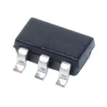
TINY SOT23-6 PACKAGE
D
D
D
D OPERATION TO 150°C
D POWER-SUPPLY TEMPERATURE
D
D
D
D
D
NOTEBOOK COMPUTERS
CELL PHONES
BATTERY MANAGEMENT
OFFICE MACHINES
The TMP121 and TMP123 are SPI-compatible temperature sensors available in the tiny SOT23-6 package.
Requiring no external components, the TMP121 and
TMP123 are capable of measuring temperatures within
2°C of accuracy over a temperature range of −40°C to
+125°C. Low supply current, and a supply range from 2.7V
to 5.5V, make the TMP121 and TMP123 excellent
candidates for low-power applications.
The TMP121 and TMP123 are ideal for extended thermal
measurement in a variety of communication, computer,
consumer, environmental, industrial, and instrumentation
applications.
APPLICATIONS
MONITORING
COMPUTER PERIPHERAL THERMAL
PROTECTION
DESCRIPTION
Temperature
Temperature
NC
1
Diode
Temp.
Sensor
Control
Logic
6
SO
GND
1
Diode
Temp.
Sensor
Control
Logic
6
SO
GND
2
∆Σ
A/D
Converter
Serial
Interface
5
CS
NC
2
∆Σ
A/D
Converter
Serial
Interface
5
CS
V+
3
OSC
Config.
and Temp.
Register
4
SCK
V+
3
OSC
Config.
and Temp.
Register
4
SCK
TMP121
TMP123
NC = No Connection(1)
NC = No Connection(1)
(1) Pins labeled NC should be left floating or connected to GND.
Please be aware that an important notice concerning availability, standard warranty, and use in critical applications of Texas Instruments
semiconductor products and disclaimers thereto appears at the end of this data sheet.
All trademarks are the property of their respective owners.
Copyright 2003−2005, Texas Instruments Incorporated
��������� �
�
��
�������� �� ������� �� �
����������� ����� ��������
���
��� �� �����
�������� ��� ��� ����� �
����� ����������� �������� ���������
���������� ���������! ���� ��� ����������� ������� ������! �
��� �����������
www.ti.com
��"�#$#
�"�#$%
www.ti.com
SBOS273C − JUNE 2003 − REVISED FEBRUARY 2005
ABSOLUTE MAXIMUM RATINGS(1)
Power Supply, V+ . . . . . . . . . . . . . . . . . . . . . . . . . . . . . . . . . . . . . . 7V
Input Voltage(2) . . . . . . . . . . . . . . . . . . . . . . . . . . . . . . . −0.3V to +7V
Input Current . . . . . . . . . . . . . . . . . . . . . . . . . . . . . . . . . . . . . . . 10mA
Operating Temperature Range . . . . . . . . . . . . . . . −55°C to +150°C
Storage Temperature Range . . . . . . . . . . . . . . . . . −60°C to +150°C
Junction Temperature (TJ max) . . . . . . . . . . . . . . . . . . . . . . +150°C
Lead Temperature (soldering) . . . . . . . . . . . . . . . . . . . . . . . . +300°C
(1) Stresses above these ratings may cause permanent damage.
Exposure to absolute maximum conditions for extended periods
may degrade device reliability. These are stress ratings only, and
functional operation of the device at these or any other conditions
beyond those specified is not supported.
(2) Input voltage rating applies to all TMP121 and TMP123 input
This integrated circuit can be damaged by ESD. Texas
Instruments recommends that all integrated circuits be
handled with appropriate precautions. Failure to observe
proper handling and installation procedures can cause damage.
ESD damage can range from subtle performance degradation to
complete device failure. Precision integrated circuits may be more
susceptible to damage because very small parametric changes could
cause the device not to meet its published specifications.
voltages.
ORDERING INFORMATION(1)
PRODUCT
PACKAGE-LEAD
PACKAGE DESIGNATOR
SOT23-6
DBV
TMP121
PACKAGE MARKING
T121
TMP123
T123
(1) For the most current package and ordering information, see the Package Option Addendum at the end of this document, or see the TI web site
at www.ti.com.
PIN CONFIGURATIONS
Top View
SOT23-6
TMP121(1)
GND
2
V+
3
6
SO
GND
1
5
CS
NC
2
4
SCK
V+
3
SOT23−6
NC = No Connection(2)
2
6
SO
5
CS
4
SCK
SOT23−6
NC = No Connection(2)
Pin 1 orientation is determined by package marking.
(1) Pin 1 of the SOT23-6 package is determined by orienting the package marking as shown.
(2) Pins labeled NC should be left floating or connected to GND.
T123
1
T121
NC
TMP123(1)
��"�#$#
�"�#$%
www.ti.com
SBOS273C − JUNE 2003 − REVISED FEBRUARY 2005
ELECTRICAL CHARACTERISTICS
At TA = −40°C to +125°C and V+ = 2.7V to 5.5V, unless otherwise noted.
TMP121, TMP123
PARAMETER
CONDITIONS
MIN
TYP
MAX
UNIT
TEMPERATURE INPUT
+125
°C
−25°C to +85°C
±0.5
±1.5
°C
−40°C to +125°C
±1.0
±2.0
°C
−40°C to +150°C
±1.5
+0.3
°C/V
Range
−40
Accuracy (temperature error)
vs Supply
−0.3
0.1
°C
±0.0625
Resolution
°C
DIGITAL INPUT/OUTPUT
Input Logic Levels:
VIH
VIL
Input Current, SO, SCK, CS
0.7(V+)
IIN
V
0V ≤ VIN ≤ V+
0.3(V+)
V
±1
µA
0.4
V
Output Logic Levels:
VOL SO
VOH SO
ISINK = 3mA
ISOURCE = 2mA
(V+)−0.4
V
Resolution
12
Input Capacitance, SO, SCK, CS
2.5
Bits
pF
Conversion Time
12-Bit
240
320
ms
Conversion Period(1)
12-Bit
480
640
ms
POWER SUPPLY
Operating Range
Quiescent Current
Shutdown Current (TMP121)
Shutdown Current (TMP123)
5.5
V
IQ
Serial Bus Inactive
2.7
35
50
µA
ISD
ISD
Serial Bus Inactive
0.1
1
µA
Serial Bus Inactive
0.1
3
µA
TEMPERATURE RANGE
Specified Range
−40
+125
°C
Operating Range
−55
+150
°C
Storage Range
−60
+150
Thermal Resistance
qJA
SOT23-6 Surface-Mount
200
°C
°C/W
(1) Period indicates time between conversion starts.
3
��"�#$#
�"�#$%
www.ti.com
SBOS273C − JUNE 2003 − REVISED FEBRUARY 2005
TYPICAL CHARACTERISTICS
At TA = +25°C and V+ = 5.0V, unless otherwise noted.
SHUTDOWN CURRENT vs TEMPERATURE
QUIESCENT CURRENT vs TEMPERATURE
1.0
50
0.9
V+ = 5V
0.8
40
0.7
30
V+ = 2.7V
ISD (µA)
IQ (µA)
0.6
0.5
0.4
0.3
0.2
20
0.1
0.0
Serial Bus Inactive
−0.1
−60 −40 −20
10
−60 −40 −20
0
20
40
60
80
100
120 140
0
20
40
60
80
100
120 140
Temperature (_ C)
Temperature (_ C)
CONVERSION TIME vs TEMPERATURE
TEMPERATURE ACCURACY vs TEMPERATURE
400
2.0
300
Temperature Error (_C)
Conversion Time (ms)
1.5
V+ = 5V
200
V+ = 2.7V
1.0
0.5
0.0
−0.5
−1.0
−1.5
12−Bit Resolution
100
−60 −40 −20
0
20
40
60
Temperature (_ C)
4
80
100
120 140
3 Typical Units 12−Bit Resolution
−2.0
−60 −40 −20 0
20 40 60
80 100 120 140 160
Temperature (_ C)
��"�#$#
�"�#$%
www.ti.com
SBOS273C − JUNE 2003 − REVISED FEBRUARY 2005
APPLICATIONS INFORMATION
The TMP121 and TMP123 are 12-bit plus sign read-only
digital temperature sensors optimal for thermal
management and thermal protection applications. The
TMP121 and the TMP123 communicate through a serial
interface that is SPI-compatible. Temperature is converted
to a 12-bit plus sign data word with 0.0625°C resolution.
The TMP121 and TMP123 are specified for a temperature
range of −40°C to +125°C, with operation extending from
−55°C to +150°C.
The TMP121 and TMP123 are optimal for low power
applications, with a 0.5s conversion period for reduced
power consumption. The TMP121 and TMP123 are
specified for a supply voltage range of 2.7V to 5.5V, and
also feature a hardware shutdown to provide additional
power savings.
The TMP121 and TMP123 require no external
components for operation, though a 0.1µF supply bypass
capacitor is recommended. Figure 1 shows typical
connections for the TMP121 and TMP123.
V+
V+
0.1µF
0.1µF
3
SCK
4
SO
6
3
1
NC(1)
TMP121
5
SCK
4
SO
6
2
5
D15
D14
D13
D12
D11
D10
D9
D8
T12
T11
T10
T9
T8
T7
T6
T5
D7
D6
D5
D4
D3
D2
D1
D0
T4
T3
T2
T1
T0
0
Z
Z
Table 1. Temperature Register
TEMPERATURE
(°C)
DIGITAL OUTPUT(1)
(BINARY)
HEX
150
0100 1011 0000 0000
4B00
125
0011 1110 1000 0000
3E80
25
0000 1100 1000 0000
0C80
0.0625
0000 0000 0000 1000
0008
0
0000 0000 0000 0000
0000
−0.0625
1111 1111 1111 1000
FFF8
−25
1111 0011 1000 0000
F380
−55
1110 0100 1000 0000
E480
CS
1
NC = No Connection
GND
The Temperature Register of the TMP121 and TMP123 is
a 16-bit, signed read-only register that stores the output of
the most recent conversion. Up to 16 bits can be read to
obtain data and are described in Table 1. The first 13 bits
are used to indicate temperature with bits D2 = 0, and D1,
D0 in a high impedance state. Data format for temperature
is summarized in Table 2. Following power-up or reset, the
Temperature Register will read 0°C until the first
conversion is complete.
(1) The last two bits are high impedance and are shown as 00 in the
table.
TMP123
CS
2
NC(1)
TEMPERATURE REGISTER
Table 2. Temperature Data Format
COMMUNICATING WITH THE TMP121
GND
NOTE: (1) Pins labeled NC should be left floating or connected to GND.
Figure 1. Typical Connections of the TMP121 and
TMP123
The sensing device of both the TMP121 and TMP123 is
the chip itself; the die flag of the lead frame is thermally
connected to pin 2 of the TMP121, and of the TMP123.
Thermal paths run through the package leads as well as
the plastic package, and the lower thermal resistance of
metal causes the leads to provide the primary thermal
path. The GND pin (pin 2) of the TMP121 and the NC pin
(pin 2) of the TMP123 are thermally connected to the metal
lead frame, and are the best choice for thermal input.
To maintain accuracy in applications requiring air or
surface temperature measurement, care should be taken
to isolate the package and leads from ambient air
temperature.
The TMP121 and TMP123 continuously convert
temperatures to digital data while CS is high. CS must be
high for a minimum of one conversion time (320ms max)
to update the temperature data. Reading temperature data
from the TMP121 and TMP123 is initiated by pulling CS
low, which will cause any conversion in progress to
terminate, and place the device into analog shutdown.
Quiescent current is reduced to 1µA during analog
shutdown. Once CS is pulled low, temperature data from
the last completed conversion prior to dropping CS is
latched into the shift register and clocked out at SO on the
falling SCK edge. The 16-bit data word is clocked out sign
bit first, followed by the MSB. Any portion of the 16-bit word
can be read before raising CS. The TMP121 and TMP123
typically require 0.25s to complete a conversion and
consume 50µA of current during this period. If CS is held
high for longer than one conversion time period the
TMP121 and TMP123 will go into idle mode for 0.25s,
requiring only 20µA of current. A new conversion begins
every 0.5s. Figure 2 describes the conversion timing for
the TMP121 and TMP123.
5
��"�#$#
�"�#$%
www.ti.com
SBOS273C − JUNE 2003 − REVISED FEBRUARY 2005
Timing Diagrams
0.5s
0.25s
The TMP121 and TMP123 are SPI-compatible. Figure 4
and Figure 5 describe the various timing requirements,
with parameters defined in Table 3.
50µA (active)
20µA (idle)
PARAMETER
Figure 2. Conversion Time and Period
MIN
SCK Period
t1
t2
100
40
CS to Output Data Delay
t3
t4
CS Rising Edge to Output High Impedance
t5
SCK Falling Edge to Output Data Delay
The serial data of the TMP121 and TMP123 consists of
12-bit plus sign temperature data followed by a
confirmation bit and two high impedance bits. Data is
transmitted in Binary Two’s Complement format. Figure 3
describes the output data of the TMP121 and TMP123.
CS to Rising Edge SCK Set-Up Time
D15
D14
D13
D12
D11
D10
D9
Table 3. Timing Description
D8
D7
D6
D5
D4
D3
1
Z
Z
Figure 3. Data READ
SCK
t3
t1
t2
CS
t4
SO
Figure 4. Output Data Timing Diagram
SCK
SCK
CS
CS
t5
t5
SO
SO
Figure 5. High Impedance Output Timing Diagram
6
ns
ns
SCK
Z
UNITS
ns
30
CS
SO/I
MAX
30
ns
30
ns
�PACKAGE OPTION ADDENDUM
www.ti.com
18-Sep-2008
PACKAGING INFORMATION
Orderable Device
Status (1)
Package
Type
Package
Drawing
Pins Package Eco Plan (2)
Qty
TMP121AIDBVR
ACTIVE
SOT-23
DBV
6
3000 Green (RoHS &
no Sb/Br)
CU NIPDAU
Level-2-260C-1 YEAR
TMP121AIDBVRG4
ACTIVE
SOT-23
DBV
6
3000 Green (RoHS &
no Sb/Br)
CU NIPDAU
Level-2-260C-1 YEAR
TMP121AIDBVT
ACTIVE
SOT-23
DBV
6
250
Green (RoHS &
no Sb/Br)
CU NIPDAU
Level-2-260C-1 YEAR
TMP121AIDBVTG4
ACTIVE
SOT-23
DBV
6
250
Green (RoHS &
no Sb/Br)
CU NIPDAU
Level-2-260C-1 YEAR
TMP123AIDBVR
ACTIVE
SOT-23
DBV
6
3000 Green (RoHS &
no Sb/Br)
CU NIPDAU
Level-2-260C-1 YEAR
TMP123AIDBVRG4
ACTIVE
SOT-23
DBV
6
3000 Green (RoHS &
no Sb/Br)
CU NIPDAU
Level-2-260C-1 YEAR
TMP123AIDBVT
ACTIVE
SOT-23
DBV
6
250
Green (RoHS &
no Sb/Br)
CU NIPDAU
Level-2-260C-1 YEAR
TMP123AIDBVTG4
ACTIVE
SOT-23
DBV
6
250
Green (RoHS &
no Sb/Br)
CU NIPDAU
Level-2-260C-1 YEAR
Lead/Ball Finish
MSL Peak Temp (3)
(1)
The marketing status values are defined as follows:
ACTIVE: Product device recommended for new designs.
LIFEBUY: TI has announced that the device will be discontinued, and a lifetime-buy period is in effect.
NRND: Not recommended for new designs. Device is in production to support existing customers, but TI does not recommend using this part in
a new design.
PREVIEW: Device has been announced but is not in production. Samples may or may not be available.
OBSOLETE: TI has discontinued the production of the device.
(2)
Eco Plan - The planned eco-friendly classification: Pb-Free (RoHS), Pb-Free (RoHS Exempt), or Green (RoHS & no Sb/Br) - please check
http://www.ti.com/productcontent for the latest availability information and additional product content details.
TBD: The Pb-Free/Green conversion plan has not been defined.
Pb-Free (RoHS): TI's terms "Lead-Free" or "Pb-Free" mean semiconductor products that are compatible with the current RoHS requirements
for all 6 substances, including the requirement that lead not exceed 0.1% by weight in homogeneous materials. Where designed to be soldered
at high temperatures, TI Pb-Free products are suitable for use in specified lead-free processes.
Pb-Free (RoHS Exempt): This component has a RoHS exemption for either 1) lead-based flip-chip solder bumps used between the die and
package, or 2) lead-based die adhesive used between the die and leadframe. The component is otherwise considered Pb-Free (RoHS
compatible) as defined above.
Green (RoHS & no Sb/Br): TI defines "Green" to mean Pb-Free (RoHS compatible), and free of Bromine (Br) and Antimony (Sb) based flame
retardants (Br or Sb do not exceed 0.1% by weight in homogeneous material)
(3)
MSL, Peak Temp. -- The Moisture Sensitivity Level rating according to the JEDEC industry standard classifications, and peak solder
temperature.
Important Information and Disclaimer:The information provided on this page represents TI's knowledge and belief as of the date that it is
provided. TI bases its knowledge and belief on information provided by third parties, and makes no representation or warranty as to the
accuracy of such information. Efforts are underway to better integrate information from third parties. TI has taken and continues to take
reasonable steps to provide representative and accurate information but may not have conducted destructive testing or chemical analysis on
incoming materials and chemicals. TI and TI suppliers consider certain information to be proprietary, and thus CAS numbers and other limited
information may not be available for release.
In no event shall TI's liability arising out of such information exceed the total purchase price of the TI part(s) at issue in this document sold by TI
to Customer on an annual basis.
OTHER QUALIFIED VERSIONS OF TMP121 :
• Enhanced Product: TMP121-EP
NOTE: Qualified Version Definitions:
Addendum-Page 1
�PACKAGE OPTION ADDENDUM
www.ti.com
18-Sep-2008
• Enhanced Product - Supports Defense, Aerospace and Medical Applications
Addendum-Page 2
�PACKAGE MATERIALS INFORMATION
www.ti.com
11-Mar-2008
TAPE AND REEL INFORMATION
*All dimensions are nominal
Device
Package Package Pins
Type Drawing
SPQ
Reel
Reel
Diameter Width
(mm) W1 (mm)
TMP121AIDBVR
SOT-23
DBV
6
3000
180.0
A0 (mm)
B0 (mm)
K0 (mm)
P1
(mm)
W
Pin1
(mm) Quadrant
8.4
3.2
3.1
1.39
4.0
8.0
Q3
TMP121AIDBVT
SOT-23
DBV
6
250
180.0
8.4
3.2
3.1
1.39
4.0
8.0
Q3
TMP123AIDBVR
SOT-23
DBV
6
3000
180.0
8.4
3.2
3.1
1.39
4.0
8.0
Q3
TMP123AIDBVT
SOT-23
DBV
6
250
180.0
8.4
3.2
3.1
1.39
4.0
8.0
Q3
Pack Materials-Page 1
�PACKAGE MATERIALS INFORMATION
www.ti.com
11-Mar-2008
*All dimensions are nominal
Device
Package Type
Package Drawing
Pins
SPQ
Length (mm)
Width (mm)
Height (mm)
TMP121AIDBVR
SOT-23
DBV
6
3000
190.5
212.7
31.8
TMP121AIDBVT
SOT-23
DBV
6
250
190.5
212.7
31.8
TMP123AIDBVR
SOT-23
DBV
6
3000
190.5
212.7
31.8
TMP123AIDBVT
SOT-23
DBV
6
250
190.5
212.7
31.8
Pack Materials-Page 2
��PACKAGE OPTION ADDENDUM
www.ti.com
14-Oct-2022
PACKAGING INFORMATION
Orderable Device
Status
(1)
Package Type Package Pins Package
Drawing
Qty
Eco Plan
(2)
Lead finish/
Ball material
MSL Peak Temp
Op Temp (°C)
Device Marking
(3)
Samples
(4/5)
(6)
TMP121AIDBVR
ACTIVE
SOT-23
DBV
6
3000
RoHS & Green
NIPDAU
Level-2-260C-1 YEAR
-40 to 125
T121
Samples
TMP121AIDBVRG4
ACTIVE
SOT-23
DBV
6
3000
RoHS & Green
NIPDAU
Level-2-260C-1 YEAR
-40 to 125
T121
Samples
TMP121AIDBVT
ACTIVE
SOT-23
DBV
6
250
RoHS & Green
NIPDAU
Level-2-260C-1 YEAR
-40 to 125
T121
Samples
TMP121AIDBVTG4
ACTIVE
SOT-23
DBV
6
250
RoHS & Green
NIPDAU
Level-2-260C-1 YEAR
-40 to 125
T121
Samples
TMP123AIDBVR
ACTIVE
SOT-23
DBV
6
3000
RoHS & Green
NIPDAU
Level-2-260C-1 YEAR
-55 to 125
T123
Samples
TMP123AIDBVT
ACTIVE
SOT-23
DBV
6
250
RoHS & Green
NIPDAU
Level-2-260C-1 YEAR
-55 to 125
T123
Samples
TMP123AIDBVTG4
ACTIVE
SOT-23
DBV
6
250
RoHS & Green
NIPDAU
Level-2-260C-1 YEAR
-55 to 125
T123
Samples
(1)
The marketing status values are defined as follows:
ACTIVE: Product device recommended for new designs.
LIFEBUY: TI has announced that the device will be discontinued, and a lifetime-buy period is in effect.
NRND: Not recommended for new designs. Device is in production to support existing customers, but TI does not recommend using this part in a new design.
PREVIEW: Device has been announced but is not in production. Samples may or may not be available.
OBSOLETE: TI has discontinued the production of the device.
(2)
RoHS: TI defines "RoHS" to mean semiconductor products that are compliant with the current EU RoHS requirements for all 10 RoHS substances, including the requirement that RoHS substance
do not exceed 0.1% by weight in homogeneous materials. Where designed to be soldered at high temperatures, "RoHS" products are suitable for use in specified lead-free processes. TI may
reference these types of products as "Pb-Free".
RoHS Exempt: TI defines "RoHS Exempt" to mean products that contain lead but are compliant with EU RoHS pursuant to a specific EU RoHS exemption.
Green: TI defines "Green" to mean the content of Chlorine (Cl) and Bromine (Br) based flame retardants meet JS709B low halogen requirements of