TMP144
TMP144
SBOS891B – OCTOBER 2018 – REVISED APRIL
2021
SBOS891B – OCTOBER 2018 – REVISED APRIL 2021
www.ti.com
TMP144 Low-Power, Digital Temperature Sensor With SMAART Wire™ / UART
Interface
1 Features
3 Description
•
The TMP144 digital output temperature sensor can
read temperatures to a resolution of 0.0625 °C.
•
•
•
•
•
•
•
•
Multiple Device Access (MDA):
– Global read/write operations
SMAART Wire™ / UART interface
Resolution: 12-bit or 0.0625 °C
±1 °C maximum (–10 °C to +100 °C)
±2 °C maximum (–40 °C to +125 °C)
Low quiescent current:
– 3-μA active IQ at 0.25 Hz
– 0.6-μA shutdown
Supply range: 1.4 V to 3.6 V
Push-pull digital output
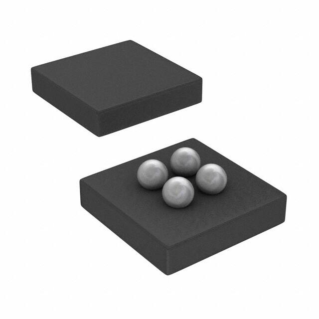
Package:
– 0.76 mm × 0.96 mm, 150-µm maximum height,
4-ball YMT (DSBGA)
– 0.76 mm × 0.96 mm, 625-µm maximum height,
4-ball YFF (DSBGA)
The device has a SMAART Wire™ / UART
interface that supports daisy-chain configurations. The
interface also supports Multiple Device Access (MDA)
commands that let the host communicate with multiple
devices on the bus simultaneously. MDA commands
are used as an alternative to sending individual
commands to each device on the bus. Up to 16
TMP144 devices can be attached together serially
and can be read by the host computer.
The TMP144 device is designed for spaceconstrained, power-sensitive applications with multiple
temperature measurement zones that must be
monitored. The device is specified for operation
over a temperature range of –40 °C to 125 °C
and is available in two different 4-ball, low-height
wafer chip-scale package (DSBGA) options. The YMT
package of the device has a height of 150 µm, which
is 40% thinner than a 0201 resistor. The thinner
YMT package can be placed under heat-dissipating
components on the system for better accuracy and
faster thermal response times.
2 Applications
•
•
•
•
•
•
•
•
Handsets
Smartphones
Tablets
LED Backlighting
HDTVs
Enterprise Servers
Notebooks
Medical
Device Information(1)
PART NUMBER
TMP144
(1)
VCC
TX
V
RX
+
TMP144
U1
GND
RX
0.76 mm x 0.96 mm
VCC
0.1µ F
0.1µ F
+
V
TX
YMT DSBGA (4)
VCC
0.1µ F
+
BODY SIZE (NOM)
0.76 mm x 0.96 mm
For all available packages, see the orderable addendum at
the end of the data sheet.
VCC
0.1µ F
Host
PACKAGE
YFF DSBGA (4)
+
V
TX
RX
TMP144
U2
V
TX
TMP144
U(n-1)
GND
GND
RX
TX
TMP144
U(n)
GND
RX
Up to 16 TMP144 devices can be configured as a daisy-chain. (See Device Nomenclature)
Simplified Application
An©IMPORTANT
NOTICEIncorporated
at the end of this data sheet addresses availability, warranty, changes, use in
safety-critical
applications,
Copyright
2021 Texas Instruments
Submit
Document
Feedback
intellectual property matters and other important disclaimers. PRODUCTION DATA.
Product Folder Links: TMP144
1
�TMP144
www.ti.com
SBOS891B – OCTOBER 2018 – REVISED APRIL 2021
Table of Contents
1 Features............................................................................1
2 Applications..................................................................... 1
3 Description.......................................................................1
4 Revision History.............................................................. 2
5 Pin Configuration and Functions...................................3
6 Specifications.................................................................. 4
6.1 Absolute Maximum Ratings ....................................... 4
6.2 ESD Ratings .............................................................. 4
6.3 Recommended Operating Conditions ........................4
6.4 Thermal Information ...................................................4
6.5 Electrical Characteristics ............................................4
6.6 UART Interface Timing ...............................................6
6.7 Timing Diagrams......................................................... 6
6.8 Typical Characteristics................................................ 7
7 Detailed Description........................................................8
7.1 Overview..................................................................... 8
7.2 Functional Block Diagram........................................... 8
7.3 Feature Description.....................................................9
7.4 Device Functional Modes..........................................10
7.5 SMAART Wire™ / UART Interface............................ 13
7.6 Register Maps...........................................................19
8 Application and Implementation.................................. 23
8.1 Application Information............................................. 23
8.2 Typical Application.................................................... 23
9 Power Supply Recommendations................................24
10 Layout...........................................................................25
10.1 Layout Guidelines................................................... 25
10.2 Layout Example...................................................... 25
11 Device and Documentation Support..........................26
11.1 Device Support........................................................26
11.2 Receiving Notification of Documentation Updates.. 26
11.3 Support Resources................................................. 26
11.4 Trademarks............................................................. 26
11.5 Electrostatic Discharge Caution.............................. 26
11.6 Glossary.................................................................. 26
12 Mechanical, Packaging, and Orderable
Information.................................................................... 26
4 Revision History
NOTE: Page numbers for previous revisions may differ from page numbers in the current version.
Changes from Revision A (February 2021) to Revision B (April 2021)
Page
• Removed Advanced Information note from YMT package................................................................................. 1
• Updated thermal information for YMT package.................................................................................................. 4
• Added typical value for pin capacitance............................................................................................................. 4
• Added active conversion current consumption limit values................................................................................ 4
• Added Figure 6-5 to the Typical Characteristics section.....................................................................................7
Changes from Revision * (October 2018) to Revision A (February 2021)
Page
• Changed data sheet status from Production Data to Production Mixed............................................................. 1
• Updated the numbering format for tables, figures, and cross-references throughout the document..................1
• Added Advanced Information YMT package...................................................................................................... 3
• Updated absolute max supply voltage from 3.6V to 4.0V...................................................................................4
• Updated TX pin absolute max from (V+) + 0.3 V to (V+) + 0.3 and ≤ 4 V.......................................................... 4
• Added digital temperature output section for result readout with different ETM mode setting........................... 9
• Updated the communication protocol description.............................................................................................13
• Added command byte value table.................................................................................................................... 13
• Added command flow for global software reset................................................................................................14
• Added command flow for global initialization and address assignment............................................................14
• Added command flow for global clear interrupt................................................................................................ 16
• Added command flow for global read and write................................................................................................16
• Added command flow for individual read and write.......................................................................................... 17
• Updated Register Map as per new format........................................................................................................ 19
• Updated temperature result register as a 16-bit value to map to the communication protocol.........................20
• Updated configuration register as a 16-bit value to map to the communication protocol................................. 20
• Updated temperature low limit register as a 16-bit value to map to the communication protocol.....................21
• Updated temperature high limit register as a 16-bit value to map to the communication protocol................... 22
2
Submit Document Feedback
Copyright © 2021 Texas Instruments Incorporated
Product Folder Links: TMP144
�TMP144
www.ti.com
SBOS891B – OCTOBER 2018 – REVISED APRIL 2021
5 Pin Configuration and Functions
B2
B2
B1
RX
TX
A2
A2
B1
RX
TX
A1
A1
V+
GND
V+
GND
No t to scale
No t to scale
Figure 5-2. YMT Package 4-Pin DSBGA (Top View)
Figure 5-1. YFF Package 4-Pin DSBGA (Top View)
Table 5-1. Pin Functions
PIN
(1)
NAME
NO.
GND
A2
RX
TX
V+
I/O(1)
DESCRIPTION
G
Ground
B2
I
Serial data input pin
B1
O
Serial data output pin (push-pull output)
A1
I
Supply voltage 1.4 V to 3.6 V
I = Input, O = Output, G = Ground
Submit Document Feedback
Copyright © 2021 Texas Instruments Incorporated
Product Folder Links: TMP144
3
�TMP144
www.ti.com
SBOS891B – OCTOBER 2018 – REVISED APRIL 2021
6 Specifications
6.1 Absolute Maximum Ratings
Over free-air temperature range unless otherwise noted(1)
MIN
Supply voltage
V+
Input voltage
RX
I/O current
TX
MAX
UNIT
–0.3
4.0
V
–0.3
(V+) + 0.3
and ≤ 4
V
±15
mA
Operating junction temperature, TJ
–55
150
°C
Storage temperature, Tstg
–60
150
°C
(1)
Stresses beyond those listed under Absolute Maximum Ratings may cause permanent damage to the device. These are stress
ratings only, which do not imply functional operation of the device at these or any other conditions beyond those indicated under
Recommended Operating Conditions. Exposure to absolute-maximum-rated conditions for extended periods may affect device
reliability.
6.2 ESD Ratings
V(ESD)
(1)
(2)
Electrostatic discharge
VALUE
UNIT
Human-body model (HBM), per ANSI/ESDA/JEDEC JS-001(1)
±2000
V
Charged-device model (CDM), per JEDEC specification JESD22-C101(2)
±1000
V
JEDEC document JEP155 states that 500-V HBM allows safe manufacturing with a standard ESD control process.
JEDEC document JEP157 states that 250-V CDM allows safe manufacturing with a standard ESD control process.
6.3 Recommended Operating Conditions
V+
Supply voltage
VI/O
RX
TA
Operating ambient temperature
MIN
NOM
MAX
1.4
3.3
3.6
UNIT
V
0
V+
V
-40
125
°C
6.4 Thermal Information
TMP144
THERMAL METRIC(1)
YFF (DSBGA)
YMT (DSBGA)
4 PINS
4 PINS
188.5
167.3
℃/W
UNIT
RθJA
Junction-to-ambient thermal resistance
RθJC(top)
Junction-to-case (top) thermal resistance
2.1
0.7
℃/W
RθJC(bot)
Junction-to-case (bottom) thermal resistance
NA
NA
℃/W
RθJB
Junction-to-board thermal resistance
35.1
47.0
℃/W
ψJT
Junction-to-top characterization parameter
10.6
0.4
℃/W
ψJB
Junction-to-board characterization parameter
35.1
47.0
℃/W
(1)
For more information about traditional and new thermal metrics, see the IC Package Thermal Metrics application report, SPRA953.
6.5 Electrical Characteristics
Over free-air temperature range and V+ = 1.4 V to 3.6 V (unless otherwise noted); Typical specifications are at TA = 25 °C
and V+ = 3.3 V (unless otherwise noted)
PARAMETER
TEST CONDITIONS
MIN
TYP
MAX
UNIT
TEMPERATURE SENSOR
TERR (1)
PSR
4
Temperature accuracy
V+ = 3.3 V, TA = –10 °C to 100 °C
±0.5
±1.0
°C
Temperature accuracy
V+ = 1.4 V to 3.6 V, TA = –40 °C to 125 °C
±1.0
±2.0
°C
DC power supply rejection
One-shot mode
±0.2
±0.5
°C/V
Submit Document Feedback
Copyright © 2021 Texas Instruments Incorporated
Product Folder Links: TMP144
�TMP144
www.ti.com
SBOS891B – OCTOBER 2018 – REVISED APRIL 2021
Over free-air temperature range and V+ = 1.4 V to 3.6 V (unless otherwise noted); Typical specifications are at TA = 25 °C
and V+ = 3.3 V (unless otherwise noted)
PARAMETER
TRES
Temperature resolution
tCONV
Conversion time
TEST CONDITIONS
MIN
Including sign bit
LSB
One-shot mode
MAX
UNIT
12
Bits
62.5
m°C
26
CR1 = 0, CR0 = 0 (default)
tCONV_P Conversion Period
TYP
35
ms
4
s
CR1 = 0, CR0 = 1
1
s
CR1 = 1, CR0 = 0
0.25
s
CR1 = 1, CR0 = 1
0.125
s
DIGITAL INPUT/OUTPUT
CIN
Input capacitance
VIH
Input logic high level
RX
0.7 × (V+)
5
(V+) + 0.3
–0.5
0.3 × (V+)
V
–1
1
μA
VIL
Input logic low level
RX
IIN
Input leakage current
0 ≤ VIN ≤ (V+) + 0.3V
VOL
Output low level
VOH
Output high level
pF
V
TX, V+ > 2V, IOH = 1 mA
0
0.4
V
TX, V+ < 2V, IOH = 1 mA
0
0.2 × (V+)
V
TX, V+ > 2V, IOL = 1 mA
(V+) – 0.4
V+
V
TX, V+ < 2V, IOL = 1 mA
0.8 × (V+)
V+
V
μA
POWER SUPPLY
IDD_ACTI Supply current during active
conversion
VE
V+ = 3.3V, Active Conversion, serial bus inactive
44
100
IDD_AVG Average current consumption
V+ = 3.3V, CR1 = 0, CR0 Serial bus inactive
= 0 (default)
Serial bus active
3
10
53
μA
IDD_SB
Standby current(2)
V+ = 3.3V, Serial bus inactive
2.5
9.5
μA
IDD_SD
Shutdown current
V+ = 3.3V, Serial bus inactive
0.6
5
μA
VPOR
Power-on reset threshold
voltage
Supply rising
0.9
VDD ramp time requirements
Supply rising or falling
tRAMP_V
DD
(1)
(2)
V
1
ms
Does not include effects of self heating.
Quiescent current between conversions
Submit Document Feedback
Copyright © 2021 Texas Instruments Incorporated
Product Folder Links: TMP144
5
�TMP144
www.ti.com
SBOS891B – OCTOBER 2018 – REVISED APRIL 2021
6.6 UART Interface Timing
Over free-air temperature range and V+ = 1.4 V to 3.6 V (unless otherwise noted)
UART (8N1)
MIN
Baud Rate
4.8
MAX
UNIT
114
kbps
tR
Data rise time
0.5%
Baud
tF
Data fall time
0.5%
Baud
±1
Baud
Jitter
6.7 Timing Diagrams
BaudTYP
Jitter -
tR
tF
Jitter +
Figure 6-1. SMAART Wire™ / UART Interface Timing Diagram
6
Submit Document Feedback
Copyright © 2021 Texas Instruments Incorporated
Product Folder Links: TMP144
�TMP144
www.ti.com
SBOS891B – OCTOBER 2018 – REVISED APRIL 2021
6.8 Typical Characteristics
12
9
V+ = 1.4 V
V+ = 1.8 V
V+ = 3.6 V
10
7
8
6
ISD (mA)
IQ (mA)
V+ = 1.8 V
V+ = 3.6 V
8
6
5
4
3
4
2
2
1
0
0
-60 -40 -20
0
20
40
60
80
-60 -40 -20
100 120 140 160
0
40
60
80
100 120 140 160
Temperature (°C)
Temperature (°C)
Figure 6-3. Shutdown Current vs. Temperature
Figure 6-2. Typical Quiescent Current vs. Temperature
27.5
1
V+ = 1.4 V
V+ = 1.8 V
V+ = 3.6 V
27
26.5
26
25.5
25
24.5
V+ = 3.3 V
V+ = 1.8 V
0.8
0.6
Temperature Error (qC)
Conversion Time (ms)
20
0.4
0.2
0
-0.2
-0.4
-0.6
24
-0.8
23.5
-60 -40 -20
0
20
40
60
80
100 120 140 160
Temperature (°C)
Figure 6-4. Conversion Time vs. Temperature
-1
-40
-15
10
35
60
Temperature (qC)
85
110 125
TMP1
Figure 6-5. Temperature Error vs. Temperature (YFF Package)
Submit Document Feedback
Copyright © 2021 Texas Instruments Incorporated
Product Folder Links: TMP144
7
�TMP144
www.ti.com
SBOS891B – OCTOBER 2018 – REVISED APRIL 2021
7 Detailed Description
7.1 Overview
The TMP144 is a digital output temperature sensor in a wafer chip-scale package (WCSP) that is designed for
thermal management and thermal profiling. The TMP144 includes a SMAART Wire™ / UART interface that can
communicate in a daisy-chain loop with up to 16 devices on a single bus. The interface requires two pins from
the host: the first device in the daisy-chain receives data from the host and the last device in the daisy-chain
returns data to the host, closing the loop. In addition, the TMP144 can do multiple device access (MDA)
commands that allow multiple TMP144 devices to respond to a single global bus command. MDA commands
reduce communication time and power in a bus that contains multiple TMP144 devices. The operation of
TMP144, is specified over a temperature range of –40 °C to 125 °C.
The TMP144 can also configure the bus in a transparent mode, where the input from the host is sent directly
to the next device in the chain without delay. Additionally, the TMP144 can disconnect the chain and create a
serial communication controlled by each TMP144 on the bus, thereby allowing each device to have configurable
addressing and interrupt capabilities. The input pin, RX, is a high-impedance node. The output pin, TX, has an
internal push-pull output stage that can drive the host to GND or V+.
After an initialization sequence, each device on the bus is programmed with its own unique interface address
based upon its position in the chain, that allows it to respond to its own address. The devices can also respond
to general commands that permit the user to read or write to all devices on the bus without the need to send
individual addresses and commands to each device.
The temperature sensor in the TMP144 is the chip itself. Thermal paths run through the package bumps as
well as the package. The lower thermal resistance of metal and the low height of the devices, causes the
bumps and the topside to provide the dominant thermal paths to the sensing element on the device. To maintain
accuracy in applications that require air or surface temperature measurement, care should be taken to isolate
the package from ambient air temperature. A thermally-conductive adhesive can help to achieve accurate
surface temperature measurement.
7.2 Functional Block Diagram
V+
Rx
SW
Tx
Serial
Interface
Register
Bank
Oscillator
Control
Logic
Reset
Internal
Thermal
BJT
Temperature
Sensor
Circuitry
ADC
GND
8
Submit Document Feedback
Copyright © 2021 Texas Instruments Incorporated
Product Folder Links: TMP144
�TMP144
www.ti.com
SBOS891B – OCTOBER 2018 – REVISED APRIL 2021
7.3 Feature Description
7.3.1 Power Up
After power-up or general-call reset, the TMP144 immediately starts a conversion as shown in Figure 7-1. The
active conversion time (tACT) of the device is 26 ms (typical) and the first result is available after the conversion is
complete in the temperature result register.
tACT
tCONV
Start of
Conversion
Startup
Figure 7-1. Conversion Start
7.3.2 Digital Temperature Output
The TMP144 by default provides a 12-bit digital output for each temperature conversion, which is stored in
the temperature result register. The host application needs to read two bytes to obtain the data. Additionally,
the application may program the ETM bit in the configuration register to get a 13-bit digital output. Table 7-1
summarizes the temperature output format. One LSB equals 0.0625 °C resolution.
Table 7-1. Temperature Data Format
TEMPERATURE (°C)
DIGITAL OUTPUT (ETM = 0)
DIGITAL OUTPUT (ETM = 1)
BINARY (T11-T0)
HEX
BINARY (T12-T0)
HEX
+150
0111 1111 1111
7FF
0 1001 0110 0000
0960
+127.9375
0111 1111 1111
7FF
0 0111 1111 1111
07FF
+125
0111 1101 0000
7D0
0 0111 1101 0000
07D0
+100
0110 0100 0000
640
0 0110 0100 0000
0640
+80
0101 0000 0000
500
0 0101 0000 0000
0500
+75
0100 1011 0000
4B0
0 0100 1011 0000
04B0
+50
0011 0010 0000
320
0 0011 0010 0000
0320
+25
0001 1001 0000
190
0 0001 1001 0000
0190
+0.0625
0000 0000 0001
001
0 0000 0000 0001
0001
0
0000 0000 0000
000
0 0000 0000 0000
0000
-0.0625
1111 1111 1111
FFF
1 1111 1111 1111
1FFF
-25
1110 0111 0000
E70
1 1110 0111 0000
1E70
-40
1101 1000 0000
D80
1 1101 1000 0000
1D80
7.3.3 Timeout Function
A timeout mechanism is implemented on the TMP144 to allow for re-synchronization of the SMAART Wire™
interface if synchronization between the host and the TMP144 is lost for 28 ms (typical). If the timeout period
expires between the calibration byte and the command byte, between the command byte and a data byte, or
between any data bytes, the TMP144 resets the SMAART Wire™ interface circuitry and waits for the baud rate
calibration command to restart. Every time a byte is transmitted on the SMAART Wire™ interface, this timeout
period restarts.
Submit Document Feedback
Copyright © 2021 Texas Instruments Incorporated
Product Folder Links: TMP144
9
�TMP144
www.ti.com
SBOS891B – OCTOBER 2018 – REVISED APRIL 2021
7.4 Device Functional Modes
7.4.1 Continuous Conversion Mode
When the TMP144 is in Continuous Conversion mode (M1 = 1), continuous conversions are performed at a rate
determined by the conversion rate bits, CR[1:0], in the configuration register. The TMP144 performs a single
conversion, then powers down and waits for the appropriate delay set by CR[1:0].
7.4.2 Shutdown Mode
Shutdown mode saves maximum power by shutting down all device circuitry other than the serial interface,
reducing the current consumption to typically less than 0.5 μA. Shutdown mode is enabled when bits M[1:0] in
the configuration register are set as "00". If there is an active conversion ongoing, the device completes the
ongoing conversion, updates the temperature result register and shuts down.
7.4.3 One-Shot Mode
The TMP144 features a One-Shot Temperature Measurement mode. When the device is in Shutdown mode,
writing 01 to bits M[1:0] in the configuration register, starts a single temperature conversion. During the
conversion, the bits M[1:0] read 01. The device returns to the shutdown state at the completion of the single
conversion. After the conversion, bits M[1:0] read 00. This feature is useful for reducing power consumption in
the TMP144 when continuous temperature monitoring is not required.
As a result of the short conversion time, the TMP144 can achieve a higher conversion rate. A single conversion
typically takes 26 ms and an individual read can take place in less than 300 μs. When using One-Shot mode, 30
or more conversions per second are possible.
7.4.4 Extended Temperature Mode
At power on, the TMP144 operates with a 12-bit temperature output. However, the TMP144 can be programmed
to operate in Extended Temperature mode, by setting the ETM bit in the configuration register as '1'. When
operating in extended temperature mode, the temperature result and temperature limit registers will be 13-bit
instead of 12-bit. This extra bit increases the range of the measurement. As shown in Table 7-1, with a 12-bit
temperature, the maximum value is 7FFh or 127.9 °C. With a 13-bit temperature value, however, the maximum
value is FFFh or 255.9 °C.
When the extended temperature mode is enabled, the EM bit for the temperature high limit register and
temperature low limit registers is usable by the application. TI recommends that the user update the THIGH
and TLOW register limits because the added bit will effectively left shift and double the register value. This will
double the corresponding temperature limit. However, if the application exits the ETM mode, by changing the bit
from 1 to 0, this bit is not cleared. As a result, the limit will be right-shifted by 1 bit and halved unless the register
values are updated by the application.
The ETM bit value is considered at the end of every conversion cycle, but the limit registers can be updated
immediately after setting the bit to 1.
7.4.5 Temperature Alert Function
The TMP144 contains a temperature alert function that monitors the device temperature and compares the result
to the values stored in the temperature limit registers to determine if the device temperature is within these
set limits. As shown in Figure 7-2, if the result of the temperature conversion is greater than the value in the
temperature high limit register, the flag-high bit (FH) in the configuration register is set to '1'. If the result of the
temperature conversion register is less than the value in the temperature low limit register, the flag-low (FL) in
10
Submit Document Feedback
Copyright © 2021 Texas Instruments Incorporated
Product Folder Links: TMP144
�TMP144
www.ti.com
SBOS891B – OCTOBER 2018 – REVISED APRIL 2021
the configuration register is set to '1'. The clearing of the flag bits depends on the setting of the latch bit (LC) in
the configuration register.
THIGH
Measured
Temperature
TLOW
FH Bit
(Transparent Mode)
FL Bit
(Transparent Mode)
FH Bit
(Latch Mode)
FL Bit
(Latch Mode)
Time
Read of Configuration Register
Figure 7-2. Temperature Flag Functional Diagram
The LC bit in the configuration register when set to '1' is used to latch the value of the flag bits (FH and FL) until
the host issues a read command to the configuration register. The flag bits are set to '0' when a read command
is received by the device.
The LC bit when configured as '0', configures the device to operate in transparent mode, where the flag bits (FH
and FL) are cleared only when the result of the temperature conversion is within the temperature limits.
7.4.6 Interrupt Functionality
The TMP144 interrupts the host by disconnecting the bus and issuing an interrupt request by holding the bus low
if all of following conditions are met as shown in Figure 7-3.
•
•
•
INT_EN in the configuration register is set to 1;
The temperature result of the last conversion is greater than the value in the temperature high limit register or
less than the value in the temperature low limit register (also indicated by a 1 in either FH or FL, respectively);
The bus is logic high and idle for more than 28 ms.
Submit Document Feedback
Copyright © 2021 Texas Instruments Incorporated
Product Folder Links: TMP144
11
�TMP144
www.ti.com
SBOS891B – OCTOBER 2018 – REVISED APRIL 2021
RX
RX
Host
RX
TX
RX
TX
TX
TX
Interface Logic
Interface Logic
Interface Logic
Device(1)
Device(2)
Device(N)
Figure 7-3. TMP144 Daisy-Chain: Bus Status During an Interrupt Request (Logic Low) From Second
Device
The interrupt on the bus is latched regardless of the status of LC. Writing a 1 to INT_EN automatically sets the
LC bit. The TMP144 holds the bus low until one of the following events happen:
•
•
•
Global Interrupt Clear command is received.
Global Software Reset command is received.
A power-on reset event occurs.
Each of these events clears the INT_EN. The TMP144 does not issue future interrupts until the host writes sets
the INT_EN in the configuration register to re-enable future interrupts.
In a system with enabled interrupts, it is possible for a TMP144 on the bus to issue an interrupt at the same
time that the host starts a communication sequence. To avoid this scenario, TI recommends that the host should
check the status on the receiving side of the bus after transmitting the calibration byte. If it is 1, then the host can
continue with the communication. If it is 0, one of the TMP144 devices on the bus is issuing an alert and the host
must transmit a Global Interrupt Clear command.
12
Submit Document Feedback
Copyright © 2021 Texas Instruments Incorporated
Product Folder Links: TMP144
�TMP144
www.ti.com
SBOS891B – OCTOBER 2018 – REVISED APRIL 2021
7.5 SMAART Wire™ / UART Interface
The TMP144 uses a TI proprietary, one-wire UART-compatible communication protocol called SMAART Wire™.
The TMP144 has two dedicated pins for communication:TX and RX. Usually, these two pins are connected
internally and the signal on the RX propagates to the TX, unless the device must send data on the bus or during
address assignment and alert procedures.
The interface has built-in timeouts (typically 28 ms) that return the interface to a known state if communication is
disrupted.
7.5.1 Communication Protocol
Each communication of the SMAART Wire™ / UART protocol consists of 8-bit word, transferred least significant
bit (LSB) first. Each 8-bit word begins with a Start bit that is logic low, and ends with a Stop bit that is logic high.
By using a Start bit and Stop bit for each 8-bit word, the TMP144 can calibrate each word and keep synchronous
communication throughout the process.
The steps for the SMAART Wire™ / UART communication protocol are:
1. The host sends a Start bit to start the communication process.
2. The host sends the calibration byte (55h) to allow the TMP144 to sync to the baud rate of the host.
3. The host sends a Stop bit after the calibration byte.
4. The host sends a second Start bit, followed by the command register byte and a Stop bit.
5. The host sends a third Start bit, followed by the data byte only for writes.
6. The host will send the data byte(s) if the instruction is a write command.
7. The host sends a Stop bit to finish the process.
Note
The device will break the chain and send the data byte(s) if the instruction sent in the command
register is a read command.
The sequence is shown in Figure 7-4.
S
1
0
1
0
1
0
1
0
P
S
P
C0 C1 C2 C3 C4 C5 C6 C7
Calibration Byte (55h)
S D0 D1 D2 D3 D4 D5 D6 D7
Command with Address Pointer
P
S D8 D9 D10 D11D12 D13D14 D15 P
Register Data (8-bit)
Register Data (8-bit)
S = Start condition of SMAART Wire¡ protocol
P = Stop condition of SMAART Wire¡ protocol
Figure 7-4. Generic Communication Write Bitstream
Driven by TMP144
S
1
0
1
0
1
0
1
0
P
S
C0 C1 C2 C3 C4 C5 C6 C7
Calibration Byte (55h)
P
S D0 D1 D2 D3 D4 D5 D6 D7
Command with Address Pointer
P
S D8 D9 D10 D11D12 D13 D14 D15 P
Register Data (8-bit)
Register Data (8-bit)
1-bit default delay for
bus direction change
S = Start condition of SMAART Wire¡ protocol
P = Stop condition of SMAART Wire¡ protocol
Figure 7-5. Generic Communication Read Bitstream
The command byte is decoded by the TMP144 to determine the format of the subsequent communication
operation. Table 7-2 lists the command register byte values.
Table 7-2. Command Byte Value
COMMAND
OPERATION
COMMAND BYTE ENCODING
HEX VALUE
C7 (MSB)
C6
C5
C4
C3
C2
C1
C0 (LSB)
GLBL
IN3/ID3
IN2/ID2
IN1/ID1
IN0/ID0
P1
P0
R/W
Global software
reset
1
0
1
1
0
1
0
0
B4
Global
initialization
1
0
0
0
1
1
0
0
8C
Submit Document Feedback
Copyright © 2021 Texas Instruments Incorporated
Product Folder Links: TMP144
13
�TMP144
www.ti.com
SBOS891B – OCTOBER 2018 – REVISED APRIL 2021
Table 7-2. Command Byte Value (continued)
COMMAND
OPERATION
COMMAND BYTE ENCODING
HEX VALUE
C7 (MSB)
C6
C5
C4
C3
C2
C1
C0 (LSB)
GLBL
IN3/ID3
IN2/ID2
IN1/ID1
IN0/ID0
P1
P0
R/W
Global address
assignment
1
0
0
1
0
0
0
0
90
Global clear
interrupt
1
0
1
0
1
0
0
1
A9
Global write
1
1
1
1
0
P1
P0
0
Based on P[1:0]
Global read
1
1
1
1
0
P1
P0
1
Based on P[1:0]
Individual write
0
ID3
ID2
ID1
ID0
P1
P0
0
Based on ID[3:0] and
P[1:0]
Individual read
0
ID3
ID2
ID1
ID0
P1
P0
1
Based on ID[3:0] and
P[1:0]
7.5.2 Global Software Reset
The host can initiate a global software reset command (C[7:0] = 10110100) to all TMP144 devices in the
daisy-chain as shown in Figure 7-6. Upon receiving this command, the TMP144 resets all of its internal registers
except for the device ID and reconnects the bus. If the bus is broken before the initiation of this command,
all TMP144 devices before the broken bus point receive the command. If the host intends to initiate a global
software reset across all TMP144 devices in the chain, this command must be transmitted multiple times until it
echoes back to the host.
S
1
0
1
0
1
0
1
0
S
P
R/W
P0
P1
0
0
1
IN0/ID0 IN1/ID1 IN2/ID2 IN3/ID3
0
1
1
0
GLBL
1
P
Command Byte
Calibration Byte (55h)
Figure 7-6. Global Software Reset Command Flow
7.5.3 Global Initialization and Address Assignment Sequence
At device power-up, every TMP144 in the daisy-chain is connected in transparent mode, as shown in Figure 7-7.
RX
RX
Host
RX
TX
RX
TX
TX
TX
Interface Logic
Interface Logic
Interface Logic
Device(1)
Device(2)
Device(N)
Figure 7-7. TMP144 Daisy-Chain: Bus Status at Start of Global Initialization
14
Submit Document Feedback
Copyright © 2021 Texas Instruments Incorporated
Product Folder Links: TMP144
�TMP144
www.ti.com
SBOS891B – OCTOBER 2018 – REVISED APRIL 2021
As shown in Figure 7-8, the host must send the initialization command (C[7:0] = 10001100) for the bus to
program its internal address, depending on the number of devices on the bus.
Host TX
S
1
0
1
0
1
0
1
0
P
R/W
P0
P1
0
0
1
S
IN0/ID0 IN1/ID1 IN2/ID2 IN3/ID3
Calibration Byte (55h)
1
0
GLBL
0
0
1
P
Command Byte
Device-1
TX
S
1
0
1
0
1
0
1
0
P
S
0
0
1
1
0
0
0
1
P
Device-2
TX
S
1
0
1
0
1
0
1
0
P
S
0
0
1
1
0
0
0
1
P
S
1
0
0
0
1
0
0
1
P
Host TX
S
0
0
0
0
1
0
0
1
Devices
in Pass
Through
P
Address Assignment Command (90h)
Device-1
TX
Device 1 (TX) Device 2 (RX)
Device-2
TX
Host TX
Device-1
TX
Device-2
TX
S
0
1
0
0
1
0
0
1
P
Device 2 (TX) Device 3 (RX)
Figure 7-8. Global Initialization and Address Assignment Command Flow
Each TMP144 in the chain interprets the initialization command byte and disconnects the chain, as shown in
Figure 7-9.
RX
TX
RX
TX
RX
TX
RX
TX
Host
Interface Logic
Interface Logic
Interface Logic
Device(1)
Device(2)
Device(N)
Figure 7-9. TMP144 Daisy-Chain: Bus Status at Start of Address Assignment
The host must then send the address assignment command, consisting of C[7:4] = 1001 and C[3:0] = 0000,
where C[3:0] represents the address of the first device in the chain. This word is stored internally as its device
ID. The first device increments the unit in the device address and then reconnects the bus, as shown in Figure
7-10. This address is then sent to the next device in the chain.
Submit Document Feedback
Copyright © 2021 Texas Instruments Incorporated
Product Folder Links: TMP144
15
�TMP144
www.ti.com
SBOS891B – OCTOBER 2018 – REVISED APRIL 2021
RX
RX
RX
TX
Host
RX
TX
TX
TX
Interface Logic
Interface Logic
Interface Logic
Device(1)
Device(2)
Device(N)
Figure 7-10. TMP144 Daisy-Chain: Bus Status After First Device Address Assignment
After all devices on the chain have received the respective addresses, the host receives the last programmed
address on the chain + 1. The host can use this information to determine the total number of devices in the chain
and the respective address of each device.
After the initialization sequence, every device can be addressed individually or through global commands. This
global initialization sequence is a requirement and must be performed before any other communication.
7.5.4 Global Clear Interrupt
The host can initiate a global clear interrupt command (C[7:0] = 10101001) to all TMP144 devices in the
daisy-chain as shown in Figure 7-11. Upon receiving this command, the TMP144 disables future interrupts
(bit-11 in the Configuration Register is set to 0). If a TMP144 previously broke the bus connection and sent
an interrupt (logic low on the bus), the device now stops holding the bus low. The device sends the baud rate
calibration command and clear interrupt command to the next TMP144 in the chain, then reconnects the bus.
In the case of multiple devices having active interrupts, the clear interrupt command propagates through the
daisy-chain, disables all interrupts, and reconnects the bus across all devices.
0
1
S
1
1
0
0
1
0
R/W
P0
P1
1
0
0
S
P
IN0/ID0 IN1/ID1 IN2/ID2 IN3/ID3
0
1
1
0
GLBL
1
P
Command Byte
Calibration Byte (55h)
Figure 7-11. Global Clear Interrupt Command Flow
7.5.5 Global Read and Write
The host can initiate a global read or write command to all TMP144s in the daisy-chain by sending the read/write
command, consisting of C[7:3] = 11110 and C[2:1] to indicate the data register pointer P[1:0], as shown in Table
7-3. A global write command is indicated by C[0] = 0. The host must transfer at least one more byte of data for
the register, and every TMP144 in the daisy-chain updates the appropriate register as shown in Figure 7-12.
S
1
0
1
0
1
0
1
0
P
S
R/W
P0
P1
0
P0
P1
D0
D1
D2
D3
D4
0
1
GLBL
1
1
1
P
D13
D14
D15
P
Command Byte
Calibration Byte (55h)
S
IN0/ID0 IN1/ID1 IN2/ID2 IN3/ID3
D5
D6
D7
P
S
D8
D9
D10
D11
D12
Data Byte-2
Data Byte-1
Figure 7-12. Global Write Command Flow
16
Submit Document Feedback
Copyright © 2021 Texas Instruments Incorporated
Product Folder Links: TMP144
�TMP144
www.ti.com
SBOS891B – OCTOBER 2018 – REVISED APRIL 2021
A global read command is indicated by C[0] = 1. As shown in Figure 7-13, the TMP144 with the device ID of
0000 then breaks the bus connection, transmits the data from the register indicated by bits C[2:1] (corresponding
to data register pointer P[1:0]), and then reconnects the bus. The TMP144 with the device ID of 0001 then
repeats the same sequence, followed by the rest of the TMP144 devices in the daisy-chain.
0
1
S
Host TX
1
0
0
1
1
0
S
P
R/W
P0
P1
IN0/ID0 IN1/ID1 IN2/ID2 IN3/ID3
1
P0
P1
0
0
1
S
1
0
1
1
1
P
P
Command Byte
Calibration Byte (55h)
Host RX
1
GLBL
0
1
1
0
S
P
1
P1
P0
0
1
1
1
1
D11
D12
D13
D14
D15
Devices
in Pass
Through
Host TX
S
Host RX
D0
D1
D2
D4
D3
D5
D6
D7
D9
D8
S
P
D10
Device-1 Data Byte-1
P
Device-1 Data Byte-2
Host TX
D0
S
Host RX
D1
D2
D3
D5
D4
D6
D7
P
D8
S
D10
D9
D12
D11
D13
D14
D15
P
Device-2 Data Byte-2
Device-2 Data Byte-1
Figure 7-13. Global Read Command Flow
Table 7-3. Pointer Addresses
P1
P0
REGISTER
0
0
Temperature register (read-only)
0
1
Configuration register (read/write)
1
0
TLOW register (read/write)
1
1
THIGH register (read/write)
7.5.6 Individual Read and Write
The host can initiate an individual read and write command to a particular TMP144 device in the daisy-chain by
sending the read/write command. The read/write command consists of these parameters:
•
•
•
•
C[7] = 0 (Individual device access)
C[6:3] = the device ID (ID[3:0])
C[2:1] = the data register pointer (P[1:0]); see Table 7-3
C[0] = indicates read/write control
As shown in Figure 7-14, an individual device write command is indicated by C[0] = 0. The host must transfer
at least one more byte of data for the register indicated by bits C[2:1]. The TMP144 in the daisy-chain that
corresponds to the device ID noted by bits C[6:3] then updates the appropriate register.
S
1
0
1
1
0
0
1
0
P
S
R/W
P0
P1
0
P0
P1
D0
D1
D2
D3
D4
ID0
ID1
GLBL
ID2
ID3
0
P
D13
D14
D15
P
Command Byte
Calibration Byte (55h)
S
IN0/ID0 IN1/ID1 IN2/ID2 IN3/ID3
D5
D6
D7
P
S
D8
Host Data Byte-1
D9
D10
D11
D12
Host Data Byte-2
Figure 7-14. Individual Write Command Flow
Submit Document Feedback
Copyright © 2021 Texas Instruments Incorporated
Product Folder Links: TMP144
17
�TMP144
www.ti.com
SBOS891B – OCTOBER 2018 – REVISED APRIL 2021
As shown in Figure 7-15, an individual device read command is indicated by C[0] = 1. As shown in Figure 7-16,
the TMP144 in the daisy-chain that corresponds to the device ID pointed by bits C[6:3] then breaks the bus,
transmits the data from the register pointed by bits C[2:1], and reconnects the bus.
S
Host TX
1
0
1
0
1
0
1
0
P
S
R/W
P0
P1
1
P0
P1
ID1
ID0
GLBL
ID2
ID3
0
P
Command Byte
Calibration Byte (55h)
Host RX
IN0/ID0 IN1/ID1 IN2/ID2 IN3/ID3
S
1
0
1
0
1
0
1
0
P
S
1
P0
P1
ID0
ID1
ID2
ID3
0
P
S
D0
D1
D2
D3
D4
D5
D6
D7
P
S
D8
D9
D10
D11
D12
D13
D14
D15
P
Devices
in Pass
Through
Host TX
Host RX
Device-1 Data Byte-1
Device-1 Data Byte-2
Figure 7-15. Individual Read Command Flow
RX
TX
RX
TX
RX
TX
RX
TX
Host
Interface Logic
Interface Logic
Interface Logic
Device(1)
Device(2)
Device(N)
Figure 7-16. TMP144 Daisy-Chain: Bus Status During Individual Read Operation of Second Device
18
Submit Document Feedback
Copyright © 2021 Texas Instruments Incorporated
Product Folder Links: TMP144
�TMP144
www.ti.com
SBOS891B – OCTOBER 2018 – REVISED APRIL 2021
7.6 Register Maps
Figure 7-17 shows the internal register structure of the TMP144. Communications between the registers are
transferred through the interface in LSB-first order. The 8-bit command register as shown in , is used to
determine the address pointer for the register that the host device wants to access.
Command
Register
Temperature
Register
Configuration
Register
RX
I/O
Control
Interface
Temperature Low
Limit Register
TX
Temperature High
Limit Register
Figure 7-17. Internal Register Structure
Table 7-4. Register Map
ADDRESS
POINTER P[1:0]
TYPE
RESET
ACRONYM
REGISTER NAME
SECTION
00
R
0000h
Temp_Result
Temperature result register
Go
01
R/W
0200h
Configuration
Configuration Register
Go
10
R/W
3C00h
Tlow_limit
Temperature low limit register
Go
11
R/W
F600h
Thigh_limit
Temperature high limit register
Go
Table 7-5. Register Section/Block Access Type Codes
Access Type
Code
Description
R
R
Read
RC
R
Read
C
to Clear
R
Read
-0
Returns 0s
W
W
Write
W0CP
W
W
0C
0 to clear
P
Requires privileged access
Read Type
R-0
Write Type
Reset or Default Value
-n
Value after reset or the default value
Submit Document Feedback
Copyright © 2021 Texas Instruments Incorporated
Product Folder Links: TMP144
19
�TMP144
www.ti.com
SBOS891B – OCTOBER 2018 – REVISED APRIL 2021
7.6.1 Temperature Result Register (P[1:0] = 00) [reset = 0000h]
The temperature result register stores the results of the conversion in 12-bit or 13-bit format, depending on the
state of the ETM bit in the configuration register. Negative numbers are represented in two's complement format.
Following power-up or reset the temperature result register reads 0 °C, until the first conversion is complete.
When the ETM bit is configured as '0', the temperature result register of the device is configured as 12-bit value
with the least significant bit always reading '0'. One LSB for the temperature result equals 0.0625 °C.
Table 7-6. Temperature Result Register (ETM = 0)
15
14
13
12
11
10
9
8
7
6
5
4
3
2
1
T[11:0]
EM
Reserved
R-000h
R-0
R-0h
0
Table 7-7. Temperature Result Register (ETM = 0) Field Description
Bit
15:4
3
2:0
Field
Type
Reset
Description
T[11:0]
R
000h
12-bit temperature result after last conversion
EM
R
0
Extended mode bit
Reserved
R
0h
Reserved
When the ETM bit is configured as '1', the temperature result register of the device is configured as 13-bit value.
One LSB for the temperature result equals 0.0625 °C.
Table 7-8. Temperature Result Register (ETM = 1)
15
14
13
12
11
10
9
8
7
6
5
4
3
2
1
T[12:0]
Reserved
R-0000h
R-0h
0
Table 7-9. Temperature Result Register (ETM = 1) Field Description
Bit
15:13
2:0
Field
Type
Reset
Description
T[12:0]
R
0000h
13-bit temperature result after last conversion
Reserved
R
0h
Reserved
7.6.2 Configuration Register (P[1:0] = 01) [reset = 0200h]
The configuration register is used to store bits that control the operational modes of the temperature sensors and
read the status of alert flags. Read/write operations are performed LSB first.
Return to Register Map.
Table 7-10. Configuration Register
15
14
13
12
11
10
9
8
7
6
5
4
3
INT_E
N
CR[1:0]
FH
FL
LC
M[1:0]
ETM
Reserved
R/W-0
R/W-0
R-0
R-0
R/W-0
R/W-10
R/W-0
R-00h
2
1
0
Table 7-11. Configuration Register Field Description
20
Bit
Field
Type
Reset
Description
15
INT_EN
R/W
0
Interrupt enable bit
0 = Interrupt is disabled
1 = Interrupt is enabled
14:13
CR[1:0]
R/W
0
Conversion rate select
00 = 0.25 Hz conversion rate (default)
01 = 1 Hz conversion rate
10 = 4 Hz conversion rate
11 = 8 Hz conversion rate
Submit Document Feedback
Copyright © 2021 Texas Instruments Incorporated
Product Folder Links: TMP144
�TMP144
www.ti.com
SBOS891B – OCTOBER 2018 – REVISED APRIL 2021
Table 7-11. Configuration Register Field Description (continued)
Bit
Field
Type
Reset
Description
12
FH
R
0
Flag high temperature
0 = High temperature limit not crossed
1 = High temperature limit crossed
11
FL
R
0
Flag low temperature
0 = Low temperature limit not crossed
1 = Low temperature limit crossed
10
LC
R/W
0
Latch control bit
0 = Flag bits are cleared on read
1 = Flag bits are latched
9:8
M[1:0]
R/W
10
Conversion mode select
00 = Shutdown mode
01 = One shot conversion mode
1x = Continuous conversion mode
ETM
R/W
0
Extended temperature mode select
0 = Mode is disabled
1 = Mode is enabled
Reserved
R
0
Reserved
7
6:0
7.6.3 Temperature Low Limit Register (P[1:0] = 10) [reset = F600h]
The temperature low limit register is used to store the low temperature threshold for the device low limit flag. The
default power up reset value is -10 °C. The power on default value is valid only when ETM = 0. At the end of
each temperature conversion, the device compares the temperature result with the temperature low limit register.
If the temperature result is less than the threshold set in this register, the FL bit in the configuration register is
set.
When the ETM bit in the configuration register is updated, it is strongly recommended that the user update the
low limit register.
Note
When the ETM bit is set to 0, any writes to the EM bit will be ignored.
Table 7-12. Temperature Low Limit Register (ETM = 0)
15
14
13
12
11
10
9
8
7
6
5
4
3
2
1
L[11:0]
EM
Reserved
R/W-F60h
R/W-0
R-0h
0
Table 7-13. Temperature Low Limit Register (ETM = 0) Field Description
Bit
15:4
3
2:0
Field
Type
Reset
Description
L[11:0]
R/W
F60h
12-bit temperature low limit threshold
EM
R/W
0
Don't care when ETM = 0
Reserved
R
0h
Reserved
Table 7-14. Temperature Low Limit Register (ETM = 1)
15
14
13
12
11
10
9
8
7
6
5
4
3
2
1
L[12:0]
Reserved
R/W-F600h
R-0h
0
Table 7-15. Temperature Low Limit Register (ETM = 1) Field Description
Bit
Field
Type
Reset
Description
15:3
L[12:0]
R/W
F600h
13-bit temperature low limit threshold
2:0
Reserved
R
0h
Reserved
Submit Document Feedback
Copyright © 2021 Texas Instruments Incorporated
Product Folder Links: TMP144
21
�TMP144
www.ti.com
SBOS891B – OCTOBER 2018 – REVISED APRIL 2021
7.6.4 Temperature High Limit Register (P[1:0] = 11) [reset = 3C00h]
The temperature high limit register is used to store the high temperature threshold for the device high limit flag.
The default power up reset value is +60 °C. The power on default value is valid only when ETM = 0. At the
end of each temperature conversion, the device compares the temperature result with the temperature high limit
register. If the temperature result is greater than the threshold set in this register, the FH bit in the configuration
register is set.
When the ETM bit in the configuration register is updated, it is strongly recommended that the user update the
high limit register.
Note
When the ETM bit is set to 0, any writes to the EM bit will be ignored.
Table 7-16. Temperature High Limit Register (ETM = 0)
15
14
13
12
11
10
9
8
7
6
5
4
3
2
1
H[11:0]
EM
Reserved
R/W-3C0h
R/W-0
R-0h
0
Table 7-17. Temperature High Limit Register (ETM = 0) Field Description
Bit
15:4
3
2:0
Field
Type
Reset
Description
H[11:1]
R/W
3C0h
12-bit temperature high limit threshold
EM
R/W
0
Don't care when ETM = 0
Reserved
R
0h
Reserved
Table 7-18. Temperature High Limit Register (ETM = 1)
15
14
13
12
11
10
9
8
7
6
5
4
3
2
1
H[12:0]
Reserved
R/W-3C00h
R-0h
0
Table 7-19. Temperature High Limit Register (ETM = 1) Field Description
Bit
22
Field
Type
Reset
Description
15:3
H[12:0]
R/W
3C00h
13-bit temperature high limit threshold
2:0
Reserved
R
0h
Reserved
Submit Document Feedback
Copyright © 2021 Texas Instruments Incorporated
Product Folder Links: TMP144
�TMP144
www.ti.com
SBOS891B – OCTOBER 2018 – REVISED APRIL 2021
8 Application and Implementation
Note
Information in the following applications sections is not part of the TI component specification,
and TI does not warrant its accuracy or completeness. TI’s customers are responsible for
determining suitability of components for their purposes, as well as validating and testing their design
implementation to confirm system functionality.
8.1 Application Information
The TMP144 devices are typically used to for thermal management of multiple hotspots. The MDA commands
make it easy to manage multiple devices at the same time, which reduces communication time and power. The
WCSP package enables the device to be placed in space-constrained designs and allows the device to have a
fast thermal response.
8.2 Typical Application
Figure 8-1 shows typical connections for TMP144 devices in a daisy-chain configuration.
Figure 8-1. Typical Application With Multiple Devices
8.2.1 Design Requirements
Multiple devices are connected in this typical application. The key design requirements are discussed in the
following sections.
8.2.2 Detailed Design Procedure
8.2.2.1 Trace Length
The maximum trace or cable length between two TMP144 devices can vary because of the effective resistance
and capacitance of the type of cable used in a customer application. Design the trace or cable such that timing
specifications in Timing Diagrams can be satisfied for each TMP144 device in the daisy-chain.
8.2.2.2 Voltage Drop Effect
Take into account the voltage drop that occurs along the supply and ground lines as a result of the currents of
all the devices on the line. This voltage drop occurs as a result of multiple devices simultaneously consuming
current through the combined resistance of the common wire, connectors, and solder contacts. Make sure that
the supply on the last device does not fall below the minimum operating supply of 1.4 V.
Submit Document Feedback
Copyright © 2021 Texas Instruments Incorporated
Product Folder Links: TMP144
23
�TMP144
www.ti.com
SBOS891B – OCTOBER 2018 – REVISED APRIL 2021
8.2.2.3 Power Supply Noise Filtering
To reduce power supply noise, a 0.1-μF bypass capacitor is used for each TMP144 device. Depending on the
environment, additional bypass capacitors (for example, 1 nF) may be required.
8.2.3 Application Curves
12
10
3
V+ = 1.4 V
V+ = 1.8 V
V+ = 3.6 V
2.5
2
1.5
Temperature Error (qC)
IQ (mA)
8
6
4
2
1
0.5
0
-0.5
-1
-1.5
0
-60 -40 -20
0
20
40
60
80
-2
100 120 140 160
-2.5
Temperature (°C)
-3
-60
-40
-20
0
20
40
60
80
100
120
140
Temperature (qC)
Figure 8-2. Typical Quiescent Current vs.
Temperature
Figure 8-3. Temperature Error vs. Temperature
9 Power Supply Recommendations
The TMP144 operates on a power-supply range from 1.4 V to 3.6 V. The device is trimmed for operation at a
3.3-V supply, but the TMP144 can measure temperature accurately in the full supply range.
The TMP144 is a very low-power device and generates very low noise on the supply bus. Applying a bypass
capacitor to the V+ pin of the TMP144 can further reduce any noise the TMP144 might propagate to other
components. Use a CF capacitor with a value greater than 0.1 μF as shown in Figure 9-1. Place the bypass
capacitor as close to the supply and ground pins of the device as possible for best results.
VCC
CF
• 0.1 PF
+
V
RX
TX
GND
Figure 9-1. Power Supply Noise Reduction With a Bypass Capacitor
24
Submit Document Feedback
Copyright © 2021 Texas Instruments Incorporated
Product Folder Links: TMP144
�TMP144
www.ti.com
SBOS891B – OCTOBER 2018 – REVISED APRIL 2021
10 Layout
10.1 Layout Guidelines
Mount the TMP144 to a PCB as shown in Figure 10-1. Obtaining acceptable performance with alternate layout
schemes is possible, however this layout produces good results and is intended as a guideline:
•
•
•
•
Bypass the V+ pin to ground with a low-ESR ceramic bypass-capacitor. The typical recommended bypass
capacitance is a 0.1-μF ceramic capacitor with a X5R or X7R dielectric. The optimum placement is closest
to the V+ and GND pins of the device. Take care to minimize the loop area formed by the bypass-capacitor
connection, the V+ pin, and the GND pin of the IC. Alternatively, the bypass capacitor can also be grounded
through a via connected to the GND plane.
Use larger copper area pads to reduce self-heating and lower thermal resistance to the environment.
If possible, use PCB boards with thick copper layers.
If possible, do not use stain to protect the IC because stain can increase thermal resistance.
10.2 Layout Example
VIA to power plane
VIA to ground plane
B2/
RX
B1/
TX
A2/
GND
A1/
V+
0.1µ F
Figure 10-1. Layout Example
Submit Document Feedback
Copyright © 2021 Texas Instruments Incorporated
Product Folder Links: TMP144
25
�TMP144
www.ti.com
SBOS891B – OCTOBER 2018 – REVISED APRIL 2021
11 Device and Documentation Support
11.1 Device Support
11.1.1 Device Nomenclature
daisychain
A method of propagating signals along a bus in which the devices are connected in series and the
signal passed from one device to the next. The daisy-chain scheme permits assignment of device
priorities based on the electrical position of the device on the bus.
11.2 Receiving Notification of Documentation Updates
To receive notification of documentation updates, navigate to the device product folder on ti.com. In the upper
right corner, click on Alert me to register and receive a weekly digest of any product information that has
changed. For change details, review the revision history included in any revised document.
11.3 Support Resources
TI E2E™ support forums are an engineer's go-to source for fast, verified answers and design help — straight
from the experts. Search existing answers or ask your own question to get the quick design help you need.
Linked content is provided "AS IS" by the respective contributors. They do not constitute TI specifications and do
not necessarily reflect TI's views; see TI's Terms of Use.
11.4 Trademarks
SMAART Wire™ and TI E2E™ are trademarks of Texas Instruments.
All trademarks are the property of their respective owners.
11.5 Electrostatic Discharge Caution
This integrated circuit can be damaged by ESD. Texas Instruments recommends that all integrated circuits be handled
with appropriate precautions. Failure to observe proper handling and installation procedures can cause damage.
ESD damage can range from subtle performance degradation to complete device failure. Precision integrated circuits may
be more susceptible to damage because very small parametric changes could cause the device not to meet its published
specifications.
11.6 Glossary
TI Glossary
This glossary lists and explains terms, acronyms, and definitions.
12 Mechanical, Packaging, and Orderable Information
The following pages include mechanical, packaging, and orderable information. This information is the most
current data available for the designated devices. This data is subject to change without notice and revision of
this document. For browser-based versions of this data sheet, refer to the left-hand navigation.
26
Submit Document Feedback
Copyright © 2021 Texas Instruments Incorporated
Product Folder Links: TMP144
�TMP144
www.ti.com
SBOS891B – OCTOBER 2018 – REVISED APRIL 2021
PACKAGE OUTLINE
YMT0004
PicoStar TM - 0.15 mm max height
SCALE 20.000
PicoStar
B
E
0.4 TYP
A
2
1
PIN A1
CORNER
A
0.2 TYP
D
SYMM
0.4
TYP
B
0.15 MAX
4X
0.015
0.26
0.20
C A B
SYMM
C
SEATING PLANE
0.018
0.008
4225388/B 08/2020
PicoStar is a trademark of Texas Instruments.
NOTES:
1. All linear dimensions are in millimeters. Any dimensions in parenthesis are for reference only. Dimensioning and tolerancing
per ASME Y14.5M.
2. This drawing is subject to change without notice.
www.ti.com
Submit Document Feedback
Copyright © 2021 Texas Instruments Incorporated
Product Folder Links: TMP144
27
�TMP144
www.ti.com
SBOS891B – OCTOBER 2018 – REVISED APRIL 2021
EXAMPLE BOARD LAYOUT
YMT0004
PicoStar TM - 0.15 mm max height
PicoStar
(0.4) TYP
4X (
2
1
0.23)
A
(0.2) TYP
SYMM
B
SYMM
LAND PATTERN EXAMPLE
EXPOSED METAL SHOWN
SCALE:60X
( 0.23)
METAL
SOLDER MASK
OPENING
0.05 MAX
EXPOSED
METAL
0.05 MIN
METAL UNDER
SOLDER MASK
EXPOSED
METAL
( 0.23)
SOLDER MASK
OPENING
NON-SOLDER MASK
DEFINED
(PREFERRED)
SOLDER MASK
DEFINED
SOLDER MASK DETAILS
NOT TO SCALE
4225388/B 08/2020
NOTES: (continued)
3. Final dimensions may vary due to manufacturing tolerance considerations and also routing constraints.
For more information, see Texas Instruments literature number SLUA271 (www.ti.com/lit/slua271).
www.ti.com
28
Submit Document Feedback
Copyright © 2021 Texas Instruments Incorporated
Product Folder Links: TMP144
�TMP144
www.ti.com
SBOS891B – OCTOBER 2018 – REVISED APRIL 2021
EXAMPLE STENCIL DESIGN
YMT0004
PicoStar TM - 0.15 mm max height
PicoStar
(0.4) TYP
2
1
4X ( 0.21)
A
(0.2) TYP
SYMM
METAL
TYP
B
(R0.05) TYP
SYMM
SOLDER PASTE EXAMPLE
BASED ON 0.075 mm THICK STENCIL
SCALE:60X
4225388/B 08/2020
NOTES: (continued)
4. Laser cutting apertures with trapezoidal walls and rounded corners may offer better paste release.
www.ti.com
Submit Document Feedback
Copyright © 2021 Texas Instruments Incorporated
Product Folder Links: TMP144
29
�PACKAGE OPTION ADDENDUM
www.ti.com
22-Apr-2021
PACKAGING INFORMATION
Orderable Device
Status
(1)
Package Type Package Pins Package
Drawing
Qty
Eco Plan
(2)
Lead finish/
Ball material
MSL Peak Temp
Op Temp (°C)
Device Marking
(3)
(4/5)
(6)
TMP144YFFR
ACTIVE
DSBGA
YFF
4
3000
RoHS & Green
SNAGCU
Level-1-260C-UNLIM
-40 to 125
C2
TMP144YFFT
ACTIVE
DSBGA
YFF
4
250
RoHS & Green
SNAGCU
Level-1-260C-UNLIM
-40 to 125
C2
TMP144YMTR
ACTIVE
PICOSTAR
YMT
4
3000
RoHS & Green
Call TI
Level-1-260C-UNLIM
-40 to 125
TMP144YMTT
ACTIVE
PICOSTAR
YMT
4
250
RoHS & Green
Call TI
Level-1-260C-UNLIM
-40 to 125
(1)
The marketing status values are defined as follows:
ACTIVE: Product device recommended for new designs.
LIFEBUY: TI has announced that the device will be discontinued, and a lifetime-buy period is in effect.
NRND: Not recommended for new designs. Device is in production to support existing customers, but TI does not recommend using this part in a new design.
PREVIEW: Device has been announced but is not in production. Samples may or may not be available.
OBSOLETE: TI has discontinued the production of the device.
(2)
RoHS: TI defines "RoHS" to mean semiconductor products that are compliant with the current EU RoHS requirements for all 10 RoHS substances, including the requirement that RoHS substance
do not exceed 0.1% by weight in homogeneous materials. Where designed to be soldered at high temperatures, "RoHS" products are suitable for use in specified lead-free processes. TI may
reference these types of products as "Pb-Free".
RoHS Exempt: TI defines "RoHS Exempt" to mean products that contain lead but are compliant with EU RoHS pursuant to a specific EU RoHS exemption.
Green: TI defines "Green" to mean the content of Chlorine (Cl) and Bromine (Br) based flame retardants meet JS709B low halogen requirements of