Order
Now
Product
Folder
Support &
Community
Tools &
Software
Technical
Documents
TMP464
SBOS835C – MAY 2017 – REVISED OCTOBER 2019
TMP464 High-Accuracy 5-Channel (4-Remote and 1-Local) Temperature Sensor
1 Features
3 Description
•
•
•
•
•
The TMP464 device is a high-accuracy, low-power
temperature sensor using a two-wire, SMBus or I2C
compatible interface. Up to four remote diodeconnected temperature zones can be monitored
simultaneously in addition to the local temperature.
Aggregating the temperature measurements across a
system allows improved performance through tighter
guard bands and can reduce board complexity. A
typical use case is for monitoring the temperature
across different processors, such as MCUs, GPUs,
and FPGAs in complex systems such as servers and
telecommunications equipment. Advanced features
such as series resistance cancellation, programmable
non-ideality factor, programmable offset, and
programmable temperature limits are included to
provide a robust thermal monitoring solution with
improved accuracy and noise immunity.
1
•
•
•
•
•
4-Channel Remote Diode Temperature Sensor
Local and Remote Accuracy: ±0.75°C (Maximum)
Temperature Resolution: 0.0625°C
Supply and Logic Voltage Range: 1.7 V to 3.6 V
43-µA Operating Current (1 SPS, All Channels
Active)
0.3-µA Shutdown Current
Remote Diode: Series Resistance Cancellation,
η-Factor Correction, Offset Correction, and Diode
Fault Detection
Register Lock Function Secures Key Registers
I2C or SMBus™ Compatible Two-Wire Interface
With Pin-Programmable Address
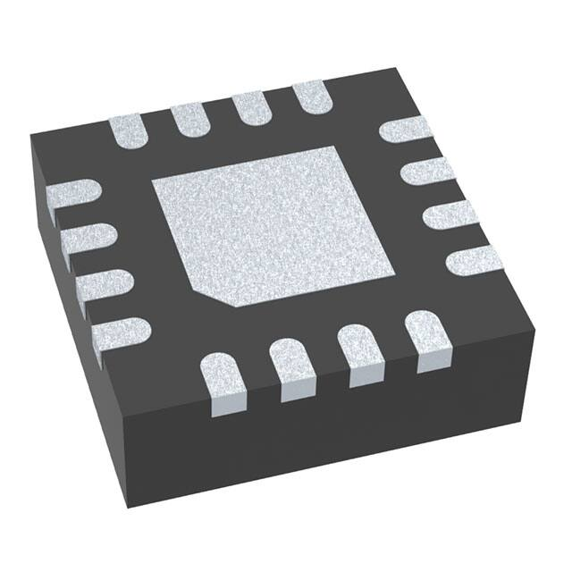
16-pin VQFN Package
Each of the four remote channels (and the local
channel) can be programmed independently with two
thresholds that are triggered when the corresponding
temperature is exceeded at the measured location. In
addition, there is a programmable hysteresis setting
to avoid constant toggling around the threshold.
2 Applications
•
•
•
•
•
•
•
•
MCU, GPU, ASIC, FPGA, DSP, and CPU
Temperature Monitoring
Telecommunication Equipment
Servers and Personal Computers
Cloud Ethernet Switches
Secure Data Centers
Highly Integrated Medical Systems
Precision Instruments and Test Equipment
LED Lighting Thermal Control
The TMP464 device provides high accuracy (0.75°C)
and high resolution (0.0625°C) measurement
capabilities. The device supports low voltage rails
(1.7 V to 3.6 V), common two-wire interfaces, and is
available in a small, space efficient package (3 mm ×
3 mm) for easy integration into computing systems.
The remote junction supports a temperature range
from –55°C to +150°C. The TMP464 has a
preprogrammed temperature limit of 125°C.
Device Information(1)
PART NUMBER
TMP464
PACKAGE
VQFN (16)
BODY SIZE (NOM)
3.00 mm × 3.00 mm
(1) For all available packages, see the orderable addendum at
the end of the data sheet.
Typical Application Schematic
Remote
Remote
Remote
Zone 4
Zone 3
Zone 2
Remote
1.7 V to 3.6 V
Zone 1
CBYPASS
RS1
RS2
CDIFF
RS1
RS2
CDIFF
RS1
RS2
CDIFF
RS1
RS2
RSCL RSDA RT2 RT
14
V+
CDIFF
6
5
4
3
7
13
D1+
TMP464 SCL
D2+
D3+
SDA
D4+
D-
THERM2
12
2-Wire Interface
SMBus / I2C
Compatible
Controller
11
10
THERM
Local
9
ADD
Overtemperature
Shutdown
Zone 5
GND
8
Copyright © 2017, Texas Instruments Incorporated
See the Design Requirements section for remote diode recommendations.
1
An IMPORTANT NOTICE at the end of this data sheet addresses availability, warranty, changes, use in safety-critical applications,
intellectual property matters and other important disclaimers. PRODUCTION DATA.
�TMP464
SBOS835C – MAY 2017 – REVISED OCTOBER 2019
www.ti.com
Table of Contents
1
2
3
4
5
6
7
Features ..................................................................
Applications ...........................................................
Description .............................................................
Revision History.....................................................
Pin Configuration and Functions .........................
Specifications.........................................................
1
1
1
2
3
4
6.1
6.2
6.3
6.4
6.5
6.6
6.7
4
4
4
4
5
6
7
Absolute Maximum Ratings ......................................
ESD Ratings..............................................................
Recommended Operating Conditions.......................
Thermal Information ..................................................
Electrical Characteristics...........................................
Two-Wire Timing Requirements ...............................
Typical Characteristics ..............................................
Detailed Description .............................................. 9
7.1 Overview ................................................................... 9
7.2 Functional Block Diagram ......................................... 9
7.3 Feature Description................................................. 10
7.4 Device Functional Modes........................................ 12
7.5 Programming........................................................... 12
7.6 Register Maps ......................................................... 18
8
Application and Implementation ........................ 28
8.1 Application Information............................................ 28
8.2 Typical Application .................................................. 28
9 Power Supply Recommendations...................... 31
10 Layout................................................................... 32
10.1 Layout Guidelines ................................................. 32
10.2 Layout Example .................................................... 33
11 Device and Documentation Support ................. 34
11.1
11.2
11.3
11.4
11.5
Receiving Notification of Documentation Updates
Community Resources..........................................
Trademarks ...........................................................
Electrostatic Discharge Caution ............................
Glossary ................................................................
34
34
34
34
34
12 Mechanical, Packaging, and Orderable
Information ........................................................... 34
4 Revision History
NOTE: Page numbers for previous revisions may differ from page numbers in the current version.
Changes from Revision B (August 2017) to Revision C
•
Changed the Device ID code from: 0x0464 to: 0x1468 ...................................................................................................... 27
Changes from Revision A (June 2017) to Revision B
•
2
Page
Changed 'QFN' to 'VQFN' in table header as per industry standard ..................................................................................... 4
Changes from Original (May 2017) to Revision A
•
Page
Page
Updated packaging information ........................................................................................................................................... 34
Submit Documentation Feedback
Copyright © 2017–2019, Texas Instruments Incorporated
Product Folder Links: TMP464
�TMP464
www.ti.com
SBOS835C – MAY 2017 – REVISED OCTOBER 2019
5 Pin Configuration and Functions
NC
1
NC
2
NC
NC
V+
SCL
16
15
14
13
TMP464 RGT Package
16-Pin VQFN With Exposed Thermal Pad
Top View
12
SDA
11
THERM2
THERM
Thermal Pad
7
8
GND
9
D±
4
6
D3+
D1+
10
5
3
D2+
D4+
ADD
Not to scale
NC - No internal connection
Pin Functions
PIN
NAME
NO.
TYPE
DESCRIPTION
ADD
9
Digital Input
Address select. Connect to GND, V+, SDA, or SCL.
D1+
6
Analog input
Positive connection to remote temperature sensors. A total of 4 remote channels are
supported. An unused channel must be connected to D–.
D2+
5
Analog input
Positive connection to remote temperature sensors. A total of 4 remote channels are
supported. An unused channel must be connected to D–.
D3+
4
Analog input
Positive connection to remote temperature sensors. A total of 4 remote channels are
supported. An unused channel must be connected to D–.
D4+
3
Analog input
Positive connection to remote temperature sensors. A total of 4 remote channels are
supported. An unused channel must be connected to D–.
D–
7
Analog input
Negative connection to remote temperature sensors. Common for 4 remote channels.
GND
8
Ground
NC
1, 2, 15, 16
—
SCL
13
Digital input
SDA
12
THERM
10
Digital output
Thermal shutdown or fan-control pin.
Active low; open-drain; requires a pullup resistor to a voltage between 1.7 V and 3.6 V, not
necessarily V+. If this pin is not used it may be left open or grounded.
THERM2
11
Digital output
Second THERM output.
Active low; open-drain; requires a pullup resistor to a voltage between 1.7 V and 3.6 V, not
necessarily V+. If this pin is not used it may be left open or grounded.
V+
14
Power supply
Positive supply voltage, 1.7 V to 3.6 V; requires 0.1-µF bypass capacitor to ground.
Supply ground connection
No connection, may be left floating or connected to GND or V+
Serial clock line for I2C or SMBus compatible two-wire interface.
Input; requires a pullup resistor to a voltage between 1.7 V and 3.6 V (not necessarily V+) if
driven by an open-drain output.
Bidirectional digital Serial data line for I2C- or SMBus compatible two-wire interface. Open-drain; requires a pullup
input-output
resistor to a voltage between 1.7 V and 3.6 V, not necessarily V+.
Submit Documentation Feedback
Copyright © 2017–2019, Texas Instruments Incorporated
Product Folder Links: TMP464
3
�TMP464
SBOS835C – MAY 2017 – REVISED OCTOBER 2019
www.ti.com
6 Specifications
6.1 Absolute Maximum Ratings
over operating free-air temperature range (unless otherwise noted) (1)
Power supply
Input voltage
Input current
MIN
MAX
UNIT
V+
–0.3
6
V
THERM, THERM2, SDA, SCL, and ADD only
–0.3
6
D1+ through D4+
–0.3
((V+) + 0.3)
and ≤ 6
D– only
–0.3
0.3
SDA sink
–25
All other pins
–10
10
–55
150
°C
150
°C
150
°C
Operating temperature
Junction temperature (TJ, maximum)
Storage temperature, Tstg
(1)
–60
V
mA
Stresses beyond those listed under Absolute Maximum Ratings may cause permanent damage to the device. These are stress ratings
only, which do not imply functional operation of the device at these or any other conditions beyond those indicated under Recommended
Operating Conditions. Exposure to absolute-maximum-rated conditions for extended periods may affect device reliability.
6.2 ESD Ratings
VALUE
V(ESD)
(1)
(2)
Electrostatic discharge
Human body model (HBM), per ANSI/ESDA/JEDEC JS-001 (1)
±2000
Charged device model (CDM), JEDEC specification JESD22-C101 (2)
±750
UNIT
V
JEDEC document JEP155 states that 500-V HBM allows safe manufacturing with a standard ESD control process.
JEDEC document JEP157 states that 250-V CDM allows safe manufacturing with a standard ESD control process.
6.3 Recommended Operating Conditions
over operating free-air temperature range (unless otherwise noted)
MIN
NOM
MAX
UNIT
V+
Supply voltage
1.7
3.6
V
TA
Operating free-air temperature
–40
125
°C
TD
Remote junction temperature
–55
150
°C
6.4 Thermal Information
TMP464
THERMAL METRIC
RGT (VQFN)
UNIT
16 PINS
RθJA
Junction-to-ambient thermal resistance
46
°C/W
RθJC(top)
Junction-to-case (top) thermal resistance
43
°C/W
RθJB
Junction-to-board thermal resistance
17
°C/W
ψJT
Junction-to-top characterization parameter
0.8
°C/W
ψJB
Junction-to-board characterization parameter
5
°C/W
4
Submit Documentation Feedback
Copyright © 2017–2019, Texas Instruments Incorporated
Product Folder Links: TMP464
�TMP464
www.ti.com
SBOS835C – MAY 2017 – REVISED OCTOBER 2019
6.5 Electrical Characteristics
at TA = –40°C to +125°C and V+ = 1.7 V to 3.6 V (unless otherwise noted)
PARAMETER
TEST CONDITIONS
MIN
TYP
MAX
UNIT
TA = –40°C to 100°C, V+ = 1.7 V to 3.6 V
–0.75
±0.125
0.75
°C
TA = –40°C to 125°C, V+ = 1.7 V to 3.6 V
–1
±0.5
1
°C
TA = –10°C to 85°C, TD = –55°C to 150°C
V+ = 1.7 V to 3.6 V
–0.75
±0.125
0.75
–1
±0.5
1
TEMPERATURE MEASUREMENT
TLOCAL
TREMOTE
Local temperature sensor accuracy
Remote temperature sensor accuracy
TA = –40°C to 125°C, TD = –55°C to 150°C
V+ = 1.7 V to 3.6 V
Local temperature error supply sensitivity
V+ = 1.7 V to 3.6 V
–0.15
±0.05
0.15
°C/V
Remote temperature error supply sensitivity
V+ = 1.7 V to 3.6 V
–0.25
±0.1
0.25
°C/V
Temperature resolution
(local and remote)
ADC conversion time
0.0625
One-shot mode, per channel (local or remote)
16
ADC resolution
°C
17
13
High
Remote sensor
source current
Medium
ms
Bits
120
Series resistance 1 kΩ (maximum)
45
Low
η
°C
µA
7.5
Remote transistor ideality factor
1.008
SERIAL INTERFACE (SCL, SDA)
VIH
High-level input voltage
VIL
Low-level input voltage
0.7 × (V+)
Hysteresis
200
SDA output-low sink current
VOL
Low-level output voltage
Serial bus input leakage current
V
0.3 × (V+)
20
IO = –20 mA, V+ ≥ 2 V
mA
0.15
IO = –15 mA, V+ < 2 V
0 V ≤ VIN ≤ 3.6 V
–1
Serial bus input capacitance
V
mV
0.4
V
0.2 × V+
V
1
μA
4
pF
DIGITAL INPUTS (ADD)
VIH
High-level input voltage
VIL
Low-level input voltage
Input leakage current
0.7 × (V+)
0 V ≤ VIN ≤ 3.6 V
V
–0.3
0.3 × (V+)
V
–1
1
μA
Input capacitance
4
pF
DIGITAL OUTPUTS (THERM, THERM2)
Output-low sink current
VOL = 0.4 V
VOL
Low-level output voltage
IO = –6 mA
IOH
High-level output leakage current
VO = V+
6
mA
0.15
0.4
V
1
μA
3.6
V
POWER SUPPLY
V+
IQ
Specified supply voltage range
Quiescent current
POR
Power-on-reset threshold
POH
Power-on-reset hysteresis
1.7
Active conversion, local sensor
240
375
Active conversion, remote sensors
400
600
15
21
Shutdown mode, serial bus inactive
0.3
4
Shutdown mode, serial bus active, fS = 400 kHz
120
Shutdown mode, serial bus active, fS = 2.56 MHz
300
Rising edge
1.5
1.65
1.2
1.35
Standby mode (between conversions)
Falling edge
1
µA
µA
0.2
Submit Documentation Feedback
Copyright © 2017–2019, Texas Instruments Incorporated
Product Folder Links: TMP464
µA
V
V
5
�TMP464
SBOS835C – MAY 2017 – REVISED OCTOBER 2019
www.ti.com
6.6 Two-Wire Timing Requirements
at TA = –40°C to +125°C and V+ = 1.7 V to 3.6 V (unless otherwise noted)
The master and the slave have the same V+ value. Values are based on statistical analysis of samples tested during initial
release.
MIN
MAX
UNIT
Fast mode
0.001
0.4
High-speed mode
0.001
2.56
Bus free time between stop and start
condition
Fast mode
1300
High-speed mode
160
tHD;STA
Hold time after repeated start condition.
After this period, the first clock is generated.
Fast mode
600
High-speed mode
160
tSU;STA
Repeated start condition setup time
Fast mode
600
High-speed mode
160
tSU;STO
Stop condition setup time
Fast mode
600
High-speed mode
160
tHD;DAT
Data hold time
tVD;DAT
Data valid time (2)
tSU;DAT
Data setup time
tLOW
SCL clock low period
tHIGH
SCL clock high period
tF – SDA
Data fall time
tF, tR – SCL
Clock fall and rise time
tR
Rise time for SCL ≤ 100 kHz
fSCL
SCL operating frequency
tBUF
ns
ns
ns
0
High-speed mode
0
130
0
900
—
—
High-speed mode
Fast mode
(1)
100
High-speed mode
1300
High-speed mode
250
Fast mode
600
High-speed mode
Fast mode
ns
300
High-speed mode
100
Fast mode
300
High-speed mode
40
Fast mode
ns
ns
60
20 × (V+ / 5.5)
ns
ns
20
Fast mode
1000
High-speed mode
Serial bus timeout
(1)
(2)
ns
Fast mode
Fast mode
MHz
Fast mode
15
20
High-speed mode
15
20
ns
ns
ns
ms
The maximum tHD;DAT can be 0.9 µs for fast mode, and is less than the maximum tVD;DAT by a transition time.
tVD;DAT = time for data signal from SCL LOW to SDA output (HIGH to LOW, depending on which is worse).
tr
t(LOW)
tf
VIH
SCL
VIL
t(HD:STA)
t(BUF)
t(HD:DAT)
t(SU:STA)
t(HIGH)
t(SU:STO)
t(SU:DAT)
VIH
SDA
VIL
P
S
S
P
Figure 1. Two-Wire Timing Diagram
6
Submit Documentation Feedback
Copyright © 2017–2019, Texas Instruments Incorporated
Product Folder Links: TMP464
�TMP464
www.ti.com
SBOS835C – MAY 2017 – REVISED OCTOBER 2019
6.7 Typical Characteristics
at TA = 25°C and V+ = 3.6 V (unless otherwise noted)
1.5
1.5
Max Limit
Average + 3V
1
0.5
0
Typical Units
-0.5
-1
0
20
40
60
80
Ambient Temperature (qC)
100
-0.5
-1
-25
Average - 3V
0
25
50
75
Device Junction Temperature (qC)
120
100
125
Typical behavior of 75 devices over temperature at V+ = 1.8 V
with the remote diode junction at 150°C.
Figure 2. Local Temperature Error vs Ambient Temperature
Figure 3. Remote Temperature Error vs Device Junction
Temperature
1
40
0.8
0.6
Max Limit
Average + 3V
0.4
0.2
0
Typical Units
-0.2
-0.4
Min Limit
-0.6
Average - 3V
Remote Temperature Error (qC)
Remote Error Power Supply Sensitivity (°C/V)
Typical Units
0
Min Limit
Typical behavior of 75 devices over temperature at V+ = 1.8 V
-0.8
-1
-40
0.5
-1.5
-50
-20
Average + 3V
1
Average - 3V
Min Limit
-1.5
-40
Remote Temperature Error (qC)
Local Temperature Error (qC)
Max Limit
D+ to V+
D+ to GND
30
20
10
0
-10
-20
-30
-40
-20
40
60
80
0
20
Device Junction Temperature (°C)
100
1
120
10
Leakage Resistance (M:)
100
Typical behavior of 30 devices over temperature with V+ from 1.8
V to 3.6 V
Figure 4. Remote Temperature Error Power Supply
Sensitivity vs Device Junction Temperature
Figure 5. Remote Temperature Error vs Leakage Resistance
0.5
0
Remote Temperature Error (qC)
0.4
Remote Temperature Error (qC)
V+ = 1.8 V
V+ = 3.6 V
0.3
0.2
0.1
0
-0.1
-0.2
-0.3
-0.4
-0.5
-5
-10
-15
-20
-25
-30
-35
-40
0
500
1000 1500 2000 2500 3000 3500 4000 4500
Series Resistance (:)
No physical capacitance during measurement
0
2
4
6
8
10
12
14
Differential Capacitance (nF)
16
18
20
No physical series resistance on D+, D– pins during measurement
Figure 6. Remote Temperature Error vs Series Resistance
Figure 7. Remote Temperature Error vs
Differential Capacitance
Submit Documentation Feedback
Copyright © 2017–2019, Texas Instruments Incorporated
Product Folder Links: TMP464
7
�TMP464
SBOS835C – MAY 2017 – REVISED OCTOBER 2019
www.ti.com
Typical Characteristics (continued)
at TA = 25°C and V+ = 3.6 V (unless otherwise noted)
400
800
V+ = 1.8 V
V+ = 3.6 V
360
700
V+ = 1.8 V
V+ = 3.6 V
600
280
V+ Current (PA)
Supply Current (PA)
320
240
200
160
120
500
400
300
200
80
100
40
0
0.05 0.1
1
10
Conversion Rate (Hz)
0
1k
100
Figure 8. Quiescent Current vs Conversion Rate °
0.9
Shutdown Supply Current (PA)
1
390
V+ Current (PA)
370
360
350
340
330
320
310
300
1.5
1M
10M
0.8
0.7
0.6
0.5
0.4
0.3
0.2
0.1
2
2.5
3
V+ Voltage (V)
3.5
4
Figure 10. Quiescent Current vs Supply Voltage
(at Default Conversion Rate of 16 Conversions Per Second)
8
100k
Frequency (Hz)
Figure 9. Shutdown Quiescent Current
vs SCL Clock Frequency
400
380
10k
0
1.5
2
2.5
3
V+ Voltage (V)
3.5
4
Figure 11. Shutdown Quiescent Current vs Supply Voltage
Submit Documentation Feedback
Copyright © 2017–2019, Texas Instruments Incorporated
Product Folder Links: TMP464
�TMP464
www.ti.com
SBOS835C – MAY 2017 – REVISED OCTOBER 2019
7 Detailed Description
7.1 Overview
The TMP464 device is a digital temperature sensor that combines a local temperature measurement channel
and four remote-junction temperature measurement channels in a VQFN-16 package. The device has a twowire-interface that is compatible with I2C or SMBus interfaces and includes four pin-programmable bus address
options. The TMP464 is specified over a local device temperature range from –40°C to +125°C. The TMP464
device also contains multiple registers for programming and holding configuration settings, temperature limits,
and temperature measurement results. The TMP464 pinout includes THERM and THERM2 outputs that signal
overtemperature events based on the settings of temperature limit registers.
7.2 Functional Block Diagram
V+
ADD
SCL
Serial
Interface
SDA
Register
Bank
THERM
Oscillator
Local
Thermal
BJT
V+
Control
Logic
16 × I
D1+
MUX
D2+
D3+
6×I
I
THERM2
Voltage
Reference
MUX
D4+
ADC
D-
GND
Copyright © 2017, Texas Instruments Incorporated
Submit Documentation Feedback
Copyright © 2017–2019, Texas Instruments Incorporated
Product Folder Links: TMP464
9
�TMP464
SBOS835C – MAY 2017 – REVISED OCTOBER 2019
www.ti.com
7.3 Feature Description
7.3.1 Temperature Measurement Data
The local and remote temperature sensors have a resolution of 13 bits (0.0625°C). Temperature data that result
from conversions within the default measurement range are represented in binary form, as shown in the
Standard Binary column of Table 1. Negative numbers are represented in two's-complement format. The
resolution of the temperature registers extends to 255.9375°C and down to –256°C, but the actual device is
limited to ranges as specified in the Electrical Characteristics table to meet the accuracy specifications. The
TMP464 device is specified for ambient temperatures ranging from –40°C to +125°C; parameters in the Absolute
Maximum Ratings table must be observed to prevent damage to the device.
Table 1. Temperature Data Format (Local and Remote Temperature)
TEMPERATURE
(°C)
(1)
10
LOCAL OR REMOTE TEMPERATURE REGISTER VALUE
(0.0625°C RESOLUTION)
STANDARD BINARY (1)
BINARY
HEX
–64
1110 0000 0000 0000
E0 00
–50
1110 0111 0000 0000
E7 00
–25
1111 0011 1000 0000
F3 80
–0.1250
1111 1111 1111 0000
FF F0
–0.0625
1111 1111 1111 1000
FF F8
0
0000 0000 0000 0000
00 00
0.0625
0000 0000 0000 1000
00 08
0.1250
0000 0000 0001 0000
00 10
0.1875
0000 0000 0001 1000
00 18
0.2500
0000 0000 0010 0000
00 20
0.3125
0000 0000 0010 1000
00 28
0.3750
0000 0000 0011 0000
00 30
0.4375
0000 0000 0011 1000
00 38
0.5000
0000 0000 0100 0000
00 40
0.5625
0000 0000 0100 1000
00 48
0.6250
0000 0000 0101 0000
00 50
0.6875
0000 0000 0101 1000
00 58
0.7500
0000 0000 0110 0000
00 60
0.8125
0000 0000 0110 1000
00 68
0.8750
0000 0000 0111 0000
00 70
0.9375
0000 0000 0111 1000
00 78
1
0000 0000 1000 0000
00 80
5
0000 0010 1000 0000
02 80
10
0000 0101 0000 0000
05 00
25
0000 1100 1000 0000
0C 80
50
0001 1001 0000 0000
19 00
75
0010 0101 1000 0000
25 80
100
0011 0010 0000 0000
32 00
125
0011 1110 1000 0000
3E 80
127
0011 1111 1000 0000
3F 80
150
0100 1011 0000 0000
4B 00
175
0101 0111 1000 0000
57 80
191
0101 1111 1000 0000
5F 80
Resolution is 0.0625°C per count. Negative numbers are represented in two's-complement format.
Submit Documentation Feedback
Copyright © 2017–2019, Texas Instruments Incorporated
Product Folder Links: TMP464
�TMP464
www.ti.com
SBOS835C – MAY 2017 – REVISED OCTOBER 2019
Both local and remote temperature data use two bytes for data storage with a two's-complement format for
negative numbers. The high byte stores the temperature with 2°C resolution. The second or low byte stores the
decimal fraction value of the temperature and allows a higher measurement resolution, as shown in Table 1. The
measurement resolution for both the local and the remote channels is 0.0625°C.
7.3.2 Series Resistance Cancellation
Series resistance cancellation automatically eliminates the temperature error caused by the resistance of the
routing to the remote transistor or by the resistors of the optional external low-pass filter. A total up to 1-kΩ series
resistance can be cancelled by the TMP464 device, which eliminates the need for additional characterization and
temperature offset correction. See Figure 6 for details on the effects of series resistance on sensed remote
temperature error.
7.3.3 Differential Input Capacitance
The TMP464 device tolerates differential input capacitance of up to 1000 pF with minimal change in temperature
error. The effect of capacitance on the sensed remote temperature error is illustrated in Figure 7.
7.3.4 Sensor Fault
The TMP464 device can sense a fault at the D+ resulting from an incorrect diode connection. The TMP464
device can also sense an open circuit. Short-circuit conditions return a value of –256°C. The detection circuitry
consists of a voltage comparator that trips when the voltage at D+ exceeds (V+) – 0.3 V (typical). The
comparator output is continuously checked during a conversion. If a fault is detected, then the RxOP bit in the
Remote Channel Status register is set to 1.
When not using the remote sensor with the TMP464 device, the corresponding D+ and D– inputs must be
connected together to prevent meaningless fault warnings.
7.3.5
THERM Functions
Operation of the THERM (pin 10) and THERM2 (pin 11) interrupt pins are shown in Figure 12.
The hysteresis value is stored in the THERM Hysteresis register and applies to both the THERM and THERM2
interrupts.
Temperature Conversion Complete
150
140
Temperature (°C)
130
120
110
THERM Limit
100
THERM Limit - Hysteresis
90
THERM2 Limit
80
THERM2 Limit - Hysteresis
70
Measured
Temperature
60
50
Time
THERM2
THERM
Figure 12. THERM and THERM2 Interrupt Operation
Submit Documentation Feedback
Copyright © 2017–2019, Texas Instruments Incorporated
Product Folder Links: TMP464
11
�TMP464
SBOS835C – MAY 2017 – REVISED OCTOBER 2019
www.ti.com
7.4 Device Functional Modes
7.4.1 Shutdown Mode (SD)
The TMP464 shutdown mode enables the user to save maximum power by shutting down all device circuitry
other than the serial interface, and reducing current consumption to typically less than 0.3 μA; see Figure 11.
Shutdown mode is enabled when the shutdown bit (SD, bit 5) of the Configuration Register is HIGH; the device
shuts down immediately. When the SD bit is LOW, the device maintains a continuous-conversion state.
7.5 Programming
7.5.1 Serial Interface
The TMP464 device operates only as a slave device on the two-wire bus (I2C or SMBus). Connections to either
bus are made using the open-drain I/O lines, SDA, and SCL. The SDA and SCL pins feature integrated spike
suppression filters and Schmitt triggers to minimize the effects of input spikes and bus noise. The TMP464
device supports the transmission protocol for fast (1 kHz to 400 kHz) and high-speed (1 kHz to 2.56 MHz)
modes. All data bytes are transmitted MSB first.
While the TMP464 device is unpowered bus traffic on SDA and SCL may continue without any adverse effects to
the communication or to the TMP464 device itself. As the TMP464 device is powering up, the device does not
load the bus, and as a result the bus traffic may continue undisturbed.
7.5.1.1 Bus Overview
The TMP464 device is compatible with the I2C or SMBus interface. In I2C or SMBus protocol, the device that
initiates the transfer is called a master, and the devices controlled by the master are slaves. The bus must be
controlled by a master device that generates the serial clock (SCL), controls the bus access, and generates the
start and stop conditions.
To address a specific device, a start condition is initiated. A start condition is indicated by pulling the data line
(SDA) from a high-to-low logic level when SCL is high. All slaves on the bus shift in the slave address byte, with
the last bit indicating whether a read or write operation is intended. During the ninth clock pulse, the addressed
slave responds to the master by generating an acknowledge (ACK) bit and pulling SDA low.
Data transfer is then initiated and sent over eight clock pulses followed by an acknowledge bit (ACK). During
data transfer, SDA must remain stable when SCL is high. A change in SDA when SCL is high is interpreted as a
control signal. The TMP464 device has a word register structure (16-bit wide), with data writes always requiring
two bytes. Data transfer occurs during the ACK at the end of the second byte.
After all data are transferred, the master generates a stop condition. A stop condition is indicated by pulling SDA
from low to high when SCL is high.
12
Submit Documentation Feedback
Copyright © 2017–2019, Texas Instruments Incorporated
Product Folder Links: TMP464
�TMP464
www.ti.com
SBOS835C – MAY 2017 – REVISED OCTOBER 2019
Programming (continued)
7.5.1.2 Bus Definitions
The TMP464 device has a two-wire interface that is compatible with the I2C or SMBus interface. Figure 13
through Figure 18 illustrate the timing for various operations on the TMP464 device. The bus definitions are as
follows:
Bus Idle:
Both SDA and SCL lines remain high.
Start Data Transfer: A change in the state of the SDA line (from high to low) when the SCL line is high defines
a start condition. Each data transfer initiates with a start condition.
Stop Data Transfer: A change in the state of the SDA line (from low to high) when the SCL line is high defines
a stop condition. Each data transfer terminates with a repeated start or stop condition.
Data Transfer: The number of data bytes transferred between a start and stop condition is not limited and is
determined by the master device. The receiver acknowledges the data transfer.
Acknowledge: Each receiving device, when addressed, is obliged to generate an acknowledge bit. A device
that acknowledges must pull down the SDA line during the acknowledge clock pulse in such a way
that the SDA line is stable low during the high period of the acknowledge clock pulse. Take setup
and hold times into account. On a master receive, data transfer termination can be signaled by the
master generating a not-acknowledge on the last byte that is transmitted by the slave.
1
1
9
9
SCL
SDA
1
Start by
Master
0
0
1
0
P7 P6 P5 P4 P3 P2 P1 P0
ACK
ACK Stop
by
by
by
Frame 2
Device
Device Master
Pointer Byte
from Master
A1 A0 R/W
Frame 1
Serial Bus Address
Byte from Master
Figure 13. Two-Wire Timing Diagram for Write Pointer Byte
1
9
1
9
SCL
SDA
1
0
0
1
0
A1
A0
R/W
Frame 1
Serial Bus Address Byte
from Master
SCL
(continued)
SDA
(continued)
1
P7
9
D15 D14 D13 D12 D11 D10
D9
Frame 3
Word MSB from Master
P6
P5
ACK
by
Device
Start by
Master
D8
P3
P2
P1
P0
ACK
by
Device
Frame 2
Pointer Byte from Master
1
D7
ACK
by
Device
P4
9
D6
D5
D4
D3
D2
D1
Frame 4
Word LSB from Master
D0
ACK
by
Device
Stop
by
Master
Figure 14. Two-Wire Timing Diagram for Write Pointer Byte and Value Word
Submit Documentation Feedback
Copyright © 2017–2019, Texas Instruments Incorporated
Product Folder Links: TMP464
13
�TMP464
SBOS835C – MAY 2017 – REVISED OCTOBER 2019
www.ti.com
Programming (continued)
1
9
1
9
SCL
SDA
1
Start by
Master
(1)
0
0
1
P7 P6 P5 P4 P3 P2 P1 P0
ACK
ACK
by
by
Frame 2
Device
Device
Pointer Byte
from Master
A1 A0 R/W
Frame 1
Serial Bus Address
Byte from Master
1
SCL
(continued)
SDA
(continued)
0
1
Repeat
Start by
Master
9
0
0
0
1
1
9
D15 D14 D13 D12 D11 D10 D9 D8
NACK Stop
ACK
by
by
by
Frame 4
Master Master
Device
Data Byte 1 from
Device
A1 A0 R/W
Frame 3
Serial Bus Address
Byte from Master
The master must leave SDA high to terminate a single-byte read operation.
Figure 15. Two-Wire Timing Diagram for Pointer Set Followed by a Repeat Start and Single-Byte Read
Format
1
9
1
9
SCL
SDA
SCL
(continued)
SDA
(continued)
1
Start by
Master
0
0
1
0
P7 P6 P5 P4 P3 P2 P1 P0
ACK
ACK
by
by
Frame 2
Device
Device
Pointer Byte
from Master
A1 A0 R/W
Frame 1
Serial Bus Address
Byte from Master
1
1
Repeat
Start by
Master
9
0
0
1
0
1
9
1
9
D15 D14 D13 D12 D11 D10 D9 D8
D7 D6 D5 D4 D3 D2 D1 D0
NACK Stop
ACK
ACK
by
by
by
by
Frame 4
Frame 5
Master Master
Device
Master
Data Byte 1 from
Data Byte 2 from
Device
Device
A1 A0 R/W
Frame 3
Serial Bus Address
Byte from Master
Figure 16. Two-Wire Timing Diagram for Pointer Byte Set Followed by a Repeat Start and Word (TwoByte) Read
14
Submit Documentation Feedback
Copyright © 2017–2019, Texas Instruments Incorporated
Product Folder Links: TMP464
�TMP464
www.ti.com
SBOS835C – MAY 2017 – REVISED OCTOBER 2019
Programming (continued)
1
9
1
9
SCL
SDA
1
Start by
Master
SCL
(continued)
SDA
(continued)
0
1
0
A1 A0 R/W
1
Repeat
Start by
Master
80h Block
ReadP4
AutoP3
Increment
Pointer
P7
P6 P5
P2 P1
P0
ACK
by
Device
Frame 1
Serial Bus Address
Byte from Master
1
SCL
(continued)
SDA
(continued)
0
9
0
0
1
0
ACK
by
Device
Frame 2
Pointer Byte from
Master
1
9
1
9
D15 D14 D13 D12 D11 D10 D9 D8
D7 D6 D5 D4 D3 D2 D1 D0
ACK
ACK
ACK
by
by
by
Frame 4
Frame 5
Device
Master
Master
Word 1 MSB from
Word 1 LSB from
Device
Device
A1 A0 R/W
Frame 3
Serial Bus Address
Byte from Master
1
9
1
9
D15 D14 D13 D12 D11 D10 D9 D8
Frame (2N + 2)
Word N MSB from
Device
D7 D6 D5 D4 D3 D2 D1 D0
ACK
NACK Stop
by
by
by
Frame (2N + 3)
Master
Master Master
Word N LSB from
Device
Figure 17. Two-Wire Timing Diagram for Pointer Byte Set Followed by a Repeat Start and Multiple-Word
(N-Word) Read
1
9
1
9
1
9
SCL
1
SDA
Start by
Master
SCL
(continued)
SDA
(continued)
0
0
1
0
D15 D14 D13 D12 D11 D10 D9 D8
D7 D6 D5 D4 D3 D2 D1 D0
ACK
ACK
ACK
by
by
by
Frame 4
Frame 5
Device
Master
Master
Word 1 MSB from
Word 1 LSB from
Device
Device
A1 A0 R/W
Frame 3
Serial Bus Address
Byte from Master
1
9
1
9
D15 D14 D13 D12 D11 D10 D9 D8
Frame (2N + 2)
Word N MSB from
Device
D7 D6 D5 D4 D3 D2 D1 D0
ACK
NACK Stop
by
by
by
Frame (2N + 3)
Master
Master Master
Word N LSB from
Device
Figure 18. Two-Wire Timing Diagram for Multiple-Word (N-Word) Read Without a Pointer Byte Set
Submit Documentation Feedback
Copyright © 2017–2019, Texas Instruments Incorporated
Product Folder Links: TMP464
15
�TMP464
SBOS835C – MAY 2017 – REVISED OCTOBER 2019
www.ti.com
Programming (continued)
7.5.1.3 Serial Bus Address
To communicate with the TMP464 device, the master must first address slave devices using a slave address
byte. The slave address byte consists of seven address bits and a direction bit indicating the intent of executing a
read or write operation. The TMP464 device allows up to four devices to be addressed on a single bus. The
assigned device address depends on the ADD pin connection as described in Table 2.
Table 2. TMP464 Slave Address Options
ADD PIN CONNECTION
SLAVE ADDRESS
BINARY
HEX
GND
1001000
48
V+
1001001
49
SDA
1001010
4A
SCL
1001011
4B
7.5.1.4 Read and Write Operations
Accessing a particular register on the TMP464 device is accomplished by writing the appropriate value to the
pointer register. The value for the pointer register is the first byte transferred after the slave address byte with the
R/W bit low. Every write operation to the TMP464 device requires a value for the pointer register (see Figure 14).
The TMP464 registers can be accessed with block or single register reads. Block reads are only supported for
pointer values 80h to 84h. Registers at 80h through 84h mirror the Remote and Local Temperature registers (00h
to 04h). Pointer values 00h to 04h are for single register reads.
7.5.1.4.1 Single Register Reads
When reading from the TMP464 device, the last value stored in the pointer register by a write operation is used
to determine which register is read by a read operation. To change which register is read for a read operation, a
new value must be written to the pointer register. This transaction is accomplished by issuing a slave address
byte with the R/W bit low, followed by the pointer register byte; no additional data are required. The master can
then generate a start condition and send the slave address byte with the R/W bit high to initiate the read
command; see Figure 15 through Figure 17 for details of this sequence.
If repeated reads from the same register are desired, continually sending the pointer register bytes is not
necessary because the TMP464 device retains the pointer register value until the value is changed by the next
write operation. The register bytes are sent by the MSB first, followed by the LSB. If only one byte is read (MSB),
a consecutive read of TMP464 device results in the MSB being transmitted first. The LSB can only be accessed
through two-byte reads.
The master terminates a read operation by issuing a not-acknowledge (NACK) command at the end of the last
byte to be read or transmitting a stop condition. For a single-byte operation, the master must leave the SDA line
high during the acknowledge time of the first byte that is read from the slave.
The TMP464 register structure has a word (two-byte) length, so every write transaction must have an even
number of bytes (MSB and LSB) following the pointer register value (see Figure 14). Data transfers occur during
the ACK at the end of the second byte or LSB. If the transaction does not finish, signaled by the ACK at the end
of the second byte, then the data is ignored and not loaded into the TMP464 register. Read transactions do not
have the same restrictions and may be terminated at the end of the last MSB.
7.5.1.4.2 Block Register Reads
The TMP464 supports block mode reads at address 80h through 84h for temperature results alone. Setting the
pointer register to 80h signals to the TMP464 device that a block of more than two bytes must be transmitted
before a stop is issued. In this mode, the TMP464 device auto increments the internal pointer. If the transmission
is terminated before register 84h is read, the pointer increments so a consecutive read (without a pointer set) can
access the next register.
16
Submit Documentation Feedback
Copyright © 2017–2019, Texas Instruments Incorporated
Product Folder Links: TMP464
�TMP464
www.ti.com
SBOS835C – MAY 2017 – REVISED OCTOBER 2019
7.5.1.5 Timeout Function
The TMP464 device resets the serial interface if either SCL or SDA are held low for 17.5 ms (typical) between a
start and stop condition. If the TMP464 device is holding the bus low, the device releases the bus and waits for a
start condition. To avoid activating the timeout function, maintain a communication speed of at least 1 kHz for the
SCL operating frequency.
7.5.1.6 High-Speed Mode
For the two-wire bus to operate at frequencies above 1 MHz, the master device must issue a high-speed mode
(HS-mode) master code (0000 1xxx) as the first byte after a start condition to switch the bus to high-speed
operation. The TMP464 device does not acknowledge the master code byte, but switches the input filters on
SDA and SCL and the output filter on SDA to operate in HS-mode, allowing transfers up to 2.56 MHz. After the
HS-mode master code is issued, the master transmits a two-wire slave address to initiate a data transfer
operation. The bus continues to operate in HS-mode until a stop condition occurs on the bus. Upon receiving the
stop condition, the TMP464 device switches the input and output filters back to fast mode.
7.5.2 TMP464 Register Reset
The TMP464 registers can be software reset by setting bit 15 of the Software Reset register (20h) to 1. This
software reset restores the power-on-reset state to all TMP464 registers and aborts any conversion in progress.
7.5.3 Lock Register
All of the configuration and limit registers may be locked for writes (making the registers write-protected), which
decreases the chance of software runaway from issuing false changes to these registers. The Lock column in
Table 3 identifies which registers may be locked. Lock mode does not effect read operations. To activate the lock
mode, Lock Register C4h must be set to 0x5CA6. The lock only remains active while the TMP464 device is
powered up. Because the TMP464 device does not contain nonvolatile memory, the settings of the configuration
and limit registers are lost once a power cycle occurs regardless if the registers are locked or unlocked.
In lock mode, the TMP464 device ignores a write operation to configuration and limit registers except for Lock
Register C4h. The TMP464 device does not acknowledge the data bytes during a write operation to a locked
register. To unlock the TMP464 registers, write 0xEB19 to register C4h. The TMP464 device powers up in locked
mode, so the registers must be unlocked before the registers accept writes of new data.
Submit Documentation Feedback
Copyright © 2017–2019, Texas Instruments Incorporated
Product Folder Links: TMP464
17
�TMP464
SBOS835C – MAY 2017 – REVISED OCTOBER 2019
www.ti.com
7.6 Register Maps
Table 3. Register Map
PTR
POR
Lock
(HEX)
(HEX)
(Y/N) 15
14
13
TMP464 Functional Registers - BIT DESCRIPTION
00
0000
N/A
LT12
LT11
LT1 LT9
0
01
0000
N/A
RT12
RT11 RT
10
02
0000
N/A
RT12
03
0000
N/A
04
0000
20
11
10
9
LT8
LT7
RT9
RT8
RT11 RT
10
RT9
RT12
RT11 RT
10
N/A
RT12
0000
N/A
21
N/A
22
5
4
3
2
1
0
LT6 LT5 LT4
LT3
LT2
LT1
LT0
0 (1)
0
0
Local temperature
RT7
RT
6
RT
5
RT4
RT3
RT2
RT1
RT0
0
0
0
Remote temperature 1
RT8
RT7
RT
6
RT
5
RT4
RT3
RT2
RT1
RT0
0
0
0
Remote temperature 2
RT9
RT8
RT7
RT
6
RT
5
RT4
RT3
RT2
RT1
RT0
0
0
0
Remote temperature 3
RT11 RT
10
RT9
RT8
RT7
RT
6
RT
5
RT4
RT3
RT2
RT1
RT0
0
0
0
Remote temperature 4
RST
0
0
0
0
0
0
0
0
0
0
0
0
0
0
0
Software Reset Register
N/A
0
0
0
0
R4TH R3TH R2
TH
R1
TH
LTH
0
0
0
0
0
0
0
THERM Status
N/A
N/A
0
0
0
0
R4TH R3TH R2
2
2
TH
2
R1
TH
2
LTH2 0
0
0
0
0
0
0
THERM2 Status
23
N/A
N/A
0
0
0
0
R4O
PN
R2
OP
N
R1
OP
N
0
0
0
0
0
0
0
0
Remote channel OPEN Status
30
0F9C
Y
0
0
0
0
REN4 REN3 RE
N2
RE
N1
LEN
OS
SD
CR2
CR1
CR0
BU
SY
0
Configuration Register (Enables,
OneShot, ShutDown, ConvRate,
BUSY)
38
0080
Y
0
HYS1 HY HYS9 HYS8 HYS7 HY
1
S10
S6
HY
S5
HYS4 0
0
0
0
0
0
0
THERM hysteresis
39
3E80
(125°C)
Y
LTH1_
12
LTH1 LT LTH1 LTH1 LTH1 LT LT LTH1 LTH1 0
_11
H1 _09
_08
_07
H1 H1 _04
_03
_10
_06 _05
0
0
0
0
0
Local temp THERM limit
3A
7FC0
(225.5°C)
Y
LTH2_
12
LTH2 LT LTH2 LTH2 LTH2 LT LT LTH2 LTH2 0
_11
H2 _09
_08
_07
H2 H2 _04
_03
_10
_06 _05
0
0
0
0
0
Local temp THERM2 limit
40
0000
Y
ROS12 ROS
12 (2)
RO ROS
S10 9
ROS
8
ROS
7
RO
S6
RO
S5
ROS
4
ROS
3
ROS
2
ROS
1
ROS0
0
0
0
Remote temp 1 offset
41
0000
Y
RNC7
RN
C5
RNC
3
RNC
2
RN
C1
RN
C0
0
0
0
0
0
0
0
0
Remote temp 1 η-factor correction
(1)
(2)
18
RNC
4
R3O
PN
8
7
REGISTER DESCRIPTION
6
RNC
6
12
Register bits highlighted in purple are reserved for future use and always reports 0; writes to these bits are ignored.
Register bits highlighted in green show sign extended values.
Submit Documentation Feedback
Copyright © 2017–2019, Texas Instruments Incorporated
Product Folder Links: TMP464
�TMP464
www.ti.com
SBOS835C – MAY 2017 – REVISED OCTOBER 2019
Register Maps (continued)
Table 3. Register Map (continued)
PTR
POR
Lock
TMP464 Functional Registers - BIT DESCRIPTION
(HEX)
(HEX)
(Y/N) 15
14
5
4
3
2
1
0
42
3E80
Y
RTH1_
12
RTH1 RT RTH1 RTH1 RTH1 RT RT RTH1 RTH1 0
_11
H1 _09
_08
_07
H1 H1 _04
_03
_10
_06 _05
0
0
0
0
0
Remote temp 1 THERM limit
43
7FC0
Y
RTH2_
12
RTH2 RT RTH2 RTH2 RTH2 RT RT RTH2 RTH2 0
_11
H2 _09
_08
_07
H2 H2 _04
_03
_10
_06 _05
0
0
0
0
0
Remote temp 1 THERM2 limit
48
0000
Y
ROS12 ROS
12
RO ROS
S10 9
ROS
8
ROS
7
RO
S6
RO
S5
ROS
4
ROS
3
ROS
2
ROS
1
ROS0
0
0
0
Remote temp 2 offset
49
0000
Y
RNC7
RNC
6
RN
C5
RNC
3
RNC
2
RN
C1
RN
C0
0
0
0
0
0
0
0
0
Remote temp 2 η-factor correction
4A
3E80
Y
RTH1_
12
RTH1 RT RTH1 RTH1 RTH1 RT RT RTH1 RTH1 0
_11
H1 _09
_08
_07
H1 H1 _04
_03
_10
_06 _05
0
0
0
0
0
Remote temp 2 THERM limit
4B
7FC0
Y
RTH2_
12
RTH2 RT RTH2 RTH2 RTH2 RT RT RTH2 RTH2 0
_11
H2 _09
_08
_07
H2 H2 _04
_03
_10
_06 _05
0
0
0
0
0
Remote temp 2 THERM2 limit
50
0000
Y
ROS12 ROS
12
RO ROS
S10 9
ROS
8
ROS
7
RO
S6
RO
S5
ROS
4
ROS
3
ROS
2
ROS
1
ROS0
0
0
0
Remote temp 3 offset
51
0000
Y
RNC7
RNC
6
RN
C5
RNC
3
RNC
2
RN
C1
RN
C0
0
0
0
0
0
0
0
0
Remote temp 3 η-factor correction
52
3E80
Y
RTH1_
12
RTH1 RT RTH1 RTH1 RTH1 RT RT RTH1 RTH1 0
_11
H1 _09
_08
_07
H1 H1 _04
_03
_10
_06 _05
0
0
0
0
0
Remote temp 3 THERM limit
53
7FC0
Y
RTH2_
12
RTH2 RT RTH2 RTH2 RTH2 RT RT RTH2 RTH2 0
_11
H2 _09
_08
_07
H2 H2 _04
_03
_10
_06 _05
0
0
0
0
0
Remote temp 3 THERM2 limit
58
0000
Y
ROS12 ROS
12
RO ROS
S10 9
ROS
8
ROS
7
RO
S6
RO
S5
ROS
4
ROS
3
ROS
2
ROS
1
ROS0
0
0
0
Remote temperature 4 offset
59
0000
Y
RNC7
RNC
6
RN
C5
RNC
3
RNC
2
RN
C1
RN
C0
0
0
0
0
0
0
0
0
Remote temp 4 η-factor correction
5A
3E80
Y
RTH1_
12
RTH1 RT RTH1 RTH1 RTH1 RT RT RTH1 RTH1 0
_11
H1 _09
_08
_07
H1 H1 _04
_03
_10
_06 _05
0
0
0
0
0
Remote temp 4 THERM limit
5B
7FC0
Y
RTH2_
12
RTH2 RT RTH2 RTH2 RTH2 RT RT RTH2 RTH2 0
_11
H2 _09
_08
_07
H2 H2 _04
_03
_10
_06 _05
0
0
0
0
0
Remote temp 4 THERM2 limit
80
0000
N/A
LT12
LT11
LT1
LT0
0
0
0
Local temperature (Block read range auto increment pointer register)
13
12
RNC
4
RNC
4
RNC
4
LT1 LT9
0
11
LT8
10
LT7
9
8
7
LT6 LT5 LT4
6
LT3
LT2
REGISTER DESCRIPTION
Submit Documentation Feedback
Copyright © 2017–2019, Texas Instruments Incorporated
Product Folder Links: TMP464
19
�TMP464
SBOS835C – MAY 2017 – REVISED OCTOBER 2019
www.ti.com
Register Maps (continued)
Table 3. Register Map (continued)
PTR
POR
Lock
TMP464 Functional Registers - BIT DESCRIPTION
(HEX)
(HEX)
(Y/N) 15
14
81
0000
N/A
RT12
82
0000
N/A
83
0000
84
C4
13
REGISTER DESCRIPTION
12
11
10
9
8
7
6
5
4
3
2
1
0
RT11 RT
10
RT9
RT8
RT7
RT
6
RT
5
RT4
RT3
RT2
RT1
RT0
0
0
0
Remote temperature 1 (Block read
range - auto increment pointer
register)
RT12
RT11 RT
10
RT9
RT8
RT7
RT
6
RT
5
RT4
RT3
RT2
RT1
RT0
0
0
0
Remote temperature 2 (Block read
range - auto increment pointer
register)
N/A
RT12
RT11 RT
10
RT9
RT8
RT7
RT
6
RT
5
RT4
RT3
RT2
RT1
RT0
0
0
0
Remote temperature 3 (Block read
range - auto increment pointer
register)
0000
N/A
RT12
RT11 RT
10
RT9
RT8
RT7
RT
6
RT
5
RT4
RT3
RT2
RT1
RT0
0
0
0
Remote temperature 4 (Block read
range - auto increment pointer
register)
8000
N/A
Write 0x5CA6 to lock registers and 0xEB19 to unlock registers
Lock Registers after initialization
Read back: locked 0x8000; unlocked 0x0000
FE
5449
N/A
0
1
0
1
0
1
0
0
0
1
0
0
1
0
0
1
Manufacturers Identification Register
FF
1468
N/A
0
0
0
1
0
1
0
0
0
1
1
0
1
0
0
0
Device Identification/Revision Register
20
Submit Documentation Feedback
Copyright © 2017–2019, Texas Instruments Incorporated
Product Folder Links: TMP464
�TMP464
www.ti.com
SBOS835C – MAY 2017 – REVISED OCTOBER 2019
7.6.1 Register Information
The TMP464 device contains multiple registers for holding configuration information, temperature measurement
results, and status information. These registers are described in Figure 19 and Table 3.
7.6.1.1 Pointer Register
Figure 19 shows the internal register structure of the TMP464 device. The 8-bit pointer register addresses a
given data register. The pointer register identifies which of the data registers must respond to a read or write
command on the two-wire bus. This register is set with every write command. A write command must be issued
to set the proper value in the pointer register before executing a read command. Table 3 describes the pointer
register and the internal structure of the TMP464 registers. The power-on-reset (POR) value of the pointer
register is 00h (0000 0000b). Table 3 lists a summary of the pointer values for the different registers. Writing data
to unassigned pointer values are ignored and does not affect the operation of the device. Reading an
unassigned register returns undefined data and is ACKed.
Pointer Register
SDA
Local Temp
2
Remote Temp 1
2
Remote Temp 2
2
Remote Temp 3
2
Remote Temp 4
2
SCL
Serial
Interface
THERM Status
THERM2 Status
Remote Open Status
Manufacturer ID
Device ID
Local THERM Limit
Local THERM2 Limit
Remote 1 Offset
Remote 1 K -factor
Remote 1 THERM
Remote 1 THERM2
Remote 2 Offset
Remote 2 K -factor
Remote 2 THERM
Remote 2 THERM2
Remote 3 Offset
Remote 3 K -factor
Remote 3 THERM
Remote 3 THERM2
Configuration
Software Reset
Lock Initialization
THERM Hysterisis
Remote 4 Offset
Remote 4 K -factor
Remote 4 THERM
Remote 4 THERM2
Figure 19. TMP464 Internal Register Structure
7.6.1.2 Local and Remote Temperature Value Registers
The TMP464 device has multiple 16-bit registers that hold 13-bit temperature measurement results. The 13 bits
of the local temperature sensor result are stored in register 00h. The 13 bits of the four remote temperature
sensor results are stored in registers 01h through 04h. The four assigned LSBs of both the local (LT3:LT0) and
remote (RT3:RT0) sensors indicate the temperature value after the decimal point (for example, if the temperature
result is 10.0625°C, then the high byte is 0000 0101 and the low byte is 0000 1000). These registers are readonly and are updated by the ADC each time a temperature measurement is complete. Asynchronous reads are
supported, so a read operation can occur at any time and results in valid conversion results being transmitted
once the first conversion is complete after power up for the channel being accessed. If after power up a read is
initiated before a conversion is complete, the read operation results in all zeros (0x0000).
7.6.1.3 Software Reset Register
The Software Reset Register allows the user to reset the TMP464 registers through software by setting the reset
bit (RST, bit 15) to 1. The power-on-reset value for this register is 0x0000. Resets are ignored when the device is
in lock mode, so writing a 1 to the RST bit does not reset any registers.
Submit Documentation Feedback
Copyright © 2017–2019, Texas Instruments Incorporated
Product Folder Links: TMP464
21
�TMP464
SBOS835C – MAY 2017 – REVISED OCTOBER 2019
www.ti.com
Table 4. Software Reset Register Format
STATUS REGISTER (READ = 20h, WRITE = 20h, POR = 0x0000)
BIT NUMBER
BIT NAME
15
RST
14-0
0
FUNCTION
1 software reset device; writing a value of 0 is ignored
Reserved for future use; always reports 0
7.6.1.4 THERM Status Register
The THERM Status register reports the state of the THERM limit comparators for local and four remote
temperatures. Table 5 lists the status register bits. The THERM Status register is read-only and is read by
accessing pointer address 21h.
Table 5. THERM Status Register Format
THERM STATUS REGISTER (READ = 21h, WRITE = N/A)
BIT NUMBER
BIT NAME
15:12
0
FUNCTION
11
R4TH
1 when Remote 4 exceeds the THERM limit
10
R3TH
1 when Remote 3 exceeds the THERM limit
9
R2TH
1 when Remote 2 exceeds the THERM limit
8
R1TH
1 when Remote 1 exceeds the THERM limit
7
LTH
6:0
0
Reserved for future use; always reports 0.
1 when Local sensor exceeds the THERM limit
Reserved for future use; always reports 0.
The R4TH:R1TH and LTH flags are set when the corresponding temperature exceeds the respective
programmed THERM limit (39h, 42h, 4Ah, 52h, and 5Ah). These flags are reset automatically when the
temperature returns below the THERM limit minus the value set in the THERM Hysteresis register (38h). The
THERM output goes low in the case of overtemperature on either the local or remote channels, and goes high as
soon as the measurements are less than the THERM limit minus the value set in the THERM Hysteresis register.
The THERM Hysteresis register (38h) allows hysteresis to be added so that the flag resets and the output goes
high when the temperature returns to or goes below the limit value minus the hysteresis value.
22
Submit Documentation Feedback
Copyright © 2017–2019, Texas Instruments Incorporated
Product Folder Links: TMP464
�TMP464
www.ti.com
SBOS835C – MAY 2017 – REVISED OCTOBER 2019
7.6.1.5 THERM2 Status Register
The THERM2 Status register reports the state of the THERM2 limit comparators for local and remote 1-4
temperatures. Table 6 lists the status register bits. The THERM2 Status register is read-only and is read by
accessing pointer address 22h.
Table 6. THERM2 Status Register Format
THERM2 STATUS REGISTER (READ = 22h, WRITE = N/A)
BIT NUMBER
BIT NAME
FUNCTION
15:12
0
11
R4TH2
Reserved for future use; always reports 0.
1 when Remote 4 exceeds the THERM2 limit
10
R3TH2
1 when Remote 3 exceeds the THERM2 limit
9
R2TH2
1 when Remote 2 exceeds the THERM2 limit
8
R1TH2
1 when Remote 1 exceeds the THERM2 limit
7
LTH2
6:0
0
1 when Local Sensor exceeds the THERM2 limit
Reserved for future use; always reports 0.
The R4TH2:R1TH2 and LTH2 flags are set when the corresponding temperature exceeds the respective
programmed THERM2 limit (3Ah, 43h, 4Bh, 53h, 5Bh, 63h, 6Bh, 73h, 7Bh). These flags are reset automatically
when the temperature returns below the THERM2 limit minus the value set in the THERM Hysteresis register
(38h). The THERM2 output goes low in the case of overtemperature on either the local or remote channels, and
goes high as soon as the measurements are less than the THERM2 limit minus the value set in the THERM
Hysteresis register. The THERM Hysteresis register (38h) allows hysteresis to be added so that the flag resets
and the output goes high when the temperature returns to or goes below the limit value minus the hysteresis
value.
7.6.1.6 Remote Channel Open Status Register
The Remote Channel Open Status register reports the state of the connection of remote channels one through
four. Table 7 lists the status register bits. The Remote Channel Open Status register is read-only and is read by
accessing pointer address 23h.
Table 7. Remote Channel Open Status Register Format
REMOTE CHANNEL OPEN STATUS REGISTER (READ = 23h, WRITE = N/A)
BIT NUMBER
BIT NAME
FUNCTION
15:12
0
11
R4OPEN
Reserved for future use; always reports 0.
1 when Remote 4 channel is an open circuit
10
R3OPEN
1 when Remote 3 channel is an open circuit
9
R2OPEN
1 when Remote 2 channel is an open circuit
8
R1OPEN
1 when Remote 1 channel is an open circuit
7:0
0
Reserved for future use; always reports 0.
The R4OPEN:R1OPEN bits indicate an open-circuit condition on remote sensors four through one, respectively.
The setting of these flags does not directly affect the state of the THERM or THERM2 output pins. Indirectly, the
temperature reading(s) may be erroneous and exceed the respective THERM and THERM2 limits, activating the
THERM or THERM2 output pins.
Submit Documentation Feedback
Copyright © 2017–2019, Texas Instruments Incorporated
Product Folder Links: TMP464
23
�TMP464
SBOS835C – MAY 2017 – REVISED OCTOBER 2019
www.ti.com
7.6.1.7 Configuration Register
The Configuration Register sets the conversion rate, starts one-shot conversion of all enabled channels, enables
conversion the temperature channels, controls the shutdown mode and reports when a conversion is in process.
The Configuration Register is set by writing to pointer address 30h, and is read from pointer address 30h.
Table 8 summarizes the bits of the Configuration Register.
Table 8. Configuration Register Bit Descriptions
CONFIGURATION REGISTER (READ = 30h, WRITE = 30h, POR = 0x0F9C)
BIT NUMBER
NAME
FUNCTION
POWER-ON-RESET VALUE
15:12
0
Reserved for future use; always
reports 0
11:8
REN4:REN1
1 = enable respective remote
channel 4 through 1 conversions
7
LEN
1 = enable local channel
conversion
1
6
OS
1 = start one-shot conversion on
enabled channels
0
5
SD
1 = enables device shutdown
0
4:2
CR2:CR0
Conversion rate control bits;
control conversion rates for all
enabled channels from 16
seconds to continuous
conversion
111
1
BUSY
1 when the ADC is converting
(read-only bit ignores writes)
0
0
Reserved
0000
1111
—
0
The Remote Enable four through one (REN4:REN1, bits 11:8) bits enable conversions on the respective remote
channels. The Local Enable (LEN, bit 7) bit enables conversions of the local temperature channel. If all LEN and
REN are set to 1 (default), this enables the ADC to convert the local and all remote temperatures. If the LEN is
set to 0, the local temperature conversion is skipped. Similarly if a REN is set to 0, that remote temperature
conversion channel is skipped. The TMP464 device steps through each enabled channel in a round-robin fashion
in the following order: LOC, REM1, REM2, REM4, LOC, REM1, and so on. All local and remote temperatures are
converted by the internal ADC by default after power up. The configuration register LEN and REN bits can be
configured to save power by reducing the total ADC conversion time for applications that do not require all of the
four remote and local temperature information. Note writing all zeros to REN4:REN1 and LEN has the same
effect as SD = 1 and OS = 0.
The shutdown bit (SD, bit 5) enables or disables the temperature-measurement circuitry. If SD = 0 (default), the
TMP464 device converts continuously at the rate set in the conversion rate register. When SD is set to 1, the
TMP464 device immediately stops the conversion in progress and instantly enters shutdown mode. When SD is
set to 0 again, the TMP464 device resumes continuous conversions starting with the local temperature.
The BUSY bit = 1 if the ADC is making a conversion. This bit is set to 0 if the ADC is not converting.
After the TMP464 device is in shutdown mode, writing a 1 to the one-shot (OS, bit 6) bit starts a single ADC
conversion of all the enabled temperature channels. This write operation starts one conversion and comparison
cycle on either the four remote and one local sensor or any combination of sensors, depending on the LEN and
REN values in the Configuration Register (read address 30h). The TMP464 device returns to shutdown mode
when the cycle is complete. Table 9 details the interaction of the SD, OS, LEN, and REN bits.
Table 9. Conversion Modes
WRITE
24
READ
REN[8:1], LEN
OS
SD
REN[8:1], LEN
OS
SD
FUNCTION
All 0
—
—
All 0
0
1
Shutdown
At least 1 enabled
—
0
Written value
0
0
Continuous conversion
At least 1 enabled
0
1
Written value
0
1
Shutdown
At least 1 enabled
1
1
Written value
1
1
One-shot conversion
Submit Documentation Feedback
Copyright © 2017–2019, Texas Instruments Incorporated
Product Folder Links: TMP464
�TMP464
www.ti.com
SBOS835C – MAY 2017 – REVISED OCTOBER 2019
The conversion rate bits control the rate that the conversions occur (CR2:CR0, bits 4:2). The value of CR2:CR0
bits controls the idle time between conversions but not the conversion time itself, which allows the TMP464
device power dissipation to be balanced with the update rate of the temperature register. Table 10 describes the
mapping for CR2:CR0 to the conversion rate or temperature register update rate.
Table 10. Conversion Rate
CR2:CR0
DECIMAL VALUE
FREQUENCY (Hz)
TIME (s)
000
0
0.0625
16
001
1
0.125
8
010
2
0.25
4
011
3
0.5
2
100
4
1
1
101
5
2
0.5
110
6
4
0.25
111
7
Continuous conversion; depends on number of enabled channels; see
Table 11 (default).
Table 11. Continuous Conversion Times
NUMBER OF REMOTE CHANNELS ENABLED
CONVERSION TIME (ms)
LOCAL DISABLED
LOCAL ENABLED
0
0
15.5
1
15.8
31.3
2
31.6
47.1
3
47.4
62.9
4
63.2
78.7
The remaining bits of the configuration register are reserved and must always be set to 0. The POR value for this
register is 0x0F9C.
7.6.1.8 η-Factor Correction Register
The TMP464 device allows for a different η-factor value to be used for converting remote channel measurements
to temperature for each temperature channel. There are four η-Factor Correction registers assigned: one to each
of the remote input channels (addresses 41h, 49h, 51h, and 59h). Each remote channel uses sequential current
excitation to extract a differential VBE voltage measurement to determine the temperature of the remote
transistor. Equation 1 shows this voltage and temperature.
VBE2 VBE1
KkT § I 2 ·
In ¨ ¸
q
© I1 ¹
(1)
The value η in Equation 1 is a characteristic of the particular transistor used for the remote channel. The POR
value for the TMP464 device is η = 1.008. The value in the η-Factor Correction register can be used to adjust the
effective η-factor, according to Equation 2 and Equation 3.
eff
§ 1.008 u 2088 ·
¨
¸
© 2088 NADJUST ¹
NADJUST
§ 1.008 u 2088 ·
¨
¸
eff
©
¹
(2)
2088
(3)
The η-factor correction value must be stored in a two's-complement format, which yields an effective data range
from –128 to +127. The POR value for each register is 0000h, which does not affect register values unless a
different value is written to the register. The resolution of the η-factor register changes linearly as the code
changes and has a range from 0.0004292 to 0.0005476, with an average of 0.0004848.
Submit Documentation Feedback
Copyright © 2017–2019, Texas Instruments Incorporated
Product Folder Links: TMP464
25
�TMP464
SBOS835C – MAY 2017 – REVISED OCTOBER 2019
www.ti.com
Table 12. η-Factor Range
NADJUST ONLY BITS 15 TO 8 IN THE REGISTER ARE SHOWN
BINARY
η
HEX
DECIMAL
0111 1111
7F
127
0.950205
0000 1010
0A
10
1.003195
0000 1000
08
8
1.004153
0000 0110
06
6
1.005112
0000 0100
04
4
1.006073
0000 0010
02
2
1.007035
0000 0001
01
1
1.007517
0000 0000
00
0
1.008
1111 1111
FF
–1
1.008483
1111 1110
FE
–2
1.008966
1111 1100
FC
–4
1.009935
1111 1010
FA
–6
1.010905
1111 1000
F8
–8
1.011877
1111 0110
F6
–10
1.012851
1000 0000
80
–128
1.073829
7.6.1.9 Remote Temperature Offset Register
The offset registers allow the TMP464 device to store any system offset compensation value that may result from
precision calibration. The value in these registers is added to the remote temperature results upon every
conversion. Each of the four temperature channels have an independent assigned offset register (addresses 40h,
48h, 50h, and 58h). Combined with the independent η-factor corrections, this function allows for very accurate
system calibration over the entire temperature range for each remote channel. The format of these registers is
the same as the temperature value registers with a range from +127.9375 to –128. Take care to program this
register with sign extension, as values above +127.9375 and below –128 are not supported.
7.6.1.10 THERM Hysteresis Register
The THERM Hysteresis register (address 38h) sets the value of the hysteresis used by the temperature
comparison logic. All temperature reading comparisons have a common hysteresis. Hysteresis prevents
oscillations from occurring on the THERM and THERM2 outputs as the measured temperature approaches the
comparator threshold (see the THERM Functions section). The resolution of the THERM Hysteresis register is
1°C and ranges from 0°C to 255°C.
7.6.1.11 Local and Remote THERM and THERM2 Limit Registers
Each of the four remote and the local temperature channels has associated independent THERM and THERM2
Limit registers. There are five THERM registers (addresses 39h, 42h, 4Ah, 52h, and 5Ah) and five THERM2
registers (addresses 39h, 43h, 4Bh, and 53h), 10 registers in total. The resolution of these registers is 0.5°C and
ranges from +255.5°C to –255°C. See the THERM Functions section for more information.
Setting a THERM limit to 255.5°C disables the THERM limit comparison for that particular channel and disables
the limit flag from being set in the THERM Status register. This prevents the associated channel from activating
the THERM output. THERM2 limits, status, and outputs function similarly.
7.6.1.12 Block Read - Auto Increment Pointer
Block reads can be initiated by setting the pointer register to 80h to 84h. The temperature results are mirrored at
pointer addresses 80h to 84h; temperature results for all the channels can be read with one read transaction.
Setting the pointer register to any address from 80h to 84h signals to the TMP464 device that a block of more
than two bytes must be transmitted before a design stop is issued. In block read mode, the TMP464 device auto
increments the pointer address.
26
Submit Documentation Feedback
Copyright © 2017–2019, Texas Instruments Incorporated
Product Folder Links: TMP464
�TMP464
www.ti.com
SBOS835C – MAY 2017 – REVISED OCTOBER 2019
7.6.1.13 Lock Register
Register C4h allows the device configuration and limit registers to lock, as shown by the Lock column in Table 3.
To lock the registers, write 0x5CA6. To unlock the registers, write 0xEB19. When the lock function is enabled,
reading the register yields 0x8000; when unlocked, 0x0000 is transmitted.
7.6.1.14 Manufacturer and Device Identification Plus Revision Registers
The TMP464 device allows the two-wire bus controller to query the device for manufacturer and device
identifications (IDs) to enable software identification of the device at the particular two-wire bus address. The
manufacturer ID is obtained by reading from pointer address FEh; the device ID is obtained from register FFh.
Note that the most significant byte of the Device ID register identifies the TMP464 device revision level. The
TMP464 device reads 0x5449 for the manufacturer code and 0x1468 for the device ID code for the first release.
Submit Documentation Feedback
Copyright © 2017–2019, Texas Instruments Incorporated
Product Folder Links: TMP464
27
�TMP464
SBOS835C – MAY 2017 – REVISED OCTOBER 2019
www.ti.com
8 Application and Implementation
NOTE
Information in the following applications sections is not part of the TI component
specification, and TI does not warrant its accuracy or completeness. TI’s customers are
responsible for determining suitability of components for their purposes. Customers should
validate and test their design implementation to confirm system functionality.
8.1 Application Information
The TMP464 device requires a transistor connected between the D+ and D– pins for remote temperature
measurement. Tie the D+ pin to D– if the remote channel is not used and only the local temperature is
measured. The SDA, ALERT, and THERM pins (and SCL, if driven by an open-drain output) require pullup
resistors as part of the communication bus. TI recommends a 0.1-µF power-supply decoupling capacitor for local
bypassing. Figure 20 and Figure 21 illustrate the typical configurations for the TMP464 device.
8.2 Typical Application
Remote
Remote
Remote
Remote
Zone 4
Zone 3
Zone 2
Zone 1
1.7 V to 3.6 V
CBYPASS
RS1
RS2
CDIFF
RS1
RS2
RS1
CDIFF
RS2
RS1
CDIFF
RS2
RSCL
14
RSDA
RT2
RT
V+
CDIFF
6
5
4
3
7
D1+
TMP464
SCL
13
D2+
D3+
SDA
12
D4+
Two-Wire
Interface
SMBus / I2C
Compatible
Controller
11
D-
THERM2
10
Overtemperature
Shutdown
THERM
Local
ADD
9
Zone 5
GND
8
Copyright © 2017, Texas Instruments Incorporated
(1)
The diode-connected configuration provides better settling time. The transistor-connected configuration provides
better series resistance cancellation. TI recommends a MMBT3904 or MMBT3906 transistor with an η-factor of 1.008.
(2)
RS (optional) is < 1 kΩ in most applications. RS is the combined series resistance connected externally to the D+, D–
pins. RS selection depends on the application.
(3)
CDIFF (optional) is < 1000 pF in most applications. CDIFF selection depends on the application; see Figure 7.
(4)
Unused diode channels must be tied to D– .
Figure 20. TMP464 Basic Connections Using a Discrete Remote Transistor
28
Submit Documentation Feedback
Copyright © 2017–2019, Texas Instruments Incorporated
Product Folder Links: TMP464
�TMP464
www.ti.com
SBOS835C – MAY 2017 – REVISED OCTOBER 2019
Typical Application (continued)
RS(2) Series Resistance
RS(2)
NPN Diode-Connected Configuration(1)
RS(2) Series Resistance
RS(2)
D+
CDIFF(3)
PNP Diode-Connected Configuration(1)
RS(2)
Series Resistance
TMP464
D-
RS(2)
PNP Transistor-Connected Configuration(1)
RS(2)
RS(2)
RS(2)
RS(2)
Internal and PCB
Series Resistance
Processor, FPGA, or ASIC
Integrated PNP Transistor-Connected Configuration(1)
Copyright © 2017, Texas Instruments Incorporated
Figure 21. TMP464 Remote Transistor Configuration Options
8.2.1 Design Requirements
The TMP464 device is designed to be used with either discrete transistors or substrate transistors built into
processor chips, field programmable gate arrays (FPGAs), and application-specific integrated circuits (ASICs) ;
see Figure 21. Either NPN or PNP transistors can be used, as long as the base-emitter junction is used as the
remote temperature sensor. NPN transistors must be diode-connected. PNP transistors can either be transistoror diode-connected (see Figure 21).
Errors in remote temperature sensor readings are typically the consequence of the ideality factor (η-factor) and
current excitation used by the TMP464 device versus the manufacturer-specified operating current for a given
transistor. Some manufacturers specify a high-level and low-level current for the temperature-sensing substrate
transistors. The TMP464 uses 7.5 μA (typical) for ILOW and 120 μA (typical) for IHIGH.
The ideality factor (η-factor) is a measured characteristic of a remote temperature sensor diode as compared to
an ideal diode. The TMP464 allows for different η-factor values; see the η-Factor Correction Register section.
The η-factor for the TMP464 device is trimmed to 1.008. For transistors that have an ideality factor that does not
match the TMP464 device, Equation 4 can be used to calculate the temperature error.
NOTE
For Equation 4 to be used correctly, the actual temperature (°C) must be converted to
Kelvin (K).
Submit Documentation Feedback
Copyright © 2017–2019, Texas Instruments Incorporated
Product Folder Links: TMP464
29
�TMP464
SBOS835C – MAY 2017 – REVISED OCTOBER 2019
www.ti.com
Typical Application (continued)
§ K 1.008 ·
¨ 1.008 ¸ u 273.15 T C
©
¹
O
TERR
where
•
•
•
TERR = error in the TMP464 device because η ≠ 1.008
η = ideality factor of the remote temperature sensor
T(°C) = actual temperature, and
(4)
In Equation 4, the degree of delta is the same for °C and K.
For η = 1.004 and T(°C) = 100°C:
§ 1.004 1.008 ·
TERR = ¨
¸ u 273.15
1.008
©
¹
TERR
1.48qC
100qC
(5)
If a discrete transistor is used as the remote temperature sensor with the TMP464 device, then select the
transistor according to the following criteria for best accuracy:
• Base-emitter voltage is > 0.25 V at 7.5 μA, at the highest-sensed temperature.
• Base-emitter voltage is < 0.95 V at 120 μA, at the lowest-sensed temperature.
• Base resistance is < 100 Ω.
• Tight control of VBE characteristics indicated by small variations in hFE (50 to 150).
Based on these criteria, TI recommends using a MMBT3904 (NPN) or a MMBT3906 (PNP) transistor.
8.2.2 Detailed Design Procedure
The local temperature sensor inside the TMP464 is influenced by the ambient air around the device but mainly
monitors the PCB temperature that it is mounted to. The thermal time constant for the TMP464 device is
approximately two seconds. This constant implies that if the ambient air changes quickly by 100°C, then the
TMP464 device takes approximately 10 seconds (that is, five thermal time constants) to settle to within 1°C of
the final value. In most applications, the TMP464 package is in electrical (and therefore thermal) contact with the
printed-circuit board (PCB), and subjected to forced airflow. The accuracy of the measured temperature directly
depends on how accurately the PCB and forced airflow temperatures represent the temperature that the TMP464
device is measuring. Additionally, the internal power dissipation of the TMP464 device can cause the
temperature to rise above the ambient or PCB temperature. The internal power is negligible because of the small
current drawn by the TMP464 device. Equation 6 can be used to calculate the average conversion current for
power dissipation and self-heating based on the number of conversions per second and temperature sensor
channel enabled. Equation 7 shows an example with local and all remote sensor channels enabled and
conversion rate of 1 conversion per second; see the Electrical Characteristics table for typical values required for
these calculations. For a 3.3-V supply and a conversion rate of 1 conversion per second, the TMP464 device
dissipates 0.143 mW (PDIQ = 3.3 V × 43 μA) when both the remote and local channels are enabled.
Average Conversion Current = (Local Conversion Time) × (Conversions Per Second) × (Local Active IQ ) +
(Remote Conversion Time) × (Conversions Per Second) × (Remote Active IQ) × (Number of Active Channels +
(Standby Mode) × [1 ± ((Local Conversion Time) + (Remote Conversion Time) × (Number of Active
Channels)) × (Conversions Per Second)]
(6)
(7)
30
Submit Documentation Feedback
Copyright © 2017–2019, Texas Instruments Incorporated
Product Folder Links: TMP464
�TMP464
www.ti.com
SBOS835C – MAY 2017 – REVISED OCTOBER 2019
Typical Application (continued)
1
) u (240 PA)
sec
1
(16 ms) u (
) u (200 PA) u (4)
sec
1 º
ª
(15 PA) u «1 ((16 ms ) (16 ms) u (4)) u (
)
sec »¼
¬
43 PA
Average Conversion Current (16 ms) u (
(8)
The temperature measurement accuracy of the TMP464 device depends on the remote and local temperature
sensor being at the same temperature as the monitored system point. If the temperature sensor is not in good
thermal contact with the part of the monitored system, then there is a delay between the sensor response and
the system changing temperature. This delay is usually not a concern for remote temperature-sensing
applications that use a substrate transistor (or a small, SOT-23 transistor) placed close to the monitored device.
8.2.3 Application Curve
Figure 22 shows the typical step response to submerging a TMP464 device (initially at 25°C) in an oil bath with a
temperature of 100°C and logging the local temperature readings.
110%
100%
Percent of Final Value
90%
80%
70%
60%
50%
40%
30%
20%
10%
0
-2
0
2
4
6
8
10
Time (s)
12
14
16
18
Figure 22. TMP464 Temperature Step Response of Local Sensor
9 Power Supply Recommendations
The TMP464 device operates with a power-supply range from 1.7 V to 3.6 V. The device is optimized for
operation at a 1.8-V supply, but can measure temperature accurately in the full supply range.
TI recommends a power-supply bypass capacitor. Place this capacitor as close as possible to the supply and
ground pins of the device. A typical value for this supply bypass capacitor is 0.1 μF. Applications with noisy or
high-impedance power supplies may require additional decoupling capacitors to reject power-supply noise.
Submit Documentation Feedback
Copyright © 2017–2019, Texas Instruments Incorporated
Product Folder Links: TMP464
31
�TMP464
SBOS835C – MAY 2017 – REVISED OCTOBER 2019
www.ti.com
10 Layout
10.1 Layout Guidelines
Remote temperature sensing on the TMP464 device measures very small voltages using very low currents;
therefore, noise at the device inputs must be minimized. Most applications using the TMP464 device have high
digital content, with several clocks and a multitude of logic-level transitions that create a noisy environment.
Layout must adhere to the following guidelines:
1. Place the TMP464 device as close to the remote junction sensor as possible.
2. Route the D+ and D– traces next to each other and shield them from adjacent signals through the use of
ground guard traces, as shown in Figure 23. If a multilayer PCB is used, bury these traces between the
ground or V+ planes to shield them from extrinsic noise sources. TI recommends 5-mil (0.127 mm) PCB
traces.
3. Minimize additional thermocouple junctions caused by copper-to-solder connections. If these junctions are
used, make the same number and approximate locations of copper-to-solder connections in both the D+ and
D– connections to cancel any thermocouple effects.
4. Use a 0.1-μF local bypass capacitor directly between the V+ and GND of the TMP464. For optimum
measurement performance, minimize filter capacitance between D+ and D– to 1000 pF or less. This
capacitance includes any cable capacitance between the remote temperature sensor and the TMP464.
5. If the connection between the remote temperature sensor and the TMP464 is wired and is less than eight
inches (20.32 cm) long, use a twisted-wire pair connection. For lengths greater than eight inches, use a
twisted, shielded pair with the shield grounded as close to the TMP464 device as possible. Leave the remote
sensor connection end of the shield wire open to avoid ground loops and 60-Hz pickup.
6. Thoroughly clean and remove all flux residue in and around the pins of the TMP464 device to avoid
temperature offset readings as a result of leakage paths between D+ and GND, or between D+ and V+.
V+
D+
Ground or V+ layer
on bottom and top,
if possible.
D-
GND
NOTE: Use a minimum of 5-mil (0.127 mm) traces with 5-mil spacing.
Figure 23. Suggested PCB Layer Cross-Section
32
Submit Documentation Feedback
Copyright © 2017–2019, Texas Instruments Incorporated
Product Folder Links: TMP464
�TMP464
www.ti.com
SBOS835C – MAY 2017 – REVISED OCTOBER 2019
10.2 Layout Example
VIA to Power or Ground Plane
0.1 F
VIA to Internal Layer
NC
NC V+ SCL
16 15 14 13
NC
1
12
NC
2
D4+
3
1 nF
D3+
Exposed
Thermal Pad
11
SDA
THERM2
THERM
10
9 ADD
4
5
6
7
8
D2+ D1+ D- GND
1 nF
1 nF
1 nF
Figure 24. TMP464 Layout Example
Submit Documentation Feedback
Copyright © 2017–2019, Texas Instruments Incorporated
Product Folder Links: TMP464
33
�TMP464
SBOS835C – MAY 2017 – REVISED OCTOBER 2019
www.ti.com
11 Device and Documentation Support
11.1 Receiving Notification of Documentation Updates
To receive notification of documentation updates, navigate to the device product folder on ti.com. In the upper
right corner, click on Alert me to register and receive a weekly digest of any product information that has
changed. For change details, review the revision history included in any revised document.
11.2 Community Resources
TI E2E™ support forums are an engineer's go-to source for fast, verified answers and design help — straight
from the experts. Search existing answers or ask your own question to get the quick design help you need.
Linked content is provided "AS IS" by the respective contributors. They do not constitute TI specifications and do
not necessarily reflect TI's views; see TI's Terms of Use.
11.3 Trademarks
E2E is a trademark of Texas Instruments.
SMBus is a trademark of Intel Corporation.
All other trademarks are the property of their respective owners.
11.4 Electrostatic Discharge Caution
These devices have limited built-in ESD protection. The leads should be shorted together or the device placed in conductive foam
during storage or handling to prevent electrostatic damage to the MOS gates.
11.5 Glossary
SLYZ022 — TI Glossary.
This glossary lists and explains terms, acronyms, and definitions.
12 Mechanical, Packaging, and Orderable Information
The following pages include mechanical, packaging, and orderable information. This information is the most
current data available for the designated devices. This data is subject to change without notice and revision of
this document. For browser-based versions of this data sheet, refer to the left-hand navigation.
34
Submit Documentation Feedback
Copyright © 2017–2019, Texas Instruments Incorporated
Product Folder Links: TMP464
�PACKAGE OPTION ADDENDUM
www.ti.com
28-Sep-2021
PACKAGING INFORMATION
Orderable Device
Status
(1)
Package Type Package Pins Package
Drawing
Qty
Eco Plan
(2)
Lead finish/
Ball material
MSL Peak Temp
Op Temp (°C)
Device Marking
(3)
(4/5)
(6)
TMP464AIRGTR
ACTIVE
VQFN
RGT
16
3000
RoHS & Green
NIPDAU
Level-1-260C-UNLIM
-40 to 125
T464
TMP464AIRGTT
ACTIVE
VQFN
RGT
16
250
RoHS & Green
NIPDAU
Level-1-260C-UNLIM
-40 to 125
T464
(1)
The marketing status values are defined as follows:
ACTIVE: Product device recommended for new designs.
LIFEBUY: TI has announced that the device will be discontinued, and a lifetime-buy period is in effect.
NRND: Not recommended for new designs. Device is in production to support existing customers, but TI does not recommend using this part in a new design.
PREVIEW: Device has been announced but is not in production. Samples may or may not be available.
OBSOLETE: TI has discontinued the production of the device.
(2)
RoHS: TI defines "RoHS" to mean semiconductor products that are compliant with the current EU RoHS requirements for all 10 RoHS substances, including the requirement that RoHS substance
do not exceed 0.1% by weight in homogeneous materials. Where designed to be soldered at high temperatures, "RoHS" products are suitable for use in specified lead-free processes. TI may
reference these types of products as "Pb-Free".
RoHS Exempt: TI defines "RoHS Exempt" to mean products that contain lead but are compliant with EU RoHS pursuant to a specific EU RoHS exemption.
Green: TI defines "Green" to mean the content of Chlorine (Cl) and Bromine (Br) based flame retardants meet JS709B low halogen requirements of