TMS320C6712D
FLOATING-POINT DIGITAL SIGNAL PROCESSOR
SPRS293B -- OCTOBER 2005 -- REVISED JUNE 2006
D Low-Price/High-Performance Floating-Point
D
D
D
D
D
Digital Signal Processor (DSP):
TMS320C6712D
-- Eight 32-Bit Instructions/Cycle
-- 150-MHz Clock Rate
-- 6.7-ns Instruction Cycle Time
-- 900 MFLOPS
Advanced Very Long Instruction Word
(VLIW) C67x DSP Core
-- Eight Highly Independent Functional
Units:
-- Four ALUs (Floating- and Fixed-Point)
-- Two ALUs (Fixed-Point)
-- Two Multipliers (Floating- and
Fixed-Point)
-- Load-Store Architecture With 32 32-Bit
General-Purpose Registers
-- Instruction Packing Reduces Code Size
-- All Instructions Conditional
Instruction Set Features
-- Hardware Support for IEEE
Single-Precision and Double-Precision
Instructions
-- Byte-Addressable (8-, 16-, 32-Bit Data)
-- 8-Bit Overflow Protection
-- Saturation
-- Bit-Field Extract, Set, Clear
-- Bit-Counting
-- Normalization
L1/L2 Memory Architecture
-- 32K-Bit (4K-Byte) L1P Program Cache
(Direct Mapped)
-- 32K-Bit (4K-Byte) L1D Data Cache
(2-Way Set-Associative)
-- 512K-Bit (64K-Byte) L2 Unified Mapped
RAM/Cache
(Flexible Data/Program Allocation)
Device Configuration
-- Boot Mode: 8- and 16-Bit ROM Boot
-- Little Endian, Big Endian
Enhanced Direct-Memory-Access (EDMA)
Controller (16 Independent Channels)
D 16-Bit External Memory Interface (EMIF)
D
D
D
D
D
D
D
D
-- Glueless Interface to Asynchronous
Memories: SRAM and EPROM
-- Glueless Interface to Synchronous
Memories: SDRAM and SBSRAM
-- 256M-Byte Total Addressable External
Memory Space
Two Multichannel Buffered Serial Ports
(McBSPs)
-- Direct Interface to T1/E1, MVIP, SCSA
Framers
-- ST-Bus-Switching Compatible
-- Up to 256 Channels Each
-- AC97-Compatible
-- Serial-Peripheral-Interface (SPI)
Compatible (Motorola)
Two 32-Bit General-Purpose Timers
Flexible Software-Configurable PLL-Based
Clock Generator Module
A Dedicated General-Purpose Input/Output
(GPIO) Module With 5 Pins
IEEE-1149.1 (JTAG†)
Boundary-Scan-Compatible
272-Pin Ball Grid Array (BGA) Package
(GDP and ZDP Suffix)
CMOS Technology
-- 0.13-m/6-Level Copper Metal Process
3.3-V I/Os, 1.20‡-V Internal
Please be aware that an important notice concerning availability, standard warranty, and use in critical applications of
Texas Instruments semiconductor products and disclaimers thereto appears at the end of this data sheet.
TMS320C67x and C67x are trademarks of Texas Instruments.
Motorola is a trademark of Motorola, Inc.
All trademarks are the property of their respective owners.
† IEEE Standard 1149.1-1990 Standard-Test-Access Port and Boundary Scan Architecture.
‡ These values are compatible with existing 1.26V designs.
Copyright 2006, Texas Instruments Incorporated
PRODUCTION DATA information is current as of publication date.
Products conform to specifications per the terms of Texas Instruments
standard warranty. Production processing does not necessarily include
testing of all parameters.
POST OFFICE BOX 1443
HOUSTON, TEXAS 77251--1443
1
�TMS320C6712D
FLOATING-POINT DIGITAL SIGNAL PROCESSOR
SPRS293B -- OCTOBER 2005 -- REVISED JUNE 2006
Table of Contents
revision history . . . . . . . . . . . . . . . . . . . . . . . . . . . . . . . . . . . . . . 3
GDP and ZDP BGA package (bottom view) . . . . . . . . . . . . . 5
description . . . . . . . . . . . . . . . . . . . . . . . . . . . . . . . . . . . . . . . . . 6
device characteristics . . . . . . . . . . . . . . . . . . . . . . . . . . . . . . . . 7
device compatibility . . . . . . . . . . . . . . . . . . . . . . . . . . . . . . . . . . 8
functional block and CPU (DSP core) diagram . . . . . . . . . . . 9
CPU (DSP core) description . . . . . . . . . . . . . . . . . . . . . . . . . 10
memory map summary . . . . . . . . . . . . . . . . . . . . . . . . . . . . . . 12
peripheral register descriptions . . . . . . . . . . . . . . . . . . . . . . . 13
signal groups description . . . . . . . . . . . . . . . . . . . . . . . . . . . . 18
device configurations . . . . . . . . . . . . . . . . . . . . . . . . . . . . . . . 20
terminal functions . . . . . . . . . . . . . . . . . . . . . . . . . . . . . . . . . . 23
development support . . . . . . . . . . . . . . . . . . . . . . . . . . . . . . . 36
device support . . . . . . . . . . . . . . . . . . . . . . . . . . . . . . . . . . . . . 37
CPU CSR register description . . . . . . . . . . . . . . . . . . . . . . . . 40
cache configuration (CCFG) register description . . . . . . . . 42
interrupt sources and interrupt selector . . . . . . . . . . . . . . . . 43
EDMA module and EDMA selector . . . . . . . . . . . . . . . . . . . . 44
PLL and PLL controller . . . . . . . . . . . . . . . . . . . . . . . . . . . . . . 46
general-purpose input/output (GPIO) . . . . . . . . . . . . . . . . . . 53
power-down mode logic . . . . . . . . . . . . . . . . . . . . . . . . . . . . .
power-supply sequencing . . . . . . . . . . . . . . . . . . . . . . . . . . .
power-supply decoupling . . . . . . . . . . . . . . . . . . . . . . . . . . . .
IEEE 1149.1 JTAG compatibility statement . . . . . . . . . . . . .
EMIF device speed . . . . . . . . . . . . . . . . . . . . . . . . . . . . . . . . .
2
POST OFFICE BOX 1443
54
56
57
58
59
EMIF big endian mode correctness . . . . . . . . . . . . . . . .
bootmode . . . . . . . . . . . . . . . . . . . . . . . . . . . . . . . . . . . . . .
reset . . . . . . . . . . . . . . . . . . . . . . . . . . . . . . . . . . . . . . . . . . .
absolute maximum ratings over operating case
temperature range . . . . . . . . . . . . . . . . . . . . . . . . . .
recommended operating conditions . . . . . . . . . . . . . . . .
electrical characteristics over recommended ranges of
supply voltage and operating case temperature .
60
60
60
61
61
62
parameter measurement information . . . . . . . . . . . . . . . . . .
signal transition levels . . . . . . . . . . . . . . . . . . . . . . . . . . 63
timing parameters and board routing analysis . . . . . . 65
input and output clocks . . . . . . . . . . . . . . . . . . . . . . . . . . . 67
asynchronous memory timing . . . . . . . . . . . . . . . . . . . . . 70
synchronous-burst memory timing . . . . . . . . . . . . . . . . . 73
synchronous DRAM timing . . . . . . . . . . . . . . . . . . . . . . . 75
HOLD/HOLDA timing . . . . . . . . . . . . . . . . . . . . . . . . . . . . 81
BUSREQ timing . . . . . . . . . . . . . . . . . . . . . . . . . . . . . . . . . 82
reset timing . . . . . . . . . . . . . . . . . . . . . . . . . . . . . . . . . . . . . 83
external interrupt timing . . . . . . . . . . . . . . . . . . . . . . . . . . 85
multichannel buffered serial port timing . . . . . . . . . . . . . 86
timer timing . . . . . . . . . . . . . . . . . . . . . . . . . . . . . . . . . . . . . 95
general-purpose input/output (GPIO) port timing . . . . . 96
JTAG test-port timing . . . . . . . . . . . . . . . . . . . . . . . . . . . . 97
mechanical data . . . . . . . . . . . . . . . . . . . . . . . . . . . . . . . . . 98
HOUSTON, TEXAS 77251--1443
�TMS320C6712D
FLOATING-POINT DIGITAL SIGNAL PROCESSOR
SPRS293B -- OCTOBER 2005 -- REVISED JUNE 2006
REVISION HISTORY
The TMS320C6712D device-specific documentation has been split from TMS320C6712, TMS320C6712C,
TMS320C6712D Floating--Point Digital Signal Processors, literature number SPRS148L, into a separate Data
Sheet, literature number SPRS293. It also highlights technical changes made to SPRS293 to generate
SPRS293A. These changes are marked by “[Revision A].” Additionally, made changes to SPRS293A to generate SPRS293B. These changes are marked by “[Revision B].” Both Revision A and B changes are noted in the
Revision History table below.
Scope: Updated information on McBSP and JTAG for clarification. Changed Pin Description for A12 and B11
(Revisions SPRS293 and SPRS293A). Updated Nomenclature figure by adding device--specific information for
the ZDP package. TI Recommends for new designs that the following pins be configured as such:
D Pin A12 connected directly to CVDD (core power)
D Pin B11 connected directly to Vss (ground)
PAGE(S)
NO.
ADDITIONS/CHANGES/DELETIONS
20
Device Configurations, device configurations at device reset section:
Added Note
25
Terminal Functions, Bootmode section:
Added Note
25
Terminal Functions, Little/Big Endian Format section:
Added Note
26
Terminal Functions, Resets and Interrupts section:
Updated IPU/IPD for RESET Signal Name from “IPU” to “----”
29
Terminal Functions, Reserved for Test section:
Changed “IPU” to “----” for RSV C12
Changed “IPU” to “----” for RSV D12
Updated Type for RSV D12 from “O” to “I”
30
Terminal Functions, Reserved for Test section:
Updated Description for RSV Signal Name, A12 GDP/ZDP
Updated Description for RSV Signal Name, B11 GDP/ZDP
30
Terminal Functions, Reserved for Test section:
Updated/changed Description for RSV Signal Name, A12 GDP (to “recommended”) -- [Revision A]
Updated/changed Description for RSV Signal Name, B11 GDP (to “recommended”) -- [Revision A]
38
Device Support, device and development-support tool nomenclature:
Updated figure for clarity
39
Device Support, document support section:
Updated paragraphs for clarity
POST OFFICE BOX 1443
HOUSTON, TEXAS 77251--1443
3
�TMS320C6712D
FLOATING-POINT DIGITAL SIGNAL PROCESSOR
SPRS293B -- OCTOBER 2005 -- REVISED JUNE 2006
PAGE(S)
NO.
4
ADDITIONS/CHANGES/DELETIONS
54
Power--Down Mode Logic -- Triggering, Wake--up and Effects section:
Updated paragraphs [Revision B]
56
Power--Down Mode Logic -- Triggering, Wake--up and Effects section, Characteristics of the Power-Down Modes table:
Added “It is recommended to use the PLLPWDN bit (PLLCSR.1) as an alternative to PD3” to PRWD Field (BITS 15--10) -011100 -- Effect on Chip’s Operation [Revision B]
56
Power--Down Mode Logic -- Triggering, Wake--up and Effects section, Characteristics of the Power-Down Modes table:
Deleted three paragraphs following table [Revision B]
58
IEEE 1149.1 JTAG Compatibility Statement section:
Updated/added paragraphs for clarity
59
EMIF Device Speed section, Example Boards and Maximum EMIF Speed table:
Type -- 3--Loads Short Traces, EMIF Interface Components section:
Updated from “32--Bit SDRAMs” to “16--Bit SDRAMs” [Revision B]
61
Recommended Operating Conditions:
Added VOS, Maximum voltage during overshoot row and associated footnote
Added VUS, Maximum voltage during undershoot row and associated footnote
64
Parameter Measurement Information:
AC transient rise/fall time specifications section:
Added AC Transient Specification Rise Time figure
Added AC Transient Specification Fall Time figure
83
RESET TIMING section:
Added Note
88
MULTICHANNEL BUFFERED SERIAL PORT TIMING:
switching characteristics over recommended operating conditions for McBSP section:
Updated McBSP Timings figure for clarification
POST OFFICE BOX 1443
HOUSTON, TEXAS 77251--1443
�TMS320C6712D
FLOATING-POINT DIGITAL SIGNAL PROCESSOR
SPRS293B -- OCTOBER 2005 -- REVISED JUNE 2006
GDP and ZDP BGA package (bottom view)
GDP and ZDP 272-PIN BALL GRID ARRAY (BGA) PACKAGE
(BOTTOM VIEW)
Y
W
V
U
T
R
P
N
M
L
K
J
H
G
F
E
D
C
B
A
1
2
3
4
5
6
7
8
POST OFFICE BOX 1443
9
11 13 15 17 19
10 12 14 16 18 20
HOUSTON, TEXAS 77251--1443
5
�TMS320C6712D
FLOATING-POINT DIGITAL SIGNAL PROCESSOR
SPRS293B -- OCTOBER 2005 -- REVISED JUNE 2006
description
The TMS320C67x DSP (including the TMS320C6712, TMS320C6712C, TMS320C6712D devices†) are
members of the floating-point DSP family in the TMS320C6000 DSP platform. The C6712, C6712C, and
C6712D devices are based on the high-performance, advanced very-long-instruction-word (VLIW) architecture
developed by Texas Instruments (TI), making these DSPs an excellent choice for multichannel and multifunction
applications.
With performance of up to 900 million floating-point operations per second (MFLOPS) at a clock rate of
150 MHz, the C6712D device is the lowest-cost DSP in the C6000 DSP platform. The C6712D DSP
possesses the operational flexibility of high-speed controllers and the numerical capability of array processors.
This processor has 32 general-purpose registers of 32-bit word length and eight highly independent functional
units. The eight functional units provide four floating-/fixed-point ALUs, two fixed-point ALUs, and two
floating-/fixed-point multipliers. The C6712D can produce two MACs per cycle for a total of 300 MMACS.
The C6712D uses a two-level cache-based architecture and has a powerful and diverse set of peripherals. The
Level 1 program cache (L1P) is a 32-Kbit direct mapped cache and the Level 1 data cache (L1D) is a 32-Kbit
2-way set-associative cache. The Level 2 memory/cache (L2) consists of a 512-Kbit memory space that is
shared between program and data space. L2 memory can be configured as mapped memory, cache, or
combinations of the two. The peripheral set includes two multichannel buffered serial ports (McBSPs), two
general-purpose timers, and a glueless 16-bit external memory interface (EMIF) capable of interfacing to
SDRAM, SBSRAM, and asynchronous peripherals. The C6712D device also includes a dedicated
general-purpose input/output (GPIO) peripheral module.
The C6712D DSP also has application-specific hardware logic, on-chip memory, and additional on-chip
peripherals.
The C6712D has a complete set of development tools which includes: a new C compiler, an assembly optimizer
to simplify programming and scheduling, and a Windows debugger interface for visibility into source code
execution.
TMS320C6000 and C6000 are trademarks of Texas Instruments.
Windows is a registered trademark of the Microsoft Corporation.
† Throughout the remainder of this document, the TMS320C6712D shall be referred to as its individual full device part number or abbreviated
as C6712D or 12D.
6
POST OFFICE BOX 1443
HOUSTON, TEXAS 77251--1443
�TMS320C6712D
FLOATING-POINT DIGITAL SIGNAL PROCESSOR
SPRS293B -- OCTOBER 2005 -- REVISED JUNE 2006
device characteristics
Table 1 provides an overview of the DSP. The table shows significant features of the device, including the
capacity of on-chip RAM, the peripherals, the execution time, and the package type with pin count. For more
details on the C6000 DSP device part numbers and part numbering, see Figure 5.
Table 1. Characteristics of the C6712D Processor
INTERNAL CLOCK
SOURCE
HARDWARE FEATURES
EMIF
EDMA
Peripherals
McBSPs
32 Bit Timers
32-Bit
GPIO Module
On-Chip Memory
ECLKIN
SYSCLK3 or ECLKIN
1
CPU clock frequency
1
CPU/2 clock frequency
—
SYSCLK2
2
CPU/4 clock frequency
—
1/2 of SYSCLK2
2
SYSCLK2
72K
Organization
4K-Byte (4KB) L1 Program
(L1P) Cache
4KB L1 Data (L1D) Cache
64KB Unified Mapped
RAM/Cache (L2)
Control Status Register (CSR.[31:16])
Frequency
MHz
Cycle Time
ns
6.7 ns
Core (V)
1.20†
I/O (V)
0x0203
150
3.3
PLL Options
CLKIN frequency multiplier
Clock Generator Options
Prescaler
Multiplier
Postscaler
/1, /2, /3, ..., /32
x4, x5, x6, ..., x25
/1, /2, /3, ..., /32
BGA Package
27 x 27 mm
272-Pin BGA (GDP and
ZDP)
Process Technology
m
Product Status
Product Preview (PP)
Advance Information (AI)
Production Data (PD)
‡
1
Size (Bytes)
CPU ID+
CPU Rev ID
Voltage
†
C6712D
(FLOATING-POINT DSP)
--
0.13 m
PD‡
This value is compatible with existing 1.26V designs.
PRODUCTION DATA information is current as of publication date. Products conform to specifications per the terms of Texas Instruments
standard warranty. Production processing does not necessarily include testing of all parameters.
POST OFFICE BOX 1443
HOUSTON, TEXAS 77251--1443
7
�TMS320C6712D
FLOATING-POINT DIGITAL SIGNAL PROCESSOR
SPRS293B -- OCTOBER 2005 -- REVISED JUNE 2006
device compatibility
The TMS320C6712 and C6211/C6711 devices are pin-compatible; thus, making new system designs easier
and providing faster time to market. The following list summarizes the device characteristic differences among
the C6211, C6211B, C6711, C6711B, C6711C, C6711D, C6712, C6712C, and C6712D devices:
D The C6211 and C6211B devices have a fixed-point TMS320C62x DSP core (CPU), while the C6711,
C6711B, C6711C, C6711D, C6712, C6712C, and C6712D devices have a floating-point C67x CPU.
D The C6211, C6211B, C6711, C6711B, C6711C, and C6711D devices have a 32-bit EMIF, while the C6712,
C6712C, and C6712D devices have a 16-bit EMIF.
D The C6211, C6211B, C6711, C6711B, C6711C, and C6711D devices feature an HPI, while the C6712,
C6712C, and C6712D devices do not.
D The C6712, C6712C, and C6712D devices have dedicated device configuration pins, BOOTMODE,
LENDIAN, and EMIFBE (12D only) that specify the boot-load operation and device endianness,
respectively, during reset. On the C6211/C6211B and C6711/C6711B/C6711C/C6711D devices, these
configuration pins are integrated with the HPI pins.
D The C6211/C6211B device runs at -167 and -150 MHz clock speeds (with a C6211BGFNA extended
temperature device that also runs at -150 MHz), while the C6711/C6711B device runs at -150 and -100 MHz
(with a C6711BGFNA extended temperature device that also runs at -100 MHz) and the C6711C/C6711D
device runs at -200 clock speed (with a C6711CGDPA extended temperature device that also runs at -167
MHz). The C6712 device runs at -100 MHz clock speed and the C6712C/C6712D device runs at -150 MHz
clock speed.
D The C6211/C6211B, C6711-100, C6711B and C6712 devices have a core voltage of 1.8 V, the C6711-150
device has a core voltage is 1.9 V, and the C6711C/C6711D and C6712C/C6712D devices operate with
a core voltage of 1.20† V.
D There are several enhancements and features that are only available on the C6711C/C6711D and
C6712C/C6712D devices, such as: the CLKOUT3 signal, a software-programmable PLL and PLL
Controller, and a GPIO peripheral module. The C6711D and C6712D devices also have additional
enhancements such as: EMIF Big Endian mode correctness EMIFBE and the L1D requestor priority to L2
bit [“P” bit] in the cache configuration (CCFG) register. C6712D supports Big Endian mode.
D The C6712/C6712C/C6712D is the lowest-cost entry in the TMS320C6000 platform.
For a more detailed discussion on the similarities/differences among the C6211, C6711, and C6712 devices,
see the How to Begin Development Today with the TMS320C6211 DSP, How to Begin Development with the
TMS320C6711 DSP, and How to Begin Development With the TMS320C6712 DSP application reports
(literature number SPRA474, SPRA522, and SPRA693, respectively).
For a more detailed discussion on the migration of a C6211, C6211B, C6711, or C6711B device to a
TMS320C6711C device, see the Migrating from TMS320C6211(B)/6711(B) to TMS320C6711C application
report (literature number SPRA837).
For a more detailed discussion on the migration of a C6712 device to a TMS320C6712C device, see the
Migrating from TMS320C6712 to TMS320C6712C application report (literature number SPRA852).
TMS320C62x and C67x are trademarks of Texas Instruments.
† This value is compatible with existing 1.26V designs.
8
POST OFFICE BOX 1443
HOUSTON, TEXAS 77251--1443
�TMS320C6712D
FLOATING-POINT DIGITAL SIGNAL PROCESSOR
SPRS293B -- OCTOBER 2005 -- REVISED JUNE 2006
functional block and CPU (DSP core) diagram
Digital Signal Processor
SDRAM
SBSRAM
SRAM
16
External
Memory
Interface
(EMIF)
L1P Cache
Direct Mapped
4K Bytes Total
ROM/FLASH
I/O Devices
Timer 0
C67x CPU (DSP Core)
Timer 1
Framing Chips:
H.100, MVIP,
SCSA, T1, E1
AC97 Devices,
SPI Devices,
Codecs
Multichannel
Buffered
Serial Port 1
(McBSP1)
Enhanced
DMA
Controller
(16 channel)
L2
Memory
4 Banks
64K Bytes
Total
Instruction Fetch
Instruction Dispatch
Instruction Decode
Data Path A
A Register File
Multichannel
Buffered
Serial Port 0
(McBSP0)
.L1† .S1† .M1† .D1
PLL‡
GPIO
‡
Control
Logic
Test
B Register File
In-Circuit
Emulation
.D2 .M2† .S2† .L2†
Interrupt
Control
L1D Cache
2-Way Set
Associative
4K Bytes Total
Interrupt
Selector
†
Data Path B
Control
Registers
Power-Down
Logic
Boot
Configuration
In addition to fixed-point instructions, these functional units execute floating-point instructions.
The device has a software-configurable PLL (with x4 through x25 multiplier and /1 through /32 divider) and a PLL Controller.
POST OFFICE BOX 1443
HOUSTON, TEXAS 77251--1443
9
�TMS320C6712D
FLOATING-POINT DIGITAL SIGNAL PROCESSOR
SPRS293B -- OCTOBER 2005 -- REVISED JUNE 2006
CPU (DSP core) description
The CPU fetches advanced very-long instruction words (VLIW) (256 bits wide) to supply up to eight 32-bit
instructions to the eight functional units during every clock cycle. The VLIW architecture features controls by
which all eight units do not have to be supplied with instructions if they are not ready to execute. The first bit
of every 32-bit instruction determines if the next instruction belongs to the same execute packet as the previous
instruction, or whether it should be executed in the following clock as a part of the next execute packet. Fetch
packets are always 256 bits wide; however, the execute packets can vary in size. The variable-length execute
packets are a key memory-saving feature, distinguishing the C67x CPU from other VLIW architectures.
The CPU features two sets of functional units. Each set contains four units and a register file. One set contains
functional units .L1, .S1, .M1, and .D1; the other set contains units .D2, .M2, .S2, and .L2. The two register files
each contain 16 32-bit registers for a total of 32 general-purpose registers. The two sets of functional units, along
with two register files, compose sides A and B of the CPU [see the functional block and CPU (DSP Core) diagram
and Figure 1]. The four functional units on each side of the CPU can freely share the 16 registers belonging to
that side. Additionally, each side features a single data bus connected to all the registers on the other side, by
which the two sets of functional units can access data from the register files on the opposite side. While register
access by functional units on the same side of the CPU as the register file can service all the units in a single
clock cycle, register access using the register file across the CPU supports one read and one write per cycle.
The C67x CPU executes all C62x DSP instructions. In addition to C62x fixed-point DSP instructions, the
six out of eight functional units (.L1, .M1, .D1, .D2, .M2, and .L2) also execute floating-point instructions. The
remaining two functional units (.S1 and .S2) also execute the new LDDW instruction which loads 64 bits per
CPU side for a total of 128 bits per cycle.
Another key feature of the C67x CPU is the load/store architecture, where all instructions operate on registers
(as opposed to data in memory). Two sets of data-addressing units (.D1 and .D2) are responsible for all data
transfers between the register files and the memory. The data address driven by the .D units allows data
addresses generated from one register file to be used to load or store data to or from the other register file. The
C67x CPU supports a variety of indirect addressing modes using either linear- or circular-addressing modes
with 5- or 15-bit offsets. All instructions are conditional, and most can access any one of the 32 registers. Some
registers, however, are singled out to support specific addressing or to hold the condition for conditional
instructions (if the condition is not automatically “true”). The two .M functional units are dedicated for multiplies.
The two .S and .L functional units perform a general set of arithmetic, logical, and branch functions with results
available every clock cycle.
The processing flow begins when a 256-bit-wide instruction fetch packet is fetched from a program memory.
The 32-bit instructions destined for the individual functional units are “linked” together by “1” bits in the least
significant bit (LSB) position of the instructions. The instructions that are “chained” together for simultaneous
execution (up to eight in total) compose an execute packet. A “0” in the LSB of an instruction breaks the chain,
effectively placing the instructions that follow it in the next execute packet. If an execute packet crosses the
fetch-packet boundary (256 bits wide), the assembler places it in the next fetch packet, while the remainder of
the current fetch packet is padded with NOP instructions. The number of execute packets within a fetch packet
can vary from one to eight. Execute packets are dispatched to their respective functional units at the rate of one
per clock cycle and the next 256-bit fetch packet is not fetched until all the execute packets from the current fetch
packet have been dispatched. After decoding, the instructions simultaneously drive all active functional units
for a maximum execution rate of eight instructions every clock cycle. While most results are stored in 32-bit
registers, they can be subsequently moved to memory as bytes or half-words as well. All load and store
instructions are byte-, half-word, or word-addressable.
C62x is a trademark of Texas Instruments.
10
POST OFFICE BOX 1443
HOUSTON, TEXAS 77251--1443
�TMS320C6712D
FLOATING-POINT DIGITAL SIGNAL PROCESSOR
SPRS293B -- OCTOBER 2005 -- REVISED JUNE 2006
CPU (DSP core) description (continued)
src1
.L1† src2
dst
long dst
long src
8
8
32
LD1 32 MSB
ST1
32
long src
long dst
dst
.S1†
src1
Data Path A
Register
File A
(A0--A15)
8
8
src2
.M1†
dst
src1
src2
LD1 32 LSB
DA1
.D1
dst
src1
src2
2X
1X
DA2
.D2
src2
src1
dst
LD2 32 LSB
src2
.M2†
src1
dst
src2
src1
.S2†
dst
long dst
long src
Data Path B
Register
File B
(B0--B15)
8
8
32
LD2 32 MSB
ST2
long src
long dst
dst
.L2†
src2
32
8
8
src1
Control
Register File
†
In addition to fixed-point instructions, these functional units execute floating-point instructions.
Figure 1. TMS320C67x CPU (DSP Core) Data Paths
POST OFFICE BOX 1443
HOUSTON, TEXAS 77251--1443
11
�TMS320C6712D
FLOATING-POINT DIGITAL SIGNAL PROCESSOR
SPRS293B -- OCTOBER 2005 -- REVISED JUNE 2006
memory map summary
Table 2 shows the memory map address ranges of the device. Internal memory is always located at address
0 and can be used as both program and data memory. The configuration registers for the common peripherals
are located at the same hex address ranges. The external memory address ranges in the device begin at the
address location 0x8000 0000.
Table 2. Memory Map Summary
†
MEMORY BLOCK DESCRIPTION
BLOCK SIZE (BYTES)
Internal RAM (L2)
64K
HEX ADDRESS RANGE
0000 0000 – 0000 FFFF
Reserved
24M – 64K
0001 0000 – 017F FFFF
External Memory Interface (EMIF) Registers
256K
0180 0000 – 0183 FFFF
L2 Registers
256K
0184 0000 – 0187 FFFF
Reserved
256K
0188 0000 – 018B FFFF
McBSP 0 Registers
256K
018C 0000 – 018F FFFF
McBSP 1 Registers
256K
0190 0000 – 0193 FFFF
Timer 0 Registers
256K
0194 0000 – 0197 FFFF
Timer 1 Registers
256K
0198 0000 – 019B FFFF
019C 0000 – 019C 01FF
Interrupt Selector Registers
512
Device Configuration Registers
4
019C 0200 – 019C 0203
Reserved
256K -- 516
019C 0204 – 019F FFFF
EDMA RAM and EDMA Registers
256K
01A0 0000 – 01A3 FFFF
Reserved
768K
01A4 0000 – 01AF FFFF
GPIO Registers
16K
01B0 0000 – 01B0 3FFF
Reserved
480K
01B0 4000 – 01B7 BFFF
PLL Controller Registers
8K
01B7 C000 – 01B7 DFFF
Reserved
4M + 520K
01B7 E000 – 01FF FFFF
QDMA Registers
52
0200 0000 – 0200 0033
Reserved
736M – 52
0200 0034 – 2FFF FFFF
McBSP 0 Data/Peripheral Data Bus
64M
3000 0000 – 33FF FFFF
McBSP 1 Data/Peripheral Data Bus
64M
3400 0000 – 37FF FFFF
Reserved
64M
3800 0000 – 3BFF FFFF
Reserved
1G + 64M
3C00 0000 – 7FFF FFFF
EMIF CE0†
256M
8000 0000 – 8FFF FFFF
EMIF CE1†
256M
9000 0000 – 9FFF FFFF
EMIF CE2†
256M
A000 0000 – AFFF FFFF
EMIF CE3†
256M
B000 0000 – BFFF FFFF
Reserved
1G
C000 0000 – FFFF FFFF
The number of EMIF address pins (EA[21:2]) limits the maximum addressable memory (SDRAM) to 128MB per CE space. To get 256MB of
addressable memory, additional general-purpose output pin or external logic is required.
12
POST OFFICE BOX 1443
HOUSTON, TEXAS 77251--1443
�TMS320C6712D
FLOATING-POINT DIGITAL SIGNAL PROCESSOR
SPRS293B -- OCTOBER 2005 -- REVISED JUNE 2006
peripheral register descriptions
Table 3 through Table 13 identify the peripheral registers for the device by their register names, acronyms, and
hex address or hex address range. For more detailed information on the register contents, bit names, and their
descriptions, see the specific peripheral reference guide listed in the TMS320C6000 DSP Peripherals Overview
Reference Guide (literature number SPRU190).
Table 3. EMIF Registers
HEX ADDRESS RANGE
ACRONYM
0180 0000
GBLCTL
EMIF global control
REGISTER NAME
0180 0004
CECTL1
EMIF CE1 space control
0180 0008
CECTL0
EMIF CE0 space control
0180 000C
--
0180 0010
CECTL2
Reserved
EMIF CE2 space control
0180 0014
CECTL3
EMIF CE3 space control
0180 0018
SDCTL
EMIF SDRAM control
0180 001C
SDTIM
EMIF SDRAM refresh control
0180 0020
SDEXT
EMIF SDRAM extension
0180 0024 -- 0183 FFFF
--
Reserved
Table 4. L2 Cache Registers
HEX ADDRESS RANGE
ACRONYM
0184 0000
CCFG
REGISTER NAME
0184 4000
L2WBAR
L2 writeback base address register
0184 4004
L2WWC
L2 writeback word count register
0184 4010
L2WIBAR
L2 writeback-invalidate base address register
0184 4014
L2WIWC
L2 writeback-invalidate word count register
0184 4020
L1PIBAR
L1P invalidate base address register
0184 4024
L1PIWC
L1P invalidate word count register
0184 4030
L1DWIBAR
L1D writeback-invalidate base address register
0184 4034
L1DWIWC
L1D writeback-invalidate word count register
0184 5000
L2WB
0184 5004
L2WBINV
0184 8200
MAR0
Controls CE0 range 8000 0000 -- 80FF FFFF
0184 8204
MAR1
Controls CE0 range 8100 0000 -- 81FF FFFF
Cache configuration register
L2 writeback all register
L2 writeback-invalidate all register
0184 8208
MAR2
Controls CE0 range 8200 0000 -- 82FF FFFF
0184 820C
MAR3
Controls CE0 range 8300 0000 -- 83FF FFFF
0184 8240
MAR4
Controls CE1 range 9000 0000 -- 90FF FFFF
0184 8244
MAR5
Controls CE1 range 9100 0000 -- 91FF FFFF
0184 8248
MAR6
Controls CE1 range 9200 0000 -- 92FF FFFF
0184 824C
MAR7
Controls CE1 range 9300 0000 -- 93FF FFFF
0184 8280
MAR8
Controls CE2 range A000 0000 -- A0FF FFFF
0184 8284
MAR9
Controls CE2 range A100 0000 -- A1FF FFFF
0184 8288
MAR10
Controls CE2 range A200 0000 -- A2FF FFFF
0184 828C
MAR11
Controls CE2 range A300 0000 -- A3FF FFFF
0184 82C0
MAR12
Controls CE3 range B000 0000 -- B0FF FFFF
0184 82C4
MAR13
Controls CE3 range B100 0000 -- B1FF FFFF
0184 82C8
MAR14
Controls CE3 range B200 0000 -- B2FF FFFF
0184 82CC
MAR15
Controls CE3 range B300 0000 -- B3FF FFFF
0184 82D0 -- 0187 FFFF
--
Reserved
POST OFFICE BOX 1443
HOUSTON, TEXAS 77251--1443
13
�TMS320C6712D
FLOATING-POINT DIGITAL SIGNAL PROCESSOR
SPRS293B -- OCTOBER 2005 -- REVISED JUNE 2006
peripheral register descriptions (continued)
Table 5. Interrupt Selector Registers
HEX ADDRESS RANGE
ACRONYM
REGISTER NAME
COMMENTS
019C 0000
MUXH
Interrupt multiplexer high
Selects which interrupts drive CPU interrupts 10--15
(INT10--INT15)
019C 0004
MUXL
Interrupt multiplexer low
Selects which interrupts drive CPU interrupts 4--9
(INT04--INT09)
019C 0008
EXTPOL
External interrupt polarity
Sets the polarity of the external interrupts
(EXT_INT4--EXT_INT7)
019C 000C -- 019F FFFF
--
Reserved
Table 6. Device Registers
HEX ADDRESS RANGE
ACRONYM
019C 0200
DEVCFG
019C 0204 -- 019F FFFF
--
N/A
CSR
REGISTER DESCRIPTION
Device Configuration
This register allows the user control of the EMIF input
clock source. For more detailed information on the
device configuration register, see the Device
Configurations section of this data sheet.
Reserved
CPU Control Status Register
Identifies which CPU and defines the silicon revision of
the CPU. This register also offers the user control of
device operation.
For more detailed information on the CPU Control
Status Register, see the CPU CSR Register
Description section of this data sheet.
Table 7. EDMA Parameter RAM†
HEX ADDRESS RANGE
ACRONYM
01A0 0000 -- 01A0 0017
--
Parameters for Event 0 (6 words) or Reload/Link Parameters for other Event
01A0 0018 -- 01A0 002F
--
Parameters for Event 1 (6 words) or Reload/Link Parameters for other Event
01A0 0030 -- 01A0 0047
--
Parameters for Event 2 (6 words) or Reload/Link Parameters for other Event
01A0 0048 -- 01A0 005F
--
Parameters for Event 3 (6 words) or Reload/Link Parameters for other Event
01A0 0060 -- 01A0 0077
--
Parameters for Event 4 (6 words) or Reload/Link Parameters for other Event
01A0 0078 -- 01A0 008F
--
Parameters for Event 5 (6 words) or Reload/Link Parameters for other Event
01A0 0090 -- 01A0 00A7
--
Parameters for Event 6 (6 words) or Reload/Link Parameters for other Event
01A0 00A8 -- 01A0 00BF
--
Parameters for Event 7 (6 words) or Reload/Link Parameters for other Event
01A0 00C0 -- 01A0 00D7
--
Parameters for Event 8 (6 words) or Reload/Link Parameters for other Event
01A0 00D8 -- 01A0 00EF
--
Parameters for Event 9 (6 words) or Reload/Link Parameters for other Event
01A0 00F0 -- 01A0 00107
--
Parameters for Event 10 (6 words) or Reload/Link Parameters for other Event
01A0 0108 -- 01A0 011F
--
Parameters for Event 11 (6 words) or Reload/Link Parameters for other Event
01A0 0120 -- 01A0 0137
--
Parameters for Event 12 (6 words) or Reload/Link Parameters for other Event
01A0 0138 -- 01A0 014F
--
Parameters for Event 13 (6 words) or Reload/Link Parameters for other Event
01A0 0150 -- 01A0 0167
--
Parameters for Event 14 (6 words) or Reload/Link Parameters for other Event
01A0 0168 -- 01A0 017F
--
Parameters for Event 15 (6 words) or Reload/Link Parameters for other Event
01A0 0180 -- 01A0 0197
--
Reload/link parameters for Event 0--15
01A0 0198 -- 01A0 01AF
--
Reload/link parameters for Event 0--15
...
...
†
REGISTER NAME
01A0 07E0 -- 01A0 07F7
--
Reload/link parameters for Event 0--15
01A0 07F8 -- 01A0 07FF
--
Scratch pad area (2 words)
The device has 85 EDMA parameters total: 16 Event/Reload parameters and 69 Reload-only parameters.
14
POST OFFICE BOX 1443
HOUSTON, TEXAS 77251--1443
�TMS320C6712D
FLOATING-POINT DIGITAL SIGNAL PROCESSOR
SPRS293B -- OCTOBER 2005 -- REVISED JUNE 2006
peripheral register descriptions (continued)
For more details on the EDMA parameter RAM 6-word parameter entry structure, see Figure 2.
31
0
EDMA Parameter
Word 0
EDMA Channel Options Parameter (OPT)
OPT
Word 1
EDMA Channel Source Address (SRC)
SRC
Word 2
Array/Frame Count (FRMCNT)
Word 3
Element Count (ELECNT)
EDMA Channel Destination Address (DST)
CNT
DST
Word 4
Array/Frame Index (FRMIDX)
Element Index (ELEIDX)
IDX
Word 5
Element Count Reload (ELERLD)
Link Address (LINK)
RLD
Figure 2. EDMA Channel Parameter Entries (6 Words) for Each EDMA Event
Table 8. EDMA Registers
HEX ADDRESS RANGE
ACRONYM
REGISTER NAME
01A0 0800 -- 01A0 FEFC
--
01A0 FF00
ESEL0
Reserved
EDMA event selector 0
01A0 FF04
ESEL1
EDMA event selector 1
01A0 FF08 -- 01A0 FF0B
--
01A0 FF0C
ESEL3
01A0 FF1F -- 01A0 FFDC
--
01A0 FFE0
PQSR
Priority queue status register
01A0 FFE4
CIPR
Channel interrupt pending register
Reserved
EDMA event selector 3
Reserved
01A0 FFE8
CIER
Channel interrupt enable register
01A0 FFEC
CCER
Channel chain enable register
01A0 FFF0
ER
01A0 FFF4
EER
Event enable register
01A0 FFF8
ECR
Event clear register
01A0 FFFC
ESR
Event set register
01A1 0000 -- 01A3 FFFF
–
Event register
Reserved
Table 9. Quick DMA (QDMA) and Pseudo Registers†
†
HEX ADDRESS RANGE
ACRONYM
0200 0000
QOPT
QDMA options parameter register
REGISTER NAME
0200 0004
QSRC
QDMA source address register
0200 0008
QCNT
QDMA frame count register
0200 000C
QDST
QDMA destination address register
0200 0010
QIDX
QDMA index register
0200 0014 -- 0200 001C
--
0200 0020
QSOPT
QDMA pseudo options register
0200 0024
QSSRC
QDMA pseudo source address register
0200 0028
QSCNT
QDMA pseudo frame count register
0200 002C
QSDST
QDMA pseudo destination address register
0200 0030
QSIDX
QDMA pseudo index register
Reserved
All the QDMA and Pseudo registers are write-accessible only
POST OFFICE BOX 1443
HOUSTON, TEXAS 77251--1443
15
�TMS320C6712D
FLOATING-POINT DIGITAL SIGNAL PROCESSOR
SPRS293B -- OCTOBER 2005 -- REVISED JUNE 2006
peripheral register descriptions (continued)
Table 10. PLL Controller Registers
HEX ADDRESS RANGE
ACRONYM
REGISTER NAME
01B7 C000
PLLPID
Peripheral identification register (PID)
01B7 C004 -- 01B7 C0FF
--
01B7 C100
PLLCSR
01B7 C104 -- 01B7 C10F
--
01B7 C110
PLLM
01B7 C114
PLLDIV0
PLL controller divider 0 register
01B7 C118
PLLDIV1
PLL controller divider 1 register
01B7 C11C
PLLDIV2
PLL controller divider 2 register
01B7 C120
PLLDIV3
PLL controller divider 3 register
01B7 C124
OSCDIV1
Oscillator divider 1 register
01B7 C128 -- 01B7 DFFF
--
[0x00010801 for PLL Controller]
Reserved
PLL control/status register
Reserved
PLL multiplier control register
Reserved
Table 11. GPIO Registers
16
HEX ADDRESS RANGE
ACRONYM
01B0 0000
GPEN
GPIO enable register
REGISTER NAME
01B0 0004
GPDIR
GPIO direction register
01B0 0008
GPVAL
GPIO value register
01B0 000C
--
Reserved
01B0 0010
GPDH
GPIO delta high register
01B0 0014
GPHM
GPIO high mask register
01B0 0018
GPDL
GPIO delta low register
01B0 001C
GPLM
GPIO low mask register
01B0 0020
GPGC
GPIO global control register
01B0 0024
GPPOL
GPIO interrupt polarity register
01B0 0028 -- 01B0 3FFF
--
Reserved
POST OFFICE BOX 1443
HOUSTON, TEXAS 77251--1443
�TMS320C6712D
FLOATING-POINT DIGITAL SIGNAL PROCESSOR
SPRS293B -- OCTOBER 2005 -- REVISED JUNE 2006
peripheral register descriptions (continued)
Table 12. Timer 0 and Timer 1 Registers
HEX ADDRESS RANGE
TIMER 0
TIMER 1
0194 0000
0198 0000
ACRONYM
CTLx
REGISTER NAME
COMMENTS
Timer x control register
Determines the operating
mode of the timer, monitors the
timer status, and controls the
function of the TOUT pin.
0194 0004
0198 0004
PRDx
Timer x period register
Contains the number of timer
input clock cycles to count.
This number controls the
TSTAT signal frequency.
0194 0008
0198 0008
CNTx
Timer x counter register
Contains the current value of
the incrementing counter.
0194 000C -- 0197 FFFF
0198 000C -- 019B FFFF
--
Reserved
--
Table 13. McBSP0 and McBSP1 Registers
HEX ADDRESS RANGE
McBSP0
McBSP1
ACRONYM
REGISTER DESCRIPTION
McBSPx data receive register via Configuration Bus
018C 0000
0190 0000
DRRx
3000 0000 -- 33FF FFFF
3400 0000 -- 37FF FFFF
DRRx
McBSPx data receive register via Peripheral Data Bus
018C 0004
0190 0004
DXRx
McBSPx data transmit register via Configuration Bus
3000 0000 -- 33FF FFFF
3400 0000 -- 37FF FFFF
DXRx
McBSPx data transmit register via Peripheral Data Bus
018C 0008
0190 0008
SPCRx
018C 000C
0190 000C
RCRx
McBSPx receive control register
018C 0010
0190 0010
XCRx
McBSPx transmit control register
018C 0014
0190 0014
SRGRx
018C 0018
0190 0018
MCRx
McBSPx multichannel control register
018C 001C
0190 001C
RCERx
McBSPx receive channel enable register
018C 0020
0190 0020
XCERx
McBSPx transmit channel enable register
018C 0024
0190 0024
PCRx
018C 0028 -- 018F FFFF
0190 0028 -- 0193 FFFF
--
POST OFFICE BOX 1443
The CPU and EDMA controller can only read this register;
they cannot write to it.
McBSPx serial port control register
McBSPx sample rate generator register
McBSPx pin control register
Reserved
HOUSTON, TEXAS 77251--1443
17
�TMS320C6712D
FLOATING-POINT DIGITAL SIGNAL PROCESSOR
SPRS293B -- OCTOBER 2005 -- REVISED JUNE 2006
signal groups description
CLKIN
CLKOUT3
Reset and
Interrupts
CLKOUT2†
Clock/PLL
RESET
NMI
EXT_INT7‡
EXT_INT6‡
EXT_INT5‡
EXT_INT4‡
CLKMODE0
PLLHV
BIG/LITTLE
ENDIAN
TMS
TDO
TDI
TCK
TRST
EMU0
EMU1
EMU2
EMU3
EMU4
EMU5
RSV
IEEE Standard
1149.1
(JTAG)
Emulation
Reserved
16
RSV
Data
Memory Map
Space Select
20
Memory
Control
Address
Bus
Arbitration
BE1
BE0
RSV
BOOTMODE
CE3
CE2
CE1
CE0
EA[21:2]
EMIFBE§
RSV
Control/Status
ED[15:0]
LENDIAN
BOOTMODE1
BOOTMODE0
ECLKIN
ECLKOUT
ARE/SDCAS/SSADS
AOE/SDRAS/SSOE
AWE/SDWE/SSWE
ARDY
HOLD
HOLDA
BUSREQ
Byte Enables
EMIF (16-bit)
(External Memory Interface)
†
The CLKOUT2 pin is multiplexed with the GP[2] pin. Default function is CLKOUT2. To use this pin as GPIO, the GP2EN bit in
the GPEN register and the GP2DIR bit in the GPDIR register must be properly configured.
‡ The external interrupts (EXT_INT[7--4]) go through the general-purpose input/output (GPIO) module. When used as interrupt
inputs, the GP[7--4] pins must be configured as inputs (via the GPDIR register) and enabled (via the GPEN register) in addition
to enabling the interrupts in the interrupt enable register (IER).
§ This pin functions as the Big Endian mode correctness and is used when Big Endian mode is selected (LENDIAN = 0)
Figure 3. CPU (DSP Core) and Peripheral Signals
18
POST OFFICE BOX 1443
HOUSTON, TEXAS 77251--1443
�TMS320C6712D
FLOATING-POINT DIGITAL SIGNAL PROCESSOR
SPRS293B -- OCTOBER 2005 -- REVISED JUNE 2006
signal groups description (continued)
TOUT1
TINP1
Timer 1
TOUT0
Timer 0
TINP0
Timers
McBSP1
McBSP0
CLKX1
FSX1
DX1
Transmit
Transmit
CLKX0
FSX0
DX0
CLKR1
FSR1
DR1†
Receive
Receive
CLKR0
FSR0
DR0
CLKS1†
Clock
Clock
CLKS0
McBSPs
(Multichannel Buffered Serial Ports)
GPIO
GP[7](EXT_INT7)
GP[6](EXT_INT6)
GP[5](EXT_INT5)
GP[4](EXT_INT4)
CLKOUT2/GP[2]
General-Purpose Input/Output (GPIO) Port
†
For proper device operation, these pins must be externally pulled up with a 10-k resistor.
Figure 4. Peripheral Signals
POST OFFICE BOX 1443
HOUSTON, TEXAS 77251--1443
19
�TMS320C6712D
FLOATING-POINT DIGITAL SIGNAL PROCESSOR
SPRS293B -- OCTOBER 2005 -- REVISED JUNE 2006
DEVICE CONFIGURATIONS
On the device, bootmode and certain device configurations/peripheral selections are determined at device
reset. Other device configurations (e.g., EMIF input clock source) are software-configurable via the device
configurations register (DEVCFG) [address location 0x019C0200] after device reset.
device configurations at device reset
Table 14 describes the device configuration pins, which are set up via internal or external pullup/pulldown
resistors through the LENDIAN, EMIFBE, BOOTMODE[1:0], and CLKMODE0 pins. These configuration pins
must be in the desired state until reset is released. For more details on these device configuration pins, see the
Terminal Functions table of this data sheet.
Note: If a configuration pin must be routed out from the device, the internal pullup/pulldown (IPU/IPD) resistor
should not be relied upon; TI recommends the use of an external pullup/pulldown resistor.
20
POST OFFICE BOX 1443
HOUSTON, TEXAS 77251--1443
�TMS320C6712D
FLOATING-POINT DIGITAL SIGNAL PROCESSOR
SPRS293B -- OCTOBER 2005 -- REVISED JUNE 2006
Table 14. Device Configurations Pins at Device Reset
(LENDIAN, EMIFBE, BOOTMODE[1:0], and CLKMODE0)
CONFIGURATION
PIN
GDP/ZDP
FUNCTIONAL DESCRIPTION
EMIF Big Endian mode correctness (EMIFBE)
EMIFBE
C15
When Big Endian mode is selected (LENDIAN = 0), for proper device operation the
EMIFBE pin must be externally pulled low.
This new functionality does not affect systems using the current default value of C15 pin=1. For
more detailed information on the Big Endian mode correctness, see the EMIF Big Endian Mode
Correctness portion of this data sheet.
LENDIAN
BOOTMODE[1:0]
B17
C19, C20
Device Endian mode (LEND)
0 – System operates in Big Endian mode.
The EMIFBE pin must be pulled low.
1 -- System operates in Little Endian mode (default)
Bootmode Configuration Pins (BOOTMODE)
00 – Emulation boot
01 – CE1 width 8-bit, Asynchronous external ROM boot with default
timings (default mode)
10 -- CE1 width 16-bit, Asynchronous external ROM boot with default
timings
11 -- Reserved, do not use
For more detailed information on these bootmode configurations, see the bootmode section of
this data sheet.
CLKMODE0
C4
Clock generator input clock source select
0 – Reserved. Do not use.
1 -- CLKIN square wave [default]
For proper device operation, this pin must be either left unconnected or externally pulled up
with a 1-k resistor.
POST OFFICE BOX 1443
HOUSTON, TEXAS 77251--1443
21
�TMS320C6712D
FLOATING-POINT DIGITAL SIGNAL PROCESSOR
SPRS293B -- OCTOBER 2005 -- REVISED JUNE 2006
DEVICE CONFIGURATIONS (CONTINUED)
DEVCFG register description
The device configuration register (DEVCFG) allows the user control of the EMIF input clock source. For more
detailed information on the DEVCFG register control bits, see Table 15 and Table 16.
Table 15. Device Configuration Register (DEVCFG) [Address location: 0x019C0200 -- 0x019C02FF]
31
16
Reserved†
RW-0
5
15
4
3
0
Reserved†
EKSRC
Reserved†
RW-0
R/W-0
R/W-0
Legend: R/W = Read/Write; -n = value after reset
†
Do not write non-zero values to these bit locations.
Table 16. Device Configuration (DEVCFG) Register Selection Bit Descriptions
22
BIT #
NAME
31:5
Reserved
4
EKSRC
3:0
Reserved
DESCRIPTION
Reserved. Do not write non-zero values to these bit locations.
EMIF input clock source bit.
Determines which clock signal is used as the EMIF input clock.
0 = SYSCLK3 (from the clock generator) is the EMIF input clock source (default)
1 = ECLKIN external pin is the EMIF input clock source
Reserved. Do not write non-zero values to these bit locations.
POST OFFICE BOX 1443
HOUSTON, TEXAS 77251--1443
�TMS320C6712D
FLOATING-POINT DIGITAL SIGNAL PROCESSOR
SPRS293B -- OCTOBER 2005 -- REVISED JUNE 2006
TERMINAL FUNCTIONS
The terminal functions table identifies the external signal names, the associated pin (ball) numbers along with
the mechanical package designator, the pin type (I, O/Z, or I/O/Z), whether the pin has any internal
pullup/pulldown resistors and a functional pin description. For more detailed information on device
configuration, see the Device Configurations section of this data sheet.
POST OFFICE BOX 1443
HOUSTON, TEXAS 77251--1443
23
�TMS320C6712D
FLOATING-POINT DIGITAL SIGNAL PROCESSOR
SPRS293B -- OCTOBER 2005 -- REVISED JUNE 2006
Terminal Functions
SIGNAL
NAME
PIN
NO.
GDP/
ZDP
TYPE†
IPD/
IPU‡
DESCRIPTION
CLOCK/PLL
CLKIN
A3
I
IPU
Clock Input
The CLKOUT2 pin is multiplexed with the GP[2] pin. Clock output at half of device speed (O/Z)
[default] (SYSCLK2 internal signal from the clock generator) or this pin can be programmed as
GP[2] (I/O/Z).
CLKOUT2
Y12
O/Z
IPD
CLKOUT3
D10
O
IPD
Clock output programmable by OSCDIV1 register in the PLL controller
IPU
Clock generator input clock source select
0
-Reserved. Do not use.
1
-CLKIN square wave [default]
For proper device operation, this pin must be either left unconnected or
externally pulled up with a 1-k resistor.
CLKMODE0
C4
I
PLLHV
C5
A
When the CLKOUT2 pin is enabled, the CLK2EN bit in the EMIF global control
register (GBLCTL) controls the CLKOUT2 pin (All devices).
CLK2EN = 0:
CLKOUT2 is disabled
CLK2EN = 1:
CLKOUT2 enabled to clock [default]
Analog power (3.3 V) for PLL
JTAG EMULATION
TMS
B7
I
IPU
JTAG test-port mode select
TDO
A8
O/Z
IPU
JTAG test-port data out
TDI
A7
I
IPU
JTAG test-port data in
TCK
A6
I
IPU
JTAG test-port clock
TRST§
B6
I
IPD
JTAG test-port reset. For IEEE 1149.1 JTAG compatibility, see the IEEE 1149.1
JTAG Compatibility Statement section of this data sheet.
EMU5
B12
I/O/Z
IPU
Emulation pin 5. Reserved for future use, leave unconnected.
EMU4
C11
I/O/Z
IPU
Emulation pin 4. Reserved for future use, leave unconnected.
EMU3
B10
I/O/Z
IPU
Emulation pin 3. Reserved for future use, leave unconnected.
EMU2
D3
I/O/Z
IPU
Emulation pin 2. Reserved for future use, leave unconnected.
†
I = Input, O = Output, Z = High impedance, S = Supply voltage, GND = Ground, A = Analog signal (PLL Filter)
IPD = Internal pulldown, IPU = Internal pullup. [To oppose the supply rail on these IPD/IPU signal pins, use external pullup or pulldown resistors
no greater than 4.4 k and 2.0 k, respectively.]
§ To ensure a proper logic level during reset when these pins are both routed out and 3-stated or not driven, it is recommended that an external
10-k pullup/pulldown resistor be included to sustain the IPU/IPD, respectively.
‡
24
POST OFFICE BOX 1443
HOUSTON, TEXAS 77251--1443
�TMS320C6712D
FLOATING-POINT DIGITAL SIGNAL PROCESSOR
SPRS293B -- OCTOBER 2005 -- REVISED JUNE 2006
Terminal Functions (Continued)
SIGNAL
NAME
PIN
NO.
GDP/
ZDP
TYPE†
IPD/
IPU‡
DESCRIPTION
JTAG EMULATION (CONTINUED)
EMU1
EMU0
B9
D9
I/O/Z
IPU
Emulation [1:0] pins.
Select the device functional mode of operation
EMU[1:0]
Operation
00
Boundary Scan/Functional Mode (see Note)
01
Reserved
10
Reserved
11
Emulation/Functional Mode [default] (see the IEEE 1149.1
JTAG Compatibility Statement section of this data sheet)
The DSP can be placed in Functional mode when the EMU[1:0] pins are
configured for either Boundary Scan or Emulation.
Note: When the EMU[1:0] pins are configured for Boundary Scan mode, the
internal pulldown (IPD) on the TRST signal must not be opposed in order to
operate in Functional mode.
For the Boundary Scan mode drive EMU[1:0] and RESET pins low.
BOOTMODE
Note: If a configuration pin must be routed out from the device, the internal pullup/pulldown (IPU/IPD) resistor should not be relied upon; TI
recommends the use of an external pullup/pulldown resistor.
BOOTMODE1
BOOTMODE0
C19
C20
I
IPD
Bootmode[1:0]
00 – Emulation boot
01 -- CE1 width 8-bit, asynchronous external ROM boot with default timings
(default mode)
10 -- CE1 width 16-bit, asynchronous external ROM boot with default timings
11 -- Reserved, do not use
LITTLE/BIG ENDIAN FORMAT
Note: If a configuration pin must be routed out from the device, the internal pullup/pulldown (IPU/IPD) resistor should not be relied upon; TI
recommends the use of an external pullup/pulldown resistor.
LENDIAN
B17
I
IPU
Device Endian mode
0 – System operates in Big Endian mode.
The EMIFBE pin must be pulled low.
1 -- System operates in Little Endian mode.
EMIF Big Endian mode correctness (EMIFBE)
EMIFBE
C15
I
IPU
When Big Endian mode is selected (LENDIAN = 0), for proper device
operation the EMIFBE pin must be externally pulled low.
For more detailed information on the Big Endian mode correctness, see the EMIF Big Endian
Mode Correctness portion of this data sheet.
†
‡
I = Input, O = Output, Z = High impedance, S = Supply voltage, GND = Ground, A = Analog signal (PLL Filter)
IPD = Internal pulldown, IPU = Internal pullup. [To oppose the supply rail on these IPD/IPU signal pins, use external pullup or pulldown resistors
no greater than 4.4 k and 2.0 k, respectively.]
POST OFFICE BOX 1443
HOUSTON, TEXAS 77251--1443
25
�TMS320C6712D
FLOATING-POINT DIGITAL SIGNAL PROCESSOR
SPRS293B -- OCTOBER 2005 -- REVISED JUNE 2006
Terminal Functions (Continued)
SIGNAL
NAME
PIN
NO.
GDP/
ZDP
TYPE†
IPD/
IPU‡
DESCRIPTION
RESETS AND INTERRUPTS
RESET
NMI
A13
C13
EXT_INT7
E3
EXT_INT6
D2
EXT_INT5
C1
EXT_INT4
C2
I
I
I
----
Device reset. When using Boundary Scan mode on the device, drive the EMU[1:0] and RESET
pins low.
This pin does not have an IPU.
IPD
Nonmaskable interrupt
Edge-driven (rising edge)
Any noise on the NMI pin may trigger an NMI interrupt; therefore, if the NMI pin is not used, it is
recommended that the NMI pin be grounded versus relying on the IPD.
IPU
General-purpose input/output pins (I/O/Z) which also function as external interrupts (default)
Edge-driven
Polarityy independently
p
y selected via the External Interrupt
p Polarityy Register
g
bit (EXTPOL.[3:0]),
bits
(EXTPOL [3 0]) iin addition
dditi tto th
the GPIO registers.
i t
EMIF -- CONTROL SIGNALS COMMON TO ALL TYPES OF MEMORY#
CE3
V6
O/Z
IPU
CE2
W6
O/Z
IPU
CE1
W18
O/Z
IPU
CE0
V17
O/Z
IPU
BE1
U19
O/Z
IPU
BE0
V20
O/Z
IPU
Memory space enables
Enabled by bits 28 through 31 of the word address
Only one asserted during any external data access
Byte-enable control
Decoded from the two lowest bits of the internal address
Byte-write enables for most types of memory
Can be directly connected to SDRAM read and write mask signal (SDQM)
EMIF -- BUS ARBITRATION#
HOLDA
J18
O
IPU
Hold-request-acknowledge to the host
HOLD
J17
I
IPU
Hold request from the host
J19
O
IPU
Bus request output
BUSREQ
EMIF -- ASYNCHRONOUS/SYNCHRONOUS DRAM/SYNCHRONOUS BURST SRAM MEMORY CONTROL#
ECLKIN
ECLKOUT
Y11
Y10
I
O
IPD
IPD
EMIF input clock
EMIF output clock depends on the EKSRC bit (DEVCFG.[4]) and on EKEN bit
(GBLCTL.[5])
EKSRC = 0 – ECLKOUT is based on the internal SYSCLK3 signal
from the clock generator (default).
EKSRC = 1 – ECLKOUT is based on the the external EMIF input clock
source pin (ECLKIN)
EKEN = 0
EKEN = 1
– ECLKOUT held low
– ECLKOUT enabled to clock (default)
†
I = Input, O = Output, Z = High impedance, S = Supply voltage, GND = Ground, A = Analog signal (PLL Filter)
IPD = Internal pulldown, IPU = Internal pullup. [To oppose the supply rail on these IPD/IPU signal pins, use external pullup or pulldown resistors
no greater than 4.4 k and 2.0 k, respectively.]
# To maintain signal integrity for the EMIF signals, serial termination resistors should be inserted into all EMIF output signal lines.
‡
26
POST OFFICE BOX 1443
HOUSTON, TEXAS 77251--1443
�TMS320C6712D
FLOATING-POINT DIGITAL SIGNAL PROCESSOR
SPRS293B -- OCTOBER 2005 -- REVISED JUNE 2006
Terminal Functions (Continued)
SIGNAL
NAME
PIN
NO.
GDP/
ZDP
TYPE†
IPD/
IPU‡
DESCRIPTION
EMIF -- ASYNCHRONOUS/SYNCHRONOUS DRAM/SYNCHRONOUS BURST SRAM MEMORY CONTROL (CONTINUED)#
ARE/SDCAS/
SSADS
V11
O/Z
IPU
Asynchronous memory read enable/SDRAM column-address strobe/SBSRAM address strobe
AOE/SDRAS/
SSOE
W10
O/Z
IPU
Asynchronous memory output enable/SDRAM row-address strobe/SBSRAM output enable
AWE/SDWE/
SSWE
V12
O/Z
IPU
Asynchronous memory write enable/SDRAM write enable/SBSRAM write enable
ARDY
Y5
I
IPU
Asynchronous memory ready input
EMIF -- ADDRESS#
EA21
U18
EA20
Y18
EA19
W17
EA18
Y16
EA17
V16
EA16
Y15
EA15
W15
EA14
Y14
EA13
W14
EA12
V14
EA11
W13
EA10
V10
EA9
Y9
EA8
V9
EA7
Y8
EA6
W8
EA5
V8
EA4
W7
EA3
V7
EA2
Y6
O/Z
IPU
EMIF external address
Note: EMIF address numbering for the device start with EA2 to maintain signal name compaticompati
bility with other C671x devices (e.g., C6711, C6713) [see the 16--bit EMIF addressing scheme in
the TMS320C6000 DSP External Memoryy Interface (EMIF)
(
) Reference Guide (literature
(
numb SPRU266)].
ber
SPRU
)]
EMIF -- DATA#
ED15
T19
ED14
T20
ED13
T18
ED12
R20
ED11
R19
ED10
P20
I/O/Z
IPU
External data
†
I = Input, O = Output, Z = High impedance, S = Supply voltage, GND = Ground, A = Analog signal (PLL Filter)
‡ IPD = Internal pulldown, IPU = Internal pullup. [To oppose the supply rail on these IPD/IPU signal pins, use external pullup or pulldown resistors
no greater than 4.4 k and 2.0 k, respectively.]
# To maintain signal integrity for the EMIF signals, serial termination resistors should be inserted into all EMIF output signal lines.
POST OFFICE BOX 1443
HOUSTON, TEXAS 77251--1443
27
�TMS320C6712D
FLOATING-POINT DIGITAL SIGNAL PROCESSOR
SPRS293B -- OCTOBER 2005 -- REVISED JUNE 2006
Terminal Functions (Continued)
SIGNAL
NAME
PIN
NO.
GDP/
ZDP
TYPE†
IPD/
IPU‡
DESCRIPTION
EMIF -- DATA (CONTINUED)#
ED9
P18
ED8
N20
ED7
N19
ED6
N18
ED5
M20
ED4
M19
ED3
L19
ED2
L18
ED1
K19
ED0
K18
I/O/Z
IPU
External data
I/O/Z
IPU
External data
TIMER1
TOUT1
F1
O
IPD
Timer 1 or general-purpose output
TINP1
F2
I
IPD
Timer 1 or general-purpose input
TOUT0
G1
O
IPD
Timer 0 or general-purpose output
TINP0
G2
I
IPD
Timer 0 or general-purpose input
TIMER0
MULTICHANNEL BUFFERED SERIAL PORT 1 (McBSP1)
CLKS1
E1
I
IPD
External clock source (as opposed to internal)
On this device, this pin does not have an internal pulldown (IPD). For proper device operation, the CLKS1 pin should either be driven externally at all times or be pulled up with a
10-k resistor to a valid logic level. Because it is common for some ICs to 3-state their outputs at times, a 10-k pullup resistor may be desirable even when an external device is
driving the pin.
CLKR1
M1
I/O/Z
IPD
Receive clock
CLKX1
L3
I/O/Z
IPD
Transmit clock
DR1
M2
I
IPU
Receive data
On this device, this pin does not have an internal pullup (IPU). For proper device operation,
the DR1 pin should either be driven externally at all times or be pulled up with a 10-k resistor to a valid logic level. Because it is common for some ICs to 3-state their outputs at times,
a 10-k pullup resistor may be desirable even when an external device is driving the pin.
DX1
L2
O/Z
IPU
Transmit data
FSR1
M3
I/O/Z
IPD
Receive frame sync
FSX1
L1
I/O/Z
IPD
Transmit frame sync
†
I = Input, O = Output, Z = High impedance, S = Supply voltage, GND = Ground, A = Analog signal (PLL Filter)
‡ IPD = Internal pulldown, IPU = Internal pullup. [To oppose the supply rail on these IPD/IPU signal pins, use external pullup or pulldown resistors
no greater than 4.4 k and 2.0 k, respectively.]
# To maintain signal integrity for the EMIF signals, serial termination resistors should be inserted into all EMIF output signal lines.
28
POST OFFICE BOX 1443
HOUSTON, TEXAS 77251--1443
�TMS320C6712D
FLOATING-POINT DIGITAL SIGNAL PROCESSOR
SPRS293B -- OCTOBER 2005 -- REVISED JUNE 2006
Terminal Functions (Continued)
SIGNAL
NAME
PIN
NO.
GDP/
ZDP
TYPE†
IPD/
IPU‡
DESCRIPTION
MULTICHANNEL BUFFERED SERIAL PORT 0 (McBSP0)
CLKS0
K3
I
IPD
External clock source (as opposed to internal)
CLKR0
H3
I/O/Z
IPD
Receive clock
CLKX0
G3
I/O/Z
IPD
Transmit clock
DR0
J1
I
IPU
Receive data
DX0
H2
O/Z
IPU
Transmit data
FSR0
J3
I/O/Z
IPD
Receive frame sync
FSX0
H1
I/O/Z
IPD
Transmit frame sync
GENERAL-PURPOSE INPUT/OUTPUT (GPIO) MODULE
Clock output at half of device speed
CLKOUT2/GP[2]
Y12
GP[7](EXT_INT7)
E3
GP[6](EXT_INT6)
D2
GP[5](EXT_INT5)
C1
GP[4](EXT_INT4)
C2
I/O/Z
IPD
For this device, the CLKOUT2 pin is multiplexed with the GP[2] pin. Clock output at half of
device speed (O/Z) [default] (SYSCLK2 internal signal
from the clock generator) or this pin can be programmed as GP[2] (I/O/Z).
External interrupts
Edge-driven
Polarity
P l it independently
i d
d tl selected
l t d via
i the
th External
E t
l Interrupt
I t
t Polarity
P l it Register
R i t
bits (EXTPOL.[3:0])
I/O/Z
IPU
General-purpose input/output pins (I/O/Z) which also function as external
interrupts
Edge-driven
Edge driven
Polarity independently selected via the External Interrupt Polarity Register
bits (EXTPOL.[3:0]), in addition to the GPIO registers.
RESERVED FOR TEST
†
‡
RSV
C12
O
--
Reserved (leave unconnected, do not connect to power or ground)
RSV
D12
I
--
For proper device operation, the D12 pin must be externally pulled down with a 10-k resistor.
I = Input, O = Output, Z = High impedance, S = Supply voltage, GND = Ground, A = Analog signal (PLL Filter)
IPD = Internal pulldown, IPU = Internal pullup. [To oppose the supply rail on these IPD/IPU signal pins, use external pullup or pulldown resistors
no greater than 4.4 k and 2.0 k, respectively.]
POST OFFICE BOX 1443
HOUSTON, TEXAS 77251--1443
29
�TMS320C6712D
FLOATING-POINT DIGITAL SIGNAL PROCESSOR
SPRS293B -- OCTOBER 2005 -- REVISED JUNE 2006
Terminal Functions (Continued)
SIGNAL
NAME
PIN
NO.
GDP/
ZDP
TYPE†
IPD/
IPU
IPU
RSV
A5
O
RSV
N2
O
RSV
N1
DESCRIPTION
Reserved (leave unconnected, do not connect to power or ground)
Reserved. For proper device operation, this pin must be externally pulled up with a 10-k
resistor.
Reserved. For proper device operation, this pin must be externally pulled up with a 10-k
resistor.
RSV
B5
RSV
D7
Reserved (leave unconnected, do not connect to power or ground)
RSV
A12
Reserved. [For new designs, it is recommended that this pin be connected directly to CVDD
(core power). For old designs, this can be left unconnected.
RSV
B11
Reserved [For new designs, it is recommended that this pin be connected directly to Vss
(ground). For old designs, this pin can be left unconnected.
IPD
Reserved (leave unconnected, do not connect to power or ground)
ADDITIONAL RESERVED FOR TEST
A15
A16
A18
B14
B16
B18
C14
C16
C17
D18
D20
E18
RSV
E19
E20
Reser ed (leave
Reserved
(lea e unconnected,
nconnected do not connect to power
po er or ground)
gro nd)
F18
F20
G18
G19
G20
H19
H20
J20
N3
P1
P2
P3
†
I = Input, O = Output, Z = High impedance, S = Supply voltage, GND = Ground, A = Analog signal (PLL Filter)
30
POST OFFICE BOX 1443
HOUSTON, TEXAS 77251--1443
�TMS320C6712D
FLOATING-POINT DIGITAL SIGNAL PROCESSOR
SPRS293B -- OCTOBER 2005 -- REVISED JUNE 2006
Terminal Functions (Continued)
SIGNAL
NAME
PIN
NO.
GDP/
ZDP
TYPE†
IPD/
IPU
DESCRIPTION
ADDITIONAL RESERVED FOR TEST
R2
R3
T1
T2
U1
U2
RSV
U3
V1
Reserved (leave unconnected,
unconnected do not connect to power or ground)
V2
V4
V5
W4
Y3
Y4
†
I = Input, O = Output, Z = High impedance, S = Supply voltage, GND = Ground, A = Analog signal (PLL Filter)
POST OFFICE BOX 1443
HOUSTON, TEXAS 77251--1443
31
�TMS320C6712D
FLOATING-POINT DIGITAL SIGNAL PROCESSOR
SPRS293B -- OCTOBER 2005 -- REVISED JUNE 2006
Terminal Functions (Continued)
SIGNAL
NAME
PIN
NO.
GDP/
ZDP
TYPE†
DESCRIPTION
SUPPLY VOLTAGE PINS
A17
B3
B8
B13
C10
D1
D16
D19
F3
H18
J2
M18
R1
DVDD
R18
S
3.3-V
3
3 V supply
l voltage
lt
(see the power-supply decoupling portion of this data sheet)
S
1.20-V
1
20 V supply voltage [See Note]
(see the power-supply decoupling portion of this data sheet)
T3
U5
U7
U12
U16
V13
V15
V19
W3
W9
W12
Y7
Y17
A4
A9
A10
B2
CVDD
B19
C3
C7
C18
D5
D6
†
Note: This value is compatible with existing 1.26-V designs.
I = Input, O = Output, Z = High impedance, S = Supply voltage, GND = Ground, A = Analog signal (PLL Filter)
32
POST OFFICE BOX 1443
HOUSTON, TEXAS 77251--1443
�TMS320C6712D
FLOATING-POINT DIGITAL SIGNAL PROCESSOR
SPRS293B -- OCTOBER 2005 -- REVISED JUNE 2006
Terminal Functions (Continued)
SIGNAL
NAME
PIN
NO.
GDP/
ZDP
TYPE†
DESCRIPTION
SUPPLY VOLTAGE PINS (CONTINUED)
D11
D14
D15
F4
F17
K1
K4
K17
L4
L17
CVDD
L20
R4
S
1.20-V
1
20 V supply
l voltage
lt
[See
[S Note]
N t ]
(see the power-supply decoupling portion of this data sheet)
R17
U6
U10
U11
U14
U15
V3
V18
W2
Note:
o e This
s value
a ue is
s co
compatible
pa b e with e
existing
s g 1.26-V
6 designs.
des g s
W19
GROUND PINS
A1
A2
A11
A14
A19
A20
B1
VSS
B4
B15
GND
Ground pins
B20
C6
C8
C9
D4
D8
D13
†
I = Input, O = Output, Z = High impedance, S = Supply voltage, GND = Ground, A = Analog signal (PLL Filter)
POST OFFICE BOX 1443
HOUSTON, TEXAS 77251--1443
33
�TMS320C6712D
FLOATING-POINT DIGITAL SIGNAL PROCESSOR
SPRS293B -- OCTOBER 2005 -- REVISED JUNE 2006
Terminal Functions (Continued)
SIGNAL
NAME
PIN
NO.
GDP/
ZDP
TYPE†
DESCRIPTION
GROUND PINS (CONTINUED)
D17
E2
E4
E17
F19
G4
G17
H4
H17
J4
J9
J10
J11
J12
K2
K9
K10
K11
K12
VSS
K20
L9
L10
GND
Ground
G
d pins
i ||
The center thermal balls (J9
(J9--J12,
J12 K9
K9--K12,
K12 L9
L9--L12,
L12 M9
M9--M12)
M12) [shaded] are all tied to ground and act as
both electrical grounds and thermal relief (thermal dissipation).
L11
L12
M4
M9
M10
M11
M12
M17
N4
N17
P4
P17
P19
T4
T17
U4
U8
U9
†
I = Input, O = Output, Z = High impedance, S = Supply voltage, GND = Ground, A = Analog signal (PLL Filter)
|| Shaded pin numbers denote the center thermal balls for the GDP and ZDP packages.
34
POST OFFICE BOX 1443
HOUSTON, TEXAS 77251--1443
�TMS320C6712D
FLOATING-POINT DIGITAL SIGNAL PROCESSOR
SPRS293B -- OCTOBER 2005 -- REVISED JUNE 2006
Terminal Functions (Continued)
SIGNAL
NAME
PIN
NO.
GDP
and
ZDP
TYPE†
DESCRIPTION
GROUND PINS (CONTINUED)
U13
U17
U20
W1
W5
W11
VSS
W16
GND
Ground pins
W20
Y1
Y2
Y13
Y19
Y20
†
I = Input, O = Output, Z = High impedance, S = Supply voltage, GND = Ground, A = Analog signal (PLL Filter)
POST OFFICE BOX 1443
HOUSTON, TEXAS 77251--1443
35
�TMS320C6712D
FLOATING-POINT DIGITAL SIGNAL PROCESSOR
SPRS293B -- OCTOBER 2005 -- REVISED JUNE 2006
development support
TI offers an extensive line of development tools for the TMS320C6000 DSP platform, including tools to
evaluate the performance of the processors, generate code, develop algorithm implementations, and fully
integrate and debug software and hardware modules.
The following products support development of C6000 DSP-based applications:
Software Development Tools:
Code Composer Studio Integrated Development Environment (IDE): including Editor
C/C++/Assembly Code Generation, and Debug plus additional development tools
Scalable, Real-Time Foundation Software (DSP/BIOS), which provides the basic run-time target software
needed to support any DSP application.
Hardware Development Tools:
Extended Development System (XDS) Emulator (supports C6000 DSP multiprocessor system debug)
EVM (Evaluation Module)
For a complete listing of development-support tools for the TMS320C6000 DSP platform, visit the Texas
Instruments web site on the Worldwide Web at http://www.ti.com uniform resource locator (URL). For
information on pricing and availability, contact the nearest TI field sales office or authorized distributor.
Code Composer Studio, DSP/BIOS, and XDS are trademarks of Texas Instruments.
36
POST OFFICE BOX 1443
HOUSTON, TEXAS 77251--1443
�TMS320C6712D
FLOATING-POINT DIGITAL SIGNAL PROCESSOR
SPRS293B -- OCTOBER 2005 -- REVISED JUNE 2006
device support
device and development-support tool nomenclature
To designate the stages in the product development cycle, TI assigns prefixes to the part numbers of all DSP
devices and support tools. Each DSP commercial family member has one of three prefixes: TMX, TMP, or TMS.
(e.g., TMS320C6712DGDP150). Texas Instruments recommends two of three possible prefix designators for
support tools: TMDX and TMDS. These prefixes represent evolutionary stages of product development from
engineering prototypes (TMX/TMDX) through fully qualified production devices/tools (TMS/TMDS).
Device development evolutionary flow:
TMX
Experimental device that is not necessarily representative of the final device’s electrical
specifications.
TMP
Final silicon die that conforms to the device’s electrical specifications but has not completed
quality and reliability verification.
TMS
Fully qualified production device.
Support tool development evolutionary flow:
TMDX
Development-support product that has not yet completed Texas Instruments internal qualification
testing.
TMDS
Fully qualified development-support product.
TMX and TMP devices and TMDX development-support tools are shipped with the following disclaimer:
“Developmental product is intended for internal evaluation purposes.”
TMS devices and TMDS development-support tools have been characterized fully, and the quality and reliability
of the device have been demonstrated fully. TI’s standard warranty applies.
Predictions show that prototype devices (TMX or TMP) have a greater failure rate than the standard production
devices. Texas Instruments recommends that these devices not be used in any production system because their
expected end-use failure rate still is undefined. Only qualified production devices are to be used.
TI device nomenclature also includes a suffix with the device family name. This suffix indicates the package type
(for example, GDP), the temperature range (for example, blank is the default commercial temperature range
and A is the extended temperature range), and the device speed range in megahertz (for example, -150 is
150 MHz).
The ZDP package, like the GDP package, is a 272-ball plastic BGA only with Pb-free balls. For device part
numbers and further ordering information for TMS320C6712D in the GDP and ZDP package types, see the TI
website (http://www.ti.com) or contact your TI sales representative.
POST OFFICE BOX 1443
HOUSTON, TEXAS 77251--1443
37
�TMS320C6712D
FLOATING-POINT DIGITAL SIGNAL PROCESSOR
SPRS293B -- OCTOBER 2005 -- REVISED JUNE 2006
device and development-support tool nomenclature (continued)
TMS 320
PREFIX
TMX =
TMP =
TMS =
SMJ =
SM =
C 6712D GDP
( )
150
Experimental device
Prototype device
Qualified device
MIL-PRF-38535, QML
High Rel (non-38535)
DEVICE SPEED RANGE
150 MHz
TEMPERATURE RANGE (DEFAULT: 0C TO 90C)
Blank = 0C to 90C, commercial temperature
A
= --40C to 105C, extended temperature
DEVICE FAMILY
32 or 320 = TMS320 DSP family
PACKAGE TYPE†‡§
GDP = 272-pin plastic BGA
ZDP = 272-pin plastic BGA, with Pb-free soldered balls
TECHNOLOGY
C = CMOS
DEVICE
C6712D
†
BGA = Ball Grid Array
QFP = Quad Flatpack
‡ The ZDP mechanical package designator represents the version of the GDP with Pb--Free soldered balls. The ZDP package devices are
supported in the same speed grades as the GDP package devices (available upon request).
§ For actual device part numbers (P/Ns) and ordering information, see the Mechanical Data section of this document or the TI website
(www.ti.com).
Figure 5. TMS320C6000 DSP Platform Device Nomenclature (Including the TMS320C6712D Device)
MicroStar BGA and PowerPAD are trademarks of Texas Instruments.
38
POST OFFICE BOX 1443
HOUSTON, TEXAS 77251--1443
�TMS320C6712D
FLOATING-POINT DIGITAL SIGNAL PROCESSOR
SPRS293B -- OCTOBER 2005 -- REVISED JUNE 2006
documentation support
Extensive documentation supports all TMS320 DSP family generations of devices from product
announcement through applications development. The types of documentation available include: data sheets,
such as this document, with design specifications; complete user’s reference guides for all devices and tools;
technical briefs; development-support tools; on-line help; and hardware and software applications. The
following is a brief, descriptive list of support documentation specific to the C6000 DSP devices:
The TMS320C6000 CPU and Instruction Set Reference Guide (literature number SPRU189) describes the
C6000 DSP core (CPU) architecture, instruction set, pipeline, and associated interrupts.
The TMS320C6000 DSP Peripherals Overview Reference Guide [hereafter referred to as the C6000 PRG
Overview] (literature number SPRU190) provides an overview and briefly describes the functionality of the
peripherals available on the C6000 DSP platform of devices. This document also includes a table listing the
peripherals available on the C6000 devices along with literature numbers and hyperlinks to the associated
peripheral documents. These C6712D peripherals, except the PLL, are similar to the peripherals on the
TMS320C6712 and TMS320C64x devices; therefore, see the TMS320C6712 (C6711 or C67x) peripheral
information, and in some cases, where indicated, see the TMS320C6712 (C6712 or TMS320C67x or C671x
or C67x) peripheral information, and in some cases, where indicated, see the C64x information in the
TMS320C6000 DSP Peripherals Overview Reference Guide (literature number SPRU190).
The TMS320C6000 Technical Brief (literature number SPRU197) gives an introduction to the C62x/C67x
DSP devices, associated development tools, and third-party support.
TMS320C6000 DSP Software-Programmable Phase-Locked Loop (PLL) Controller Reference Guide
(literature number SPRU233) describes the functionality of the PLL peripheral available on the C6712C/12D
device.
The Migrating from TMS320C6211(B)/6711(B) to TMS320C6711C application report (literature number
SPRA837) describes the differences and issues of interest related to migration from the Texas Instruments
TMS320C6211, TMS320C6211B, TMS320C6711, and TMS320C6711B devices, GFN packages, to the
TMS320C6711C device, GDP package.
The Migrating from TMS320C6712 to TMS320C6712C application report (literature number SPRA852)
describes the differences and issues of interest related to migration from the Texas Instruments TMS320C6712
device, GFN package, to the TMS320C6712C device, GDP package.
The TMS320C6712, TMS320C6712C, TMS320C6712D Digital Signal Processors Silicon Errata (C6712
Silicon Revisions 1.0, 1.2, 1.3, C6712C Silicon Revision 1.1, and C6712D Silicon Revision 2.0) [literature
number SPRZ182C or later] categorizes and describes the known exceptions to the functional specifications
and usage notes for the TMS320C6712, TMS320C6712C, TMS320C6712D DSP devices.
The TMS320C6711D, C6712D, C6713B Power Consumption Summary application report (literature number
SPRA889A or later) discusses the power consumption for user applications with the TMS320C6713B,
TMS320C6712D, and TMS320C6711D DSP devices.
The tools support documentation is electronically available within the Code Composer Studio Integrated
Development Environment (IDE). For a complete listing of C6000 DSP latest documentation, visit the Texas
Instruments web site on the Worldwide Web at http://www.ti.com uniform resource locator (URL).
See the Worldwide Web URL for the application report How To Begin Development with the TMS320C6712 DSP
(literature number SPRA693), which describes in more detail the compatibility and similarities/differences
between the C6711 and C6712 devices.
POST OFFICE BOX 1443
HOUSTON, TEXAS 77251--1443
39
�TMS320C6712D
FLOATING-POINT DIGITAL SIGNAL PROCESSOR
SPRS293B -- OCTOBER 2005 -- REVISED JUNE 2006
CPU CSR register description
The CPU control status register (CSR) contains the CPU ID and CPU Revision ID (bits 16--31) as well as the
status of the device power-down modes [PWRD field (bits 15--10)], program and data cache control modes, the
endian bit (EN, bit 8) and the global interrupt enable (GIE, bit 0) and previous GIE (PGIE, bit 1). Figure 6 and
Table 17 identify the bit fields in the CPU CSR register.
For more detailed information on the bit fields in the CPU CSR register, see the TMS320C6000 DSP Peripherals
Overview Reference Guide (literature number SPRU190) and the TMS320C6000 CPU and Instruction Set
Reference Guide (literature number SPRU189).
31
24 23
15
16
CPU ID
REVISION ID
R-0x02
R-0x03
10
9
8
7
6
PWRD
SAT
EN
PCC
R/W-0
R/C-0
R-1
R/W-0
5 4
2
1
0
DCC
PGIE
GIE
R/W-0
R/W-0
R/W-0
Legend: R = Readable by the MVC instruction, R/W = Readable/Writeable by the MVC instruction; W = Read/write; -n = value after reset, -x = undefined value after
reset, C = Clearable by the MVC instruction
Figure 6. CPU Control Status Register (CPU CSR)
40
POST OFFICE BOX 1443
HOUSTON, TEXAS 77251--1443
�TMS320C6712D
FLOATING-POINT DIGITAL SIGNAL PROCESSOR
SPRS293B -- OCTOBER 2005 -- REVISED JUNE 2006
CPU CSR register description (continued)
Table 17. CPU CSR Register Bit Field Description
BIT #
NAME
31:24
CPU ID
23:16
REVISION ID
DESCRIPTION
CPU ID + REV ID. Read only.
Identifies which CPU is used and defines the silicon revision of the CPU.
CPU ID + REVISION ID (31:16) are combined for a value of: 0x0203
Control power-down modes. The values are always read as zero.
15:10
PWRD
000000
001001
010001
011010
011100
Others
=
=
=
=
=
=
no power-down (default)
PD1, wake-up by an enabled interrupt
PD1, wake-up by an enabled or not enabled interrupt
PD2, wake-up by a device reset
PD3, wake-up by a device reset
Reserved
SAT
Saturate bit.
Set when any unit performs a saturate. This bit can be cleared only by the MVC instruction and can
be set only by a functional unit. The set by the a functional unit has priority over a clear (by the MVC
instruction) if they occur on the same cycle. The saturate bit is set one full cycle (one delay slot) after
a saturate occurs. This bit will not be modified by a conditional instruction whose condition is false.
8
EN
Endian bit. This bit is read-only.
Depicts the device endian mode.
0 = Big Endian mode.
1 = Little Endian mode [default].
7:5
PCC
Program Cache control mode.
L1D, Level 1 Program Cache
000/010 =
Cache Enabled / Cache accessed and updated on reads.
All other PCC values reserved.
4:2
DCC
Data Cache control mode.
L1D, Level 1 Data Cache
000/010 =
Cache Enabled / 2-Way Cache
All other DCC values reserved
9
Previous GIE (global interrupt enable); saves the Global Interrupt Enable (GIE) when an interrupt is
taken. Allows for proper nesting of interrupts.
1
PGIE
0 = Previous GIE value is 0. (default)
1 = Previous GIE value is 1.
Global interrupt enable bit.
Enables (1) or disables (0) all interrupts except the reset interrupt and NMI (nonmaskable interrupt).
0
GIE
0 = Disables all interrupts (except the reset interrupt and NMI) [default]
1 = Enables all interrupts (except the reset interrupt and NMI)
POST OFFICE BOX 1443
HOUSTON, TEXAS 77251--1443
41
�TMS320C6712D
FLOATING-POINT DIGITAL SIGNAL PROCESSOR
SPRS293B -- OCTOBER 2005 -- REVISED JUNE 2006
cache configuration (CCFG) register description
The device includes an enhancement to the cache configuration (CCFG) register. A “P” bit (CCFG.31) allows
the programmer to select the priority of accesses to L2 memory originating from the transfer crossbar (TC) over
accesses originating from the L1D memory system. An important class of TC accesses is EDMA transfers,
which move data to or from the L2 memory. While the EDMA normally has no issue accessing L2 memory due
to the high hit rates on the L1D memory system, there are pathological cases where certain CPU behavior could
block the EDMA from accessing the L2 memory for long enough to cause a missed deadline when transferring
data to a peripheral such as the McASP or McBSP. This can be avoided by setting the P bit to “1” because the
EDMA will assume a higher priority than the L1D memory system when accessing L2 memory.
For more detailed information on the P-bit function and for silicon advisories concerning EDMA L2 memory
accesses blocked, see the TMS320C6712, TMS320C6712C, TMS320C6712D Digital Signal Processors
Silicon Errata (literature number SPRZ182C or later).
31
30
P†
R/W-0
10
7
9
8
3 2
Reserved
IP
ID
Reserved
L2MODE
R-x
W-0
W-0
R-0 0000
R/W-000
Legend: R = Readable; R/W = Readable/Writeable; -n = value after reset; -x = undefined value after reset
† This device includes a P bit.
Figure 7. Cache Configuration Register (CCFG)
Table 18. CCFG Register Bit Field Description
BIT #
NAME
DESCRIPTION
L1D requestor priority to L2 bit.
P = 0: L1D requests to L2 higher priority than TC requests
P = 1: TC requests to L2 higher priority than L1D requests
31
P
30:10
Reserved
9
IP
Invalidate L1P bit.
0 = Normal L1P operation
1 = All L1P lines are invalidated
8
ID
Invalidate L1D bit.
0 = Normal L1D operation
1 = All L1D lines are invalidated
7:3
Reserved
Reserved. Read-only, writes have no effect.
Reserved. Read-only, writes have no effect.
L2 operation mode bits (L2MODE).
2:0
42
L2MODE
000b =
001b =
010b =
011b =
111b =
All others
L2 Cache disabled (All SRAM mode) [64K SRAM]
1-way Cache (16K L2 Cache) / [48K SRAM]
2-way Cache (32K L2 Cache) / [32K SRAM]
3-way Cache (48K L2 Cache) / [16K SRAM]
4-way Cache (64K L2 Cache) / [no SRAM]
Reserved
POST OFFICE BOX 1443
HOUSTON, TEXAS 77251--1443
0
�TMS320C6712D
FLOATING-POINT DIGITAL SIGNAL PROCESSOR
SPRS293B -- OCTOBER 2005 -- REVISED JUNE 2006
interrupt sources and interrupt selector
The C67x DSP core supports 16 prioritized interrupts, which are listed in Table 19. The highest priority interrupt
is INT_00 (dedicated to RESET) while the lowest priority is INT_15. The first four interrupts are non-maskable
and fixed. The remaining interrupts (4--15) are maskable and default to the interrupt source listed in Table 19.
However, their interrupt source may be reprogrammed to any one of the sources listed in Table 20 (Interrupt
Selector). Table 20 lists the selector value corresponding to each of the alternate interrupt sources. The selector
choice for interrupts 4--15 is made by programming the corresponding fields (listed in Table 19) in the MUXH
(address 0x019C0000) and MUXL (address 0x019C0004) registers.
Table 19. DSP Interrupts
†
Table 20. Interrupt Selector
DSP
INTERRUPT
NUMBER
INTERRUPT
SELECTOR
CONTROL
REGISTER
DEFAULT
SELECTOR
VALUE
(BINARY)
DEFAULT
INTERRUPT
EVENT
INTERRUPT
SELECTOR
VALUE
(BINARY)
INT_00
--
--
RESET
00000
--
--
INT_01
--
--
NMI
00001
TINT0
Timer 0
INT_02
--
--
Reserved
00010
TINT1
Timer 1
INT_03
--
--
Reserved
00011
SDINT
EMIF
INT_04
MUXL[4:0]
00100
GPINT4†
00100
GPINT4†
GPIO
INT_05
MUXL[9:5]
00101
GPINT5†
00101
GPINT5†
GPIO
00110
GPINT6†
GPIO
GPINT7†
GPIO
INTERRUPT
EVENT
MODULE
INT_06
MUXL[14:10]
00110
GPINT6†
INT_07
MUXL[20:16]
00111
GPINT7†
00111
INT_08
MUXL[25:21]
01000
EDMAINT
01000
EDMAINT
EDMA
INT_09
MUXL[30:26]
01001
EMUDTDMA
01001
EMUDTDMA
Emulation
INT_10
MUXH[4:0]
00011
SDINT
01010
EMURTDXRX
Emulation
INT_11
MUXH[9:5]
01010
EMURTDXRX
01011
EMURTDXTX
Emulation
INT_12
MUXH[14:10]
01011
EMURTDXTX
01100
XINT0
McBSP0
INT_13
MUXH[20:16]
00000
DSPINT
01101
RINT0
McBSP0
INT_14
MUXH[25:21]
00001
TINT0
01110
XINT1
McBSP1
INT_15
MUXH[30:26]
00010
TINT1
01111
RINT1
McBSP1
10000
GPINT0
GPIO
Interrupt Events GPINT4, GPINT5, GPINT6, and GPINT7 are outputs from the GPIO module (GP). They originate from the device pins
GP[4](EXT_INT4), GP[5](EXT_INT5), GP[6](EXT_INT6), and GP[7](EXT_INT7). These pins can be used as edge-sensitive EXT_INTx
with polarity controlled by the External Interrupt Polarity Register (EXTPOL.[3:0]). The corresponding pins must first be enabled in the GPIO
module by setting the corresponding enable bits in the GP Enable Register (GPEN.[7:4]), and configuring them as inputs in the GP Direction
Register (GPDIR.[7:4]). These interrupts can be controlled through the GPIO module in addition to the simple EXTPOL.[3:0] bits. For more
information on interrupt control via the GPIO module, see the TMS320C6000 DSP General-Purpose Input/Output (GPIO) Reference Guide
(literature number SPRU584).
POST OFFICE BOX 1443
HOUSTON, TEXAS 77251--1443
43
�TMS320C6712D
FLOATING-POINT DIGITAL SIGNAL PROCESSOR
SPRS293B -- OCTOBER 2005 -- REVISED JUNE 2006
EDMA module and EDMA selector
The C67x EDMA for this device also supports up to 16 EDMA channels. Four of the sixteen channels (channels
8--11) are reserved for EDMA chaining, leaving 12 EDMA channels available to service peripheral devices. On
this device, the user, through the EDMA selector registers, can control the EDMA channels servicing peripheral
devices.
The EDMA selector registers are located at addresses 0x01A0FF00 (ESEL0), 0x01A0FF04 (ESEL1), and
0x01A0FF0C (ESEL3). These EDMA selector registers control the mapping of the EDMA events to the EDMA
channels. Each EDMA event has an assigned EDMA selector code (see Table 22). By loading each EVTSELx
register field with an EDMA selector code, users can map any desired EDMA event to any specified EDMA
channel. Table 21 lists the default EDMA selector value for each EDMA channel.
See Table 21 and Table 22 for the EDMA Event Selector registers and their associated bit descriptions.
Table 21. EDMA Channels
EDMA
SELECTOR
CONTROL
REGISTER
DEFAULT
SELECTOR
VALUE
(BINARY)
0
ESEL0[5:0]
1
ESEL0[13:8]
2
ESEL0[21:16]
3
ESEL0[29:24]
4
Table 22. EDMA Selector
DEFAULT
EDMA
EVENT
EDMA
SELECTOR
CODE (BINARY)
000000
--
000000
000001
TINT0
000001
000010
TINT1
000011
SDINT
ESEL1[5:0]
000100
5
ESEL1[13:8]
6
EDMA
CHANNEL
44
MODULE
Reserved
TINT0
TIMER0
000010
TINT1
TIMER1
000011
SDINT
EMIF
GPINT4†
000100
GPINT4†
GPIO
000101
GPINT5†
000101
GPINT5†
GPIO
ESEL1[21:16]
000110
GPINT6†
000110
GPINT6†
GPIO
7
ESEL1[29:24]
000111
GPINT7†
000111
GPINT7†
GPIO
8
--
--
TCC8 (Chaining)
001000
Reserved
9
--
--
TCC9 (Chaining)
001001
10
--
--
TCC10 (Chaining)
001010
11
--
--
TCC11 (Chaining)
001011
12
ESEL3[5:0]
001000
XEVT0
001100
XEVT0
McBSP0
13
ESEL3[13:8]
001001
REVT0
001101
REVT0
McBSP0
14
ESEL3[21:16]
001010
XEVT1
001110
XEVT1
McBSP1
15
ESEL3[29:24]
001011
REVT1
001111
REVT1
010000--111111
†
EDMA
EVENT
Reserved
GPINT2
GPIO
Reserved
McBSP1
Reserved
The GPINT[4--7] interrupt events are sourced from the GPIO module via the external interrupt capable GP[4--7] pins.
POST OFFICE BOX 1443
HOUSTON, TEXAS 77251--1443
�TMS320C6712D
FLOATING-POINT DIGITAL SIGNAL PROCESSOR
SPRS293B -- OCTOBER 2005 -- REVISED JUNE 2006
EDMA module and EDMA selector (continued)
Table 23. EDMA Event Selector Registers (ESEL0, ESEL1, and ESEL3)
ESEL0 Register (0x01A0 FF00)
30
31
29
28
27
24
23
22
21
20
19
Reserved
EVTSEL3
Reserved
EVTSEL2
R--0
R/W--00 0011b
R--0
R/W--00 0010b
14
15
13
12
11
8
7
6
5
4
16
0
3
Reserved
EVTSEL1
Reserved
EVTSEL0
R--0
R/W--00 0001b
R--0
R/W--00 0000b
Legend: R = Read only, R/W = Read/Write; -n = value after reset
ESEL1 Register (0x01A0 FF04)
30
31
29
28
27
24
23
22
21
20
19
Reserved
EVTSEL7
Reserved
EVTSEL6
R--0
R/W--00 0111b
R--0
R/W--00 0110b
14
15
13
12
11
8
6 5
7
4
16
0
3
Reserved
EVTSEL5
Reserved
EVTSEL4
R--0
R/W--00 0101b
R--0
R/W--00 0100b
Legend: R = Read only, R/W = Read/Write; -n = value after reset
ESEL3 Register (0x01A0 FF0C)
30
31
29
28
27
24
23
22
21
20
19
Reserved
EVTSEL15
Reserved
EVTSEL14
R--0
R/W--00 1111b
R--0
R/W--00 1110b
14
15
13
12
11
8
7
6
5
4
16
3
0
Reserved
EVTSEL13
Reserved
EVTSEL12
R--0
R/W--00 1101b
R--0
R/W--00 1100b
Legend: R = Read only, R/W = Read/Write; -n = value after reset
Table 24. EDMA Event Selection Registers (ESEL0, ESEL1, and ESEL3) Description
BIT #
NAME
31:30
23:22
15:14
7:6
Reserved
DESCRIPTION
Reserved. Read-only, writes have no effect.
EDMA event selection bits for channel x. Allows mapping of the EDMA events to the EDMA channels.
29:24
21:16
13:8
5:0
EVTSELx
The EVTSEL0 through EVTSEL15 bits correspond to the channels 0 to 15, respectively. These
EVTSELx fields are user--selectable. By configuring the EVTSELx fields to the EDMA selector value
of the desired EDMA sync event number (see Table 22), users can map any EDMA event to the
EDMA channel.
For example, if EVTSEL15 is programmed to 00 0001b (the EDMA selector code for TINT0), then
channel 15 is triggered by Timer0 TINT0 events.
POST OFFICE BOX 1443
HOUSTON, TEXAS 77251--1443
45
�TMS320C6712D
FLOATING-POINT DIGITAL SIGNAL PROCESSOR
SPRS293B -- OCTOBER 2005 -- REVISED JUNE 2006
PLL and PLL controller
The TMS320C6712D includes a PLL and a flexible PLL controller peripheral consisting of a prescaler (D0) and
four dividers (OSCDIV1, D1, D2, and D3). The PLL controller is able to generate different clocks for different
parts of the system (i.e., DSP core, Peripheral Data Bus, External Memory Interface, McASP, and other
peripherals). Figure 8 illustrates the PLL, the PLL controller, and the clock generator logic.
PLLHV
+3.3 V
EMI filter
C1
10 F
C2
0.1 F
CLKMODE0
PLLOUT
CLKIN
PLLREF
DIVIDER D0
1
0
Reserved
/1, /2,
..., /32
ENA
PLLEN (PLL_CSR.[0])
PLL
x4 to x25
1
DIVIDER D1†
0
/1, /2,
..., /32
ENA
D1EN (PLLDIV1.[15])
D0EN (PLLDIV0.[15])
For Use
in System
CLKOUT3
OSCDIV1
D2EN (PLLDIV2.[15])
/1, /2,
..., /32
ENA
DIVIDER D2†
/1, /2,
..., /32
ENA
SYSCLK2
(Peripherals)
DIVIDER D3
/1, /2,
..., /32
OD1EN (OSCDIV1.[15])
ECLKIN
SYSCLK1
(DSP Core)
D3EN (PLLDIV3.[15])
(EMIF Clock Input)
SYSCLK3
ENA
1
0
EKSRC Bit
(DEVCFG.[4])
EMIF
C6712D DSP
ECLKOUT
†
Dividers D1 and D2 must never be disabled. Never write a “0” to the D1EN or D2EN bits in the PLLDIV1 and PLLDIV2 registers.
NOTES: A. Place all PLL external components (C1, C2, and the EMI Filter) as close to the C67x DSP device as possible. For the best
performance, TI recommends that all the PLL external components be on a single side of the board without jumpers, switches, or
components other than the ones shown.
B. For reduced PLL jitter, maximize the spacing between switching signals and the PLL external components (C1, C2, and the EMI
Filter).
C. The 3.3-V supply for the EMI filter must be from the same 3.3-V power plane supplying the I/O voltage, DVDD.
D. EMI filter manufacturer TDK part number ACF451832-333, -223, -153, -103. Panasonic part number EXCCET103U.
Figure 8. PLL and Clock Generator Logic
46
POST OFFICE BOX 1443
HOUSTON, TEXAS 77251--1443
�TMS320C6712D
FLOATING-POINT DIGITAL SIGNAL PROCESSOR
SPRS293B -- OCTOBER 2005 -- REVISED JUNE 2006
PLL and PLL controller (continued)
The PLL Reset Time is the amount of wait time needed when resetting the PLL (writing PLLRST=1), in order
for the PLL to properly reset, before bringing the PLL out of reset (writing PLLRST = 0). For the PLL Reset Time
value, see Table 25. The PLL Lock Time is the amount of time from when PLLRST = 0 with PLLEN = 0 (PLL
out of reset, but still bypassed) to when the PLLEN bit can be safely changed to “1” (switching from bypass to
the PLL path), see Table 25 and Figure 8.
Under some operating conditions, the maximum PLL Lock Time may vary from the specified typical value. For
the PLL Lock Time values, see Table 25.
Table 25. PLL Lock and Reset Times
MIN
PLL Lock Time
PLL Reset Time
TYP
MAX
UNIT
75
187.5
s
125
ns
Table 26 shows the device’s CLKOUT signals, how they are derived and by what register control bits, and the
default settings. For more details on the PLL, see the PLL and Clock Generator Logic diagram (Figure 8).
Table 26. CLKOUT Signals, Default Settings, and Control
CLOCK OUTPUT
SIGNAL NAME
DEFAULT SETTING
(ENABLED or DISABLED)
CONTROL
BIT(s) (Register)
CLKOUT2
ON (ENABLED)
D2EN = 1 (PLLDIV2.[15])
CK2EN = 1 (EMIF GBLCTL.[3])
CLKOUT3
ON (ENABLED)
OD1EN = 1 (OSCDIV1.[15])
DESCRIPTION
SYSCLK2 selected [default]
Derived from CLKIN
SYSCLK3 selected [default].
ECLKOUT
ON (ENABLED);
derived from SYSCLK3
EKSRC = 0 (DEVCFG.[4])
EKEN = 1 (EMIF GBLCTL.[5])
To select ECLKIN as source:
EKSRC = 1 (DEVCFG.[4]) and
EKEN = 1 (EMIF GBLCTL.[5])
This input clock is directly available as an internal high-frequency clock source that may be divided down by
a programmable divider OSCDIV1 (/1, /2, /3, ..., /32) and output on the CLKOUT3 pin for other use in the system.
Figure 8 shows that the input clock source may be divided down by divider PLLDIV0 (/1, /2, ..., /32) and then
multiplied up by a factor of x4, x5, x6, and so on, up to x25.
Either the input clock (PLLEN = 0) or the PLL output (PLLEN = 1) then serves as the high-frequency reference
clock for the rest of the DSP system. The DSP core clock, the peripheral bus clock, and the EMIF clock may
be divided down from this high-frequency clock (each with a unique divider) . For example, with a 40-MHz input,
if the PLL output is configured for 300 MHz, the DSP core may be operated at 150 MHz (/2) while the EMIF may
be configured to operate at a rate of 60 MHz (/5). Note that there is a specific minimum and maximum reference
clock (PLLREF) and output clock (PLLOUT) for the block labeled PLL in Figure 8, as well as for the DSP core,
peripheral bus, and EMIF. The clock generator must not be configured to exceed any of these constraints
(certain combinations of external clock input, internal dividers, and PLL multiply ratios might not be supported).
See Table 27 for the PLL clocks input and output frequency ranges.
POST OFFICE BOX 1443
HOUSTON, TEXAS 77251--1443
47
�TMS320C6712D
FLOATING-POINT DIGITAL SIGNAL PROCESSOR
SPRS293B -- OCTOBER 2005 -- REVISED JUNE 2006
PLL and PLL controller (continued)
Table 27. PLL Clock Frequency Ranges†‡
GDP 150and ZDP 150
CLOCK SIGNAL
UNIT
MIN
MAX
PLLREF (PLLEN = 1)
12
100
MHz
PLLOUT
140
600
MHz
SYSCLK1
--
Device Speed (DSP Core)
MHz
SYSCLK3 (EKSRC = 0)
--
100
MHz
†
SYSCLK2 rate must be exactly half of SYSCLK1.
‡ Also see the electrical specification (timing requirements and switching characteristics parameters) in the Input
and Output Clocks section of this data sheet.
The EMIF itself may be clocked by an external reference clock via the ECLKIN pin or can be generated on-chip
as SYSCLK3. SYSCLK3 is derived from divider D3 off of PLLOUT (see Figure 8, PLL and Clock Generator
Logic). The EMIF clock selection is programmable via the EKSRC bit in the DEVCFG register.
The settings for the PLL multiplier and each of the dividers in the clock generation block may be reconfigured
via software at run time. If either the input to the PLL changes due to D0, CLKMODE0, or CLKIN, or if the PLL
multiplier is changed, then software must enter bypass first and stay in bypass until the PLL has had enough
time to lock (see electrical specifications). For the programming procedure, see the TMS320C6000 DSP
Software-Programmable Phase-Locked Loop (PLL) Controller Reference Guide (literature number SPRU233).
SYSCLK2 is the internal clock source for peripheral bus control. SYSCLK2 (Divider D2) must be programmed
to be half of the SYSCLK1 rate. For example, if D1 is configured to divide-by-2 mode (/2), then D2 must be
programmed to divide-by-4 mode (/4). SYSCLK2 is also tied directly to CLKOUT2 pin (see Figure 8).
During the programming transition of Divider D1 and Divider D2 (resulting in SYSCLK1 and SYSCLK2 output
clocks, see Figure 8), the order of programming the PLLDIV1 and PLLDIV2 registers must be observed to
ensure that SYSCLK2 always runs at half the SYSCLK1 rate or slower. For example, if the divider ratios of D1
and D2 are to be changed from /1, /2 (respectively) to /5, /10 (respectively) then, the PLLDIV2 register must be
programmed before the PLLDIV1 register. The transition ratios become /1, /2; /1, /10; and then /5, /10. If the
divider ratios of D1 and D2 are to be changed from /3, /6 to /1, /2 then, the PLLDIV1 register must be programmed
before the PLLDIV2 register. The transition ratios, for this case, become /3, /6; /1, /6; and then /1, /2. The final
SYSCLK2 rate must be exactly half of the SYSCLK1 rate.
Note that Divider D1 and Divider D2 must always be enabled (i.e., D1EN and D2EN bits are set to “1” in the
PLLDIV1 and PLLDIV2 registers).
For detailed information on the clock generator (PLL Controller registers) and their associated software bit
descriptions, see Table 28 through Table 31.
48
POST OFFICE BOX 1443
HOUSTON, TEXAS 77251--1443
�TMS320C6712D
FLOATING-POINT DIGITAL SIGNAL PROCESSOR
SPRS293B -- OCTOBER 2005 -- REVISED JUNE 2006
PLL and PLL controller (continued)
PLLCSR Register (0x01B7 C100)
28
31
27
24
23
20
19
16
Reserved
R--0
15
12
11
8
7
6
5
4
3
2
1
0
Reserved
STABLE
Reserved
PLLRST
Reserved
PLLPWRDN
PLLEN
R--0
R--x
R--0
RW--1
R/W--0
R/W--0b
RW--0
Legend: R = Read only, R/W = Read/Write; -n = value after reset
Table 28. PLL Control/Status Register (PLLCSR)
BIT #
NAME
31:7
Reserved
Reserved. Read-only, writes have no effect.
6
STABLE
Clock Input Stable. This bit indicates if the clock input has stabilized.
0 – Clock input not yet stable. Clock counter is not finished counting (default).
1 – Clock input stable.
5:4
Reserved
Reserved. Read-only, writes have no effect.
3
PLLRST
Asserts RESET to PLL
0 – PLL Reset Released.
1 – PLL Reset Asserted (default).
2
Reserved
Reserved. The user must write a “0” to this bit.
1
PLLPWRDN
0
PLLEN
DESCRIPTION
Select PLL Power Down
0 – PLL Operational (default).
1 – PLL Placed in Power-Down State.
PLL Mode Enable
0 – Bypass Mode (default). PLL disabled.
Divider D0 and PLL are bypassed. SYSCLK1/SYSCLK2/SYSCLK3 are divided down
directly from input reference clock.
1 – PLL Enabled.
Divider D0 and PLL are not bypassed. SYSCLK1/SYSCLK2/SYSCLK3 are divided down
from PLL output.
POST OFFICE BOX 1443
HOUSTON, TEXAS 77251--1443
49
�TMS320C6712D
FLOATING-POINT DIGITAL SIGNAL PROCESSOR
SPRS293B -- OCTOBER 2005 -- REVISED JUNE 2006
PLL and PLL controller (continued)
PLLM Register (0x01B7 C110)
24 23
28 27
31
20
19
16
Reserved
R--0
15
12 11
8
7
6
5
4
3
2
Reserved
PLLM
R--0
R/W--0 0111
Legend: R = Read only, R/W = Read/Write; -n = value after reset
Table 29. PLL Multiplier Control Register (PLLM)
BIT #
NAME
31:5
Reserved
4:0
PLLM
DESCRIPTION
Reserved. Read-only, writes have no effect.
PLL multiply mode [default is x7 (0 0111)].
00000 =
Reserved
10000 =
00001 =
Reserved
10001 =
00010 =
Reserved
10010 =
00011 =
Reserved
10011 =
00100 =
x4
10100 =
00101 =
x5
10101 =
00110 =
x6
10110 =
00111 =
x7
10111 =
01000 =
x8
11000 =
01001 =
x9
11001 =
01010 =
x10
11010 =
01011 =
x11
11011 =
01100 =
x12
11100 =
01101 =
x13
11101 =
01110 =
x14
11110 =
01111 =
x15
11111 =
x16
x17
x18
x19
x20
x21
x22
x23
x24
x25
Reserved
Reserved
Reserved
Reserved
Reserved
Reserved
PLLM select values 00000 through 00011 and 11010 through 11111 are not supported.
50
POST OFFICE BOX 1443
HOUSTON, TEXAS 77251--1443
1
0
�TMS320C6712D
FLOATING-POINT DIGITAL SIGNAL PROCESSOR
SPRS293B -- OCTOBER 2005 -- REVISED JUNE 2006
PLL and PLL controller (continued)
PLLDIV0, PLLDIV1, PLLDIV2, and PLLDIV3 Registers
(0x01B7 C114, 0x01B7 C118, 0x01B7 C11C, and 0x01B7 C120, respectively)
28
31
24
27
23
20
19
16
Reserved
R--0
14
15
12
11
8
7
5
4
3
2
DxEN
Reserved
PLLDIVx
R/W--1
R--0
R/W--x xxxx†
1
0
Legend: R = Read only, R/W = Read/Write; -n = value after reset
†
Default values for the PLLDIV0, PLLDIV1, PLLDIV2, and PLLDIV3 bits are /1 (0 0000), /1 (0 0000), /2 (0 0001), and /2 (0 0001), respectively.
CAUTION:
D1 and D2 should never be disabled. D3 should only be disabled if ECLKIN is used.
Table 30. PLL Wrapper Divider x Registers (Prescaler Divider D0 and Post-Scaler Dividers D1,
D2, and D3)‡
BIT #
NAME
31:16
Reserved
15
DxEN
14:5
Reserved
DESCRIPTION
Reserved. Read-only, writes have no effect.
Divider Dx Enable (where x denotes 0 through 3).
0 – Divider x Disabled. No clock output.
1 – Divider x Enabled (default).
These divider-enable bits are device-specific and must be set to 1 to enable.
Reserved. Read-only, writes have no effect.
PLL Divider Ratio [Default values for the PLLDIV0, PLLDIV1, PLLDIV2, and PLLDIV3 bits are /1, /1,
/2, and /2, respectively].
4:0
‡
PLLDIVx
00000
00001
00010
00011
00100
00101
00110
00111
01000
01001
01010
01011
01100
01101
01110
01111
=
=
=
=
=
=
=
=
=
=
=
=
=
=
=
=
/1
/2
/3
/4
/5
/6
/7
/8
/9
/10
/11
/12
/13
/14
/15
/16
10000
10001
10010
10011
10100
10101
10110
10111
11000
11001
11010
11011
11100
11101
11110
11111
=
=
=
=
=
=
=
=
=
=
=
=
=
=
=
=
/17
/18
/19
/20
/21
/22
/23
/24
/25
/26
/27
/28
/29
/30
/31
/32
Note that SYSCLK2 must run at half the rate of SYSCLK1. Therefore, the divider ratio of D2 must be two times slower than D1. For example,
if D1 is set to /2, then D2 must be set to /4.
POST OFFICE BOX 1443
HOUSTON, TEXAS 77251--1443
51
�TMS320C6712D
FLOATING-POINT DIGITAL SIGNAL PROCESSOR
SPRS293B -- OCTOBER 2005 -- REVISED JUNE 2006
PLL and PLL controller (continued)
OSCDIV1 Register (0x01B7 C124)
28
31
24
27
23
20
19
16
Reserved
R--0
15
14
12
11
8
7
5
4
3
2
OD1EN
Reserved
OSCDIV1
R/W--1
R--0
R/W--0 0111
1
0
Legend: R = Read only, R/W = Read/Write; -n = value after reset
The OSCDIV1 register controls the oscillator divider 1 for CLKOUT3. The CLKOUT3 signal does not go through
the PLL path.
Table 31. Oscillator Divider 1 Register (OSCDIV1)
BIT #
NAME
31:16
Reserved
15
OD1EN
14:5
Reserved
DESCRIPTION
Reserved. Read-only, writes have no effect.
Oscillator Divider 1 Enable.
0 – Oscillator Divider 1 Disabled.
1 – Oscillator Divider 1 Enabled (default).
Reserved. Read-only, writes have no effect.
Oscillator Divider 1 Ratio [default is /8 (0 0111)].
4:0
52
OSCDIV1
00000
00001
00010
00011
00100
00101
00110
00111
01000
01001
01010
01011
01100
01101
01110
01111
=
=
=
=
=
=
=
=
=
=
=
=
=
=
=
=
/1
/2
/3
/4
/5
/6
/7
/8
/9
/10
/11
/12
/13
/14
/15
/16
POST OFFICE BOX 1443
10000
10001
10010
10011
10100
10101
10110
10111
11000
11001
11010
11011
11100
11101
11110
11111
=
=
=
=
=
=
=
=
=
=
=
=
=
=
=
=
/17
/18
/19
/20
/21
/22
/23
/24
/25
/26
/27
/28
/29
/30
/31
/32
HOUSTON, TEXAS 77251--1443
�TMS320C6712D
FLOATING-POINT DIGITAL SIGNAL PROCESSOR
SPRS293B -- OCTOBER 2005 -- REVISED JUNE 2006
general-purpose input/output (GPIO)
To use the GP[7:4, 2] software-configurable GPIO pins, the GPxEN bits in the GP Enable (GPEN) Register and
the GPxDIR bits in the GP Direction (GPDIR) Register must be properly configured.
GPxEN =
1
GP[x] pin is enabled
GPxDIR =
0
GP[x] pin is an input
GPxDIR =
1
GP[x] pin is an output
where “x” represents one of the 7 through 4, or 2 GPIO pins
Figure 9 shows the GPIO enable bits in the GPEN register for the device. To use any of the GPx pins as
general-purpose input/output functions, the corresponding GPxEN bit must be set to “1” (enabled). Default
values are device-specific, so refer to Figure 9 for the default configuration.
31
24 23
16
Reserved
R-0
15
14
13
12
11
10
9
8
7
6
5
4
3
2
1
0
Reserved
GP7
EN
GP6
EN
GP5
EN
GP4
EN
—
GP2
EN
—
—
R/W-0
R/W-1
R/W-1
R/W-1
R/W-1
R/W-0
R/W-0
R/W-0
R/W-0
Legend: R/W = Readable/Writeable; -n = value after reset, -x = undefined value after reset
Figure 9. GPIO Enable Register (GPEN) [Hex Address: 01B0 0000]
Figure 10 shows the GPIO direction bits in the GPDIR register. This register determines if a given GPIO pin is
an input or an output providing the corresponding GPxEN bit is enabled (set to “1”) in the GPEN register. By
default, all the GPIO pins are configured as input pins.
31
24 23
16
Reserved
R-0
15
14
13
12
11
10
9
8
Reserved
R/W-0
R/W-0
R/W-0
R/W-0
R/W-0
R/W-0
R/W-0
R/W-0
7
6
5
4
3
2
1
0
GP7
DIR
GP6
DIR
GP5
DIR
GP4
DIR
—
GP2
DIR
—
—
R/W-0
R/W-0
R/W-0
R/W-0
R/W-0
R/W-0
R/W-0
R/W-0
Legend: R/W = Readable/Writeable; -n = value after reset, -x = undefined value after reset
Figure 10. GPIO Direction Register (GPDIR) [Hex Address: 01B0 0004]
For more detailed information on general-purpose inputs/outputs (GPIOs), see the TMS320C6000 DSP
General-Purpose Input/Output (GPIO) Reference Guide (literature number SPRU584).
POST OFFICE BOX 1443
HOUSTON, TEXAS 77251--1443
53
�TMS320C6712D
FLOATING-POINT DIGITAL SIGNAL PROCESSOR
SPRS293B -- OCTOBER 2005 -- REVISED JUNE 2006
power-down mode logic
Figure 11 shows the power-down mode logic.
CLKOUT2
Internal Clock Tree
Clock
Distribution
and Dividers
PD1
PD2
PowerDown
Logic
Clock
PLL
IFR
Internal
Peripherals
IER
PWRD CSR
CPU
PD3
TMS320C6712D
CLKIN
†
RESET
External input clocks, with the exception of CLKOUT3 and CLKIN, are not gated by the power-down mode logic.
Figure 11. Power-Down Mode Logic†
triggering, wake-up, and effects
The device includes a programmable PLL which allows software control of PLL bypass via the PLLEN bit in the
PLLCSR register. With this enhanced functionality come some additional considerations when entering
power--down modes.
The power--down modes (PD2 and PD3) function by disabling the PLL to stop clocks to the C6712 device.
However, if the PLL is bypassed (PLLEN = 0), the device will still receive clocks from the external clock input
(CLKIN). Therefore, bypassing the PLL makes the power--down modes PD2 and PD3 ineffective.
The PLL needs to be enabled by writing a “1” to PLLEN bit (PLLCSR.0) before being able to enter either PD3
(CSR.11) or PD2 (CSR.10) in order for these modes to have an effect.
For the TMS320C6712D device it is recommended to use the PLLPWDN bit (PLLCSR.1) to enter a deep
power--down state equivalent to PD3 since the PLLPWDN bit takes full advantage of the PLL power--down
feature.
The power--down modes (PD1, PD2, and PD3) and their wake--up methods are programmed by setting the
PWRD field (bits 15--10) of the control status register (CSR). The PWRD field of the CSR is shown in Figure 12
and described in Table 32. When writing to the CSR, all bits of the PWRD field should be set at the same time.
Logic 0 should be used when “writing” to the reserved bit (bit 15) of the PWRD field. The CSR is discussed in
detail in the TMS320C6000 CPU and Instruction Set Reference Guide (literature number SPRU189).
54
POST OFFICE BOX 1443
HOUSTON, TEXAS 77251--1443
�TMS320C6712D
FLOATING-POINT DIGITAL SIGNAL PROCESSOR
SPRS293B -- OCTOBER 2005 -- REVISED JUNE 2006
31
16
15
14
13
12
11
10
Reserved
Enable or
Non-Enabled
Interrupt Wake
Enabled
Interrupt Wake
PD3
PD2
PD1
R/W-0
R/W-0
R/W-0
R/W-0
R/W-0
R/W-0
7
9
8
0
Legend: R/W--x = Read/write reset value
NOTE: The shadowed bits are not part of the power-down logic discussion and therefore are not covered here. For information on these other
bit fields in the CSR register, see the TMS320C6000 CPU and Instruction Set Reference Guide (literature number SPRU189).
Figure 12. PWRD Field of the CSR Register
A delay of up to nine clock cycles may occur after the instruction that sets the PWRD bits in the CSR before the
PD mode takes effect. As best practice, NOPs should be padded after the PWRD bits are set in the CSR to account
for this delay.
If PD1 mode is terminated by a non-enabled interrupt, the program execution returns to the instruction where PD1
took effect. If PD1 mode is terminated by an enabled interrupt, the interrupt service routine will be executed first,
then the program execution returns to the instruction where PD1 took effect. In the case with an enabled, interrupt,
the GIE bit in the CSR and the NMIE bit in the interrupt enable register (IER) must also be set in order for the
interrupt service routine to execute; otherwise, execution returns to the instruction where PD1 took effect upon
PD1 mode termination by an enabled interrupt.
PD2 and PD3 modes can only be aborted by device reset. Table 32 summarizes all the power-down modes.
POST OFFICE BOX 1443
HOUSTON, TEXAS 77251--1443
55
�TMS320C6712D
FLOATING-POINT DIGITAL SIGNAL PROCESSOR
SPRS293B -- OCTOBER 2005 -- REVISED JUNE 2006
Table 32. Characteristics of the Power-Down Modes
PRWD FIELD
(BITS 15--10)
POWER-DOWN
MODE
WAKE-UP METHOD
000000
No power-down
—
—
001001
PD1
Wake by an enabled interrupt
010001
PD1
Wake by an enabled or
non-enabled interrupt
011010
011100
PD2†
PD3†
EFFECT ON CHIP’S OPERATION
Wake by a device reset
Wake by a device reset
CPU halted (except for the interrupt logic)
Power-down
Power
down mode blocks the internal clock inputs at the
boundary of the CPU, preventing most of the CPU’s logic from
switching. During PD1, EDMA transactions can proceed
between peripherals and internal memory.
Input clock to the PLL stops generating clocks. All register and
internal RAM contents are preserved. All functional I/O freeze in
the last state when the PLL clock is turned off. Following reset, the
PLL needs time to re--lock, just as it does following power--up.
Wake--up from PD3 takes longer than wake--up from PD2
because the PLL needs to be re--locked, just as it does following
power--up.
Input clock to the PLL stops generating clocks. All register and
internal RAM contents are preserved. All functional I/O “freeze” in
the last state when the PLL clock is turned off. Following reset, the
PLL needs time to re-lock, just as it does following power-up.
Wake-up from PD3 takes longer than wake-up from PD2 because
the PLL needs to be re-locked, just as it does following power-up.
It is recommended to use the PLLPWDN bit (PLLCSR.1) as an
alternative to PD3.
All others
†
Reserved
—
—
When entering PD2 and PD3, all functional I/O remains in the previous state. However, for peripherals which are asynchronous in nature or
peripherals with an external clock source, output signals may transition in response to stimulus on the inputs. Under these conditions,
peripherals will not operate according to specifications.
power-supply sequencing
TI DSPs do not require specific power sequencing between the core supply and the I/O supply. However,
systems should be designed to ensure that neither supply is powered up for extended periods of time
(1 second) if the other supply is below the proper operating voltage.
system-level design considerations
System-level design considerations, such as bus contention, may require supply sequencing to be
implemented. The core supply should be powered up prior to (and powered down after), the I/O buffers. This
is to ensure that the I/O buffers receive valid inputs from the core before the output buffers are powered up, thus,
preventing bus contention with other chips on the board.
power-supply design considerations
A dual-power supply with simultaneous sequencing can be used to eliminate the delay between core and I/O
power up. A Schottky diode can also be used to tie the core rail to the I/O rail (see Figure 13).
56
POST OFFICE BOX 1443
HOUSTON, TEXAS 77251--1443
�TMS320C6712D
FLOATING-POINT DIGITAL SIGNAL PROCESSOR
SPRS293B -- OCTOBER 2005 -- REVISED JUNE 2006
I/O Supply
DVDD
Schottky
Diode
C6000
DSP
Core Supply
CVDD
VSS
GND
Figure 13. Schottky Diode Diagram
Core and I/O supply voltage regulators should be located close to the DSP (or DSP array) to minimize
inductance and resistance in the power delivery path. Additionally, when designing for high-performance
applications utilizing the C6000 platform of DSPs, the PC board should include separate power planes for
core, I/O, and ground, all bypassed with high-quality low-ESL/ESR capacitors.
power-supply decoupling
In order to properly decouple the supply planes from system noise, place as many capacitors (caps) as possible
close to the DSP. Assuming 0603 caps, the user should be able to fit a total of 60 caps — 30 for the core supply
and 30 for the I/O supply. These caps need to be close (no more than 1.25 cm maximum distance) to the DSP
to be effective. Physically smaller caps are better, such as 0402, but the size needs to be evaluated from a
yield/manufacturing point-of-view. Parasitic inductance limits the effectiveness of the decoupling capacitors,
therefore physically smaller capacitors should be used while maintaining the largest available capacitance
value. As with the selection of any component, verification of capacitor availability over the product’s production
lifetime needs to be considered.
POST OFFICE BOX 1443
HOUSTON, TEXAS 77251--1443
57
�TMS320C6712D
FLOATING-POINT DIGITAL SIGNAL PROCESSOR
SPRS293B -- OCTOBER 2005 -- REVISED JUNE 2006
IEEE 1149.1 JTAG compatibility statement
The DSP requires that both TRST and RESET resets be asserted upon power up to be properly initialized. While
RESET initializes the DSP core, TRST initializes the DSP’s emulation logic. Both resets are required for proper
operation.
Note: TRST is synchronous and must be clocked by TCLK; otherwise, BSCAN may not respond as expected
after TRST is asserted.
While both TRST and RESET need to be asserted upon power up, only RESET needs to be released for the
DSP to boot properly. TRST may be asserted indefinitely for normal operation, keeping the JTAG port interface
and DSP’s emulation logic in the reset state. TRST only needs to be released when it is necessary to use a JTAG
controller to debug the DSP or exercise the DSP’s boundary scan functionality.
The TMS320C6712D DSP includes an internal pulldown (IPD) on the TRST pin to ensure that TRST will always
be asserted upon power up and the DSP’s internal emulation logic will always be properly initialized when this
pin is not routed out. JTAG controllers from Texas Instruments actively drive TRST high. However, some
third-party JTAG controllers may not drive TRST high but expect the use of an external pullup resistor on TRST.
When using this type of JTAG controller, assert TRST to initialize the DSP after powerup and externally drive
TRST high before attempting any emulation or boundary scan operations.
Following the release of RESET, the low-to-high transition of TRST must be “seen” to latch the state of EMU1
and EMU0. The EMU[1:0] pins configure the device for either Boundary Scan mode or Emulation mode. For
more detailed information, see the terminal functions section of this data sheet.
Note: The DESIGN--WARNING section of the BSDL file contains information and constraints regarding proper
device operation while in Boundary Scan Mode.
For more detailed information on the JTAG emulation, see the TMS320C6000 DSP Designing for JTAG
Emulation Reference Guide (literature number SPRU641).
58
POST OFFICE BOX 1443
HOUSTON, TEXAS 77251--1443
�TMS320C6712D
FLOATING-POINT DIGITAL SIGNAL PROCESSOR
SPRS293B -- OCTOBER 2005 -- REVISED JUNE 2006
EMIF device speed
The maximum EMIF speed on the device is 100 MHz. TI recommends utilizing I/O buffer information
specification (IBIS) to analyze all AC timings to determine if the maximum EMIF speed is achievable for a given
board layout. To properly use IBIS models to attain accurate timing analysis for a given system, see the Using
IBIS Models for Timing Analysis application report (literature number SPRA839).
For ease of design evaluation, Table 33 contains IBIS simulation results showing the maximum EMIF-SDRAM
interface speeds for the given example boards (TYPE) and SDRAM speed grades. Timing analysis should be
performed to verify that all AC timings are met for the specified board layout. Other configurations are also
possible, but again, timing analysis must be done to verify proper AC timings.
To maintain signal integrity, serial termination resistors should be inserted into all EMIF output signal lines (see
the Terminal Functions table for the EMIF output signals).
Table 33. Example Boards and Maximum EMIF Speed
BOARD CONFIGURATION
TYPE
1-Load
Short Traces
2-Loads
2
L d
Short Traces
3-Loads
3
L d
Short Traces
3-Loads
L
Long
T
Traces
EMIF INTERFACE
COMPONENTS
One bank of one
32-Bit SDRAM
One b
O
bank
k off ttwo
16-Bit SDRAMs
One bank of two
16-Bit
16
Bit SDRAMs
One bank of buffer
One bank of one
32 Bit SDRAM
32-Bit
One bank of one
32-Bit SBSRAM
One bank of buffer
SDRAM SPEED GRADE
BOARD TRACE
1 to 3-inch traces with proper
p p
termination resistors;
Trace impedance ~ 50
1.2 to 3 inches from EMIF to
each
h load,
l d with
i h proper
termination resistors;
Trace impedance ~ 78
1.2 to 3 inches from EMIF to
each
h load,
l d with
i h proper
termination resistors;
Trace impedance ~ 78
4 to 7 inches from EMIF;
T
Trace
impedance
i
d
~ 63
MAXIMUM ACHIEVABLE
EMIF-SDRAM
INTERFACE SPEED
143 MHz 32-bit SDRAM (--7)
100 MHz
166 MHz 32-bit SDRAM (--6)
200 MHz 32-bit SDRAM (--5)
For short traces, SDRAM data
output hold time on these
SDRAM speed grades cannot
meet EMIF inp
inputt hold time
requirement (see NOTE 1).
125 MHz 16-bit SDRAM (--8E)
100 MHz
133 MHz 16-bit SDRAM (--75)
100 MHz
143 MHz 16-bit SDRAM (--7E)
100 MHz
167 MHz 16-bit SDRAM (--6A)
100 MHz
167 MHz 16-bit SDRAM (--6)
100 MHz
125 MHz 16-bit SDRAM (--8E)
For short traces, EMIF cannot
meet SDRAM input hold
requirement (see NOTE 1).
133 MHz 16-bit SDRAM (--75)
100 MHz
143 MHz 16-bit SDRAM (--7E)
100 MHz
167 MHz 16-bit SDRAM (--6A)
100 MHz
167 MHz 16-bit SDRAM (--6)
For short traces, EMIF cannot
meet SDRAM input hold
requirement (see NOTE 1).
143 MHz 32-bit SDRAM (--7)
83 MHz
166 MHz 32-bit SDRAM (--6)
83 MHz
183 MHz 32-bit SDRAM (--55)
83 MHz
200 MHz 32-bit SDRAM (--5)
SDRAM data output hold time
cannot meet EMIF input hold
requirement (see NOTE 1).
183 MHz 32-bit SDRAM (--55)
NOTE 1: Results are based on IBIS simulations for the given example boards (TYPE). Timing analysis should be performed to determine if timing
requirements can be met for the particular system.
POST OFFICE BOX 1443
HOUSTON, TEXAS 77251--1443
59
�TMS320C6712D
FLOATING-POINT DIGITAL SIGNAL PROCESSOR
SPRS293B -- OCTOBER 2005 -- REVISED JUNE 2006
EMIF big endian mode correctness
The device Endian mode pin (LENDIAN) selects the endian mode of operation (little endian or big endian) for
the device. Little endian is the default setting.
When Big Endian mode is selected (LENDIAN = 0), the EMIF Big Endian mode correctness pin (EMIFBE) must
to be pulled low. Figure 14 shows the mapping of 16-bit and 8-bit data for the device with EMIF endianness
correction.
EMIF DATA LINES (PINS) WHERE DATA PRESENT
ED[15:8] (BE1)
ED[7:0] (BE0)
16-Bit Device in Any Endianness Mode
8-Bit Device in Any Endianness Mode
Figure 14. 16/8-Bit EMIF Big Endian Mode Correctness Mapping]
This new feature does not affect systems operating in Little Endian mode, providing the default value of the C15
pin =1 is used.
bootmode
The C67x device resets using the active-low signal RESET and the internal reset signal. While RESET is low,
the internal reset is also asserted and the device is held in reset and is initialized to the prescribed reset state.
Refer to reset timing for reset timing characteristics and states of device pins during reset. The release of the
internal reset signal (see the Reset Phase 3 discussion in the Reset Timing section of this data sheet) starts
the processor running with the prescribed device configuration and boot mode.
The C6712D has two types of boot mode:
D Emulation boot
In Emulation boot mode, it is not necessary to load valid code into internal memory. The emulation driver will
release the CPU from the “stalled” state, at which point the CPU will vector to address 0. Prior to beginning
execution, the emulator sets a breakpoint at address 0. This prevents the execution of invalid code by
halting the CPU prior to executing the first instruction. Emulation boot is a good tool in the debug phase of
development.
D EMIF boot (using default ROM timings)
Upon the release of internal reset, the 1K-Byte ROM code located in the beginning of CE1 is copied to
address 0 by the EDMA using the default ROM timings, while the CPU is internally “stalled”. The data should
be stored in the endian format that the system is using. The boot process also lets you choose the width of
the ROM. In this case, the EMIF automatically assembles consecutive 8-bit bytes or 16-bit half-words to
form the 32-bit instruction words to be copied. The transfer is automatically done by the EDMA as a
single-frame block transfer from the ROM to address 0. After completion of the block transfer, the CPU is
released from the “stalled” state and starts running from address 0.
reset
A hardware reset (RESET) is required to place the DSP into a known good state out of power--up. The RESET
signal can be asserted (pulled low) prior to ramping the core and I/O voltages or after the core and I/O voltages
have reached their proper operating conditions. As a best practice, reset should be held low during power--up.
Prior to deasserting RESET (low--to--high transition), the core and I/O voltages should be at their proper
operating conditions and CLKIN should also be running at the correct frequency.
60
POST OFFICE BOX 1443
HOUSTON, TEXAS 77251--1443
�TMS320C6712D
FLOATING-POINT DIGITAL SIGNAL PROCESSOR
SPRS293B -- OCTOBER 2005 -- REVISED JUNE 2006
absolute maximum ratings over operating case temperature range (unless otherwise noted)†
Supply voltage range, CVDD (see Note 2): . . . . . . . . . . . . . . . . . . . . . . . . . . . . . . . . . . . . . . . . . -- 0.3 V to 1.8 V
Supply voltage range, DVDD (see Note 2) . . . . . . . . . . . . . . . . . . . . . . . . . . . . . . . . . . . . . . . . . . . . . --0.3 V to 4 V
. . . . . . . . . . . . . . . . . . . . . . . . . . . . . . . . . . . . . . . . . . . . . . . . . . . --0.3 V to DVDD + 0.5 V
Input voltage ranges:
Output voltage ranges: . . . . . . . . . . . . . . . . . . . . . . . . . . . . . . . . . . . . . . . . . . . . . . . . . . . --0.3 V to DVDD + 0.5 V
Operating case temperature range, TC . . . . . . . . . . . . . . . . . . . . . . . . . . . . . . . . . . . . . . . . . . . . . . . . . . . 0_C to 90_C
Storage temperature range, Tstg . . . . . . . . . . . . . . . . . . . . . . . . . . . . . . . . . . . . . . . . . . . . . . . . . . . . . . --65_C to 150_C
†
Stresses beyond those listed under “absolute maximum ratings” may cause permanent damage to the device. These are stress ratings only, and
functional operation of the device at these or any other conditions beyond those indicated under “recommended operating conditions” is not
implied. Exposure to absolute-maximum-rated conditions for extended periods may affect device reliability.
NOTE 2: All voltage values are with respect to VSS.
recommended operating conditions
Core‡
CVDD
Supply voltage,
DVDD
Supply voltage, I/O‡
VSS
Supply ground
VIH
High level input voltage
High-level
VIL
Low level input voltage
Low-level
IOH
High-level
High
level output current¶
MIN
NOM
MAX
UNIT
1.14§
1.20§
1.32
V
3.13
3.3
3.47
V
0
0
0
V
All signals except CLKS1, DR1, and RESET
2
CLKS1, DR1, and RESET
2
All signals except CLKS1, DR1, and RESET
0.8
CLKS1, DR1, and RESET
0.3*DVDD
All signals except ECLKOUT, CLKOUT2, CLKS1, and
DR1
–8
ECLKOUT and CLKOUT2
IOL
L
Low-level
l
l output
t t currentt¶
All signals except ECLKOUT, CLKOUT2, CLKS1, and
DR1
ECLKOUT and CLKOUT2
Maximum voltage during overshoot (See Figure 18)
VUS
Maximum voltage during undershoot (See Figure 19)
TC
Operating case temperature
V
mA
–16
CLKS1 and DR1
VOS
V
0
8
mA
16
mA
3
mA
4#
V
--0.7#
V
90
_C
‡
For this device, the core supply should be powered up prior to (and powered down after), the I/O supply. Systems should be designed to ensure
that neither supply is powered up for an extended period of time if the other supply is below the proper operating voltage.
§ These values are compatible with existing 1.26V designs.
¶ Refers to DC (or steady state) currents only, actual switching currents are higher. For more details, see the device-specific IBIS models.
# The absolute maximum ratings should not be exceeded for more than 30% of the cycle period.
POST OFFICE BOX 1443
HOUSTON, TEXAS 77251--1443
61
�TMS320C6712D
FLOATING-POINT DIGITAL SIGNAL PROCESSOR
SPRS293B -- OCTOBER 2005 -- REVISED JUNE 2006
electrical characteristics over recommended ranges of supply voltage and operating case
temperature† (unless otherwise noted)
PARAMETER
VOH
High-level output
voltage
VOL
Low-level output
voltage
lt
II
Input current
TEST CONDITIONS
All signals except CLKS1 and
DR1
DVDD = MIN, IOH = MAX
All signals except CLKS1 and
DR1
DVDD = MIN, IOL = MAX
MIN
TYP
2.4
VI = VSS to DVDD
CLKS1 and DR1
IOZ
Off-state output
current
All signals except CLKS1 and
DR1
UNIT
V
CLKS1 and DR1
All signals except CLKS1 and
DR1
MAX
VO = DVDD or 0 V
CLKS1 and DR1
0.4
V
0.4
V
170
uA
10
uA
170
uA
10
uA
IDD2V
Core supply current‡
CVDD = 1.26 V, CPU
clock = 150 MHz
IDD3V
I/O supply current‡
DVDD = 3.3 V,
EMIF speed = 100 MHz
Ci
Input capacitance
C6712D
7
pF
Co
Output capacitance
C6712D
7
pF
†
430
mA
75
mA
For test conditions shown as MIN, MAX, or NOM, use the appropriate value specified in the recommended operating conditions table.
‡ For more details on CPU, peripheral, and I/O activity, see the TMS320C62x/C67x Power Consumption Summary application report (literature
number SPRA486).
For the device, these currents were measured with average activity (50% high/50% low power) at 25C case temperature and 100-MHz EMIF.
This model represents a device performing high-DSP-activity operations 50% of the time, and the remainder performing low-DSP-activity
operations. The high/low-DSP-activity models are defined as follows:
High-DSP-Activity Model:
CPU: 8 instructions/cycle with 2 LDDW instructions [L1 Data Memory: 128 bits/cycle via LDDW instructions;
L1 Program Memory: 256 bits/cycle; L2/EMIF EDMA: 50% writes, 50% reads to/from SDRAM (50% bit-switching)]
McBSP: 2 channels at E1 rate
Timers: 2 timers at maximum rate
Low-DSP-Activity Model:
CPU: 2 instructions/cycle with 1 LDH instruction [L1 Data Memory: 16 bits/cycle; L1 Program Memory: 256 bits per 4 cycles;
L2/EMIF EDMA: None]
McBSP: 2 channels at E1 rate
Timers: 2 timers at maximum rate
The actual current draw is highly application-dependent. For more details on core and I/O activity, refer to the TMS320C6711D/12D/13B Power
Consumption Summary application report (literature number SPRA889A).
62
POST OFFICE BOX 1443
HOUSTON, TEXAS 77251--1443
�TMS320C6712D
FLOATING-POINT DIGITAL SIGNAL PROCESSOR
SPRS293B -- OCTOBER 2005 -- REVISED JUNE 2006
PARAMETER MEASUREMENT INFORMATION
Tester Pin Electronics
42
3.5 nH
Data Sheet Timing Reference Point
Output
Under
Test
Transmission Line
Z0 = 50
(see note)
4.0 pF
Device Pin
(see note)
1.85 pF
NOTE: The data sheet provides timing at the device pin. For output timing analysis, the tester pin electronics and its transmission line effects
must be taken into account. A transmission line with a delay of 2 ns or longer can be used to produce the desired transmission line effect.
The transmission line is intended as a load only. It is not necessary to add or subtract the transmission line delay (2 ns or longer) from
the data sheet timings.
Input requirements in this data sheet are tested with an input slew rate of < 4 Volts per nanosecond (4 V/ns) at the device pin.
Figure 15. Test Load Circuit for AC Timing Measurements
signal transition levels
All input and output timing parameters are referenced to 1.5 V for both “0” and “1” logic levels.
Vref = 1.5 V
Figure 16. Input and Output Voltage Reference Levels for ac Timing Measurements
All rise and fall transition timing parameters are referenced to VIL MAX and VIH MIN for input clocks, and
VOL MAX and VOH MIN for output clocks.
Vref = VIH MIN (or VOH MIN)
Vref = VIL MAX (or VOL MAX)
Figure 17. Rise and Fall Transition Time Voltage Reference Levels
POST OFFICE BOX 1443
HOUSTON, TEXAS 77251--1443
63
�TMS320C6712D
FLOATING-POINT DIGITAL SIGNAL PROCESSOR
SPRS293B -- OCTOBER 2005 -- REVISED JUNE 2006
PARAMETER MEASUREMENT INFORMATION (CONTINUED)
AC transient rise/fall time specifications
Figure 18 and Figure 19 show the AC transient specifications for Rise and Fall Time. For device-specific
information on these values, refer to the Recommended Operating Conditions section of this Data Sheet.
t = 0.3 tc (max)†
Minimum
Risetime
VOS (max)
VIH (min)
Waveform
Valid Region
Ground
Figure 18. AC Transient Specification Rise Time
†
tc = the peripheral cycle time.
t = 0.3 tc(max)†
VIL (max)
VUS (max)
Ground
Figure 19. AC Transient Specification Fall Time
†
tc = the peripheral cycle time.
64
POST OFFICE BOX 1443
HOUSTON, TEXAS 77251--1443
�TMS320C6712D
FLOATING-POINT DIGITAL SIGNAL PROCESSOR
SPRS293B -- OCTOBER 2005 -- REVISED JUNE 2006
timing parameters and board routing analysis
The timing parameter values specified in this data sheet do not include delays by board routings. As a good
board design practice, such delays must always be taken into account. Timing values may be adjusted by
increasing/decreasing such delays. TI recommends utilizing the available I/O buffer information specification
(IBIS) models to analyze the timing characteristics correctly. To properly use IBIS models to attain accurate
timing analysis for a given system, see the Using IBIS Models for Timing Analysis application report (literature
number SPRA839). If needed, external logic hardware such as buffers may be used to compensate any timing
differences.
For inputs, timing is most impacted by the round-trip propagation delay from the DSP to the external device and
from the external device to the DSP. This round-trip delay tends to negatively impact the input setup time margin,
but also tends to improve the input hold time margins (see Table 34 and Figure 20).
Figure 20 represents a general transfer between the DSP and an external device. The figure also represents
board route delays and how they are perceived by the DSP and the external device.
POST OFFICE BOX 1443
HOUSTON, TEXAS 77251--1443
65
�TMS320C6712D
FLOATING-POINT DIGITAL SIGNAL PROCESSOR
SPRS293B -- OCTOBER 2005 -- REVISED JUNE 2006
PARAMETER MEASUREMENT INFORMATION (CONTINUED)
Table 34. Board-Level Timings Example (see Figure 20)
NO.
DESCRIPTION
1
Clock route delay
2
Minimum DSP hold time
3
Minimum DSP setup time
4
External device hold time requirement
5
External device setup time requirement
6
Control signal route delay
7
External device hold time
8
External device access time
9
DSP hold time requirement
10
DSP setup time requirement
11
Data route delay
ECLKOUT
(Output from DSP)
1
ECLKOUT
(Input to External Device)
Control Signals†
(Output from DSP)
2
3
5
Control Signals
(Input to External Device)
4
6
Data Signals‡
(Output from External Device)
Data Signals‡
(Input to DSP)
7
8
11
10
9
† Control signals include data for Writes.
‡ Data signals are generated during Reads from an external device.
Figure 20. Board-Level Input/Output Timings
66
POST OFFICE BOX 1443
HOUSTON, TEXAS 77251--1443
�TMS320C6712D
FLOATING-POINT DIGITAL SIGNAL PROCESSOR
SPRS293B -- OCTOBER 2005 -- REVISED JUNE 2006
INPUT AND OUTPUT CLOCKS
timing requirements for CLKIN†‡§ (see Figure 21)
--150
PLL MODE
(PLLEN = 1)
NO.
BYPASS MODE
(PLLEN = 0)
UNIT
MIN
MAX
MIN
6.7
83.3
6.7
ns
0.4C
ns
1
tc(CLKIN)
Cycle time, CLKIN
2
tw(CLKINH)
Pulse duration, CLKIN high
0.4C
3
tw(CLKINL)
Pulse duration, CLKIN low
0.4C
4
tt(CLKIN)
Transition time, CLKIN
MAX
0.4C
ns
5
5
ns
†
The reference points for the rise and fall transitions are measured at VIL MAX and VIH MIN.
C = CLKIN cycle time in ns. For example, when CLKIN frequency is 25 MHz, use C = 40 ns.
§ See the PLL and PLL Controller section of this data sheet.
‡
1
4
2
CLKIN
3
4
Figure 21. CLKIN Timings
switching characteristics over recommended operating conditions for CLKOUT2‡§
(see Figure 22)
NO
NO.
--150
PARAMETER
UNIT
MIN
MAX
C2 -- 0.8
C2 + 0.8
ns
1
tc(CKO2)
Cycle time, CLKOUT2
2
tw(CKO2H)
Pulse duration, CLKOUT2 high
(C2/2) -- 0.8
(C2/2) + 0.8
ns
3
tw(CKO2L)
Pulse duration, CLKOUT2 low
(C2/2) -- 0.8
(C2/2) + 0.8
ns
4
tt(CKO2)
Transition time, CLKOUT2
2
ns
‡
The reference points for the rise and fall transitions are measured at VOL MAX and VOH MIN.
§ C2 = CLKOUT2 period in ns. CLKOUT2 period is determined by the PLL controller output SYSCLK2 period, which must be set to CPU period
divide-by-2.
1
4
2
CLKOUT2
3
4
Figure 22. CLKOUT2 Timings
POST OFFICE BOX 1443
HOUSTON, TEXAS 77251--1443
67
�TMS320C6712D
FLOATING-POINT DIGITAL SIGNAL PROCESSOR
SPRS293B -- OCTOBER 2005 -- REVISED JUNE 2006
INPUT AND OUTPUT CLOCKS (CONTINUED)
switching characteristics over recommended operating conditions for CLKOUT3†‡
(see Figure 23)
NO
NO.
--150
PARAMETER
MIN
UNIT
MAX
1
tc(CKO3)
Cycle time, CLKOUT3
C3 -- 0.9
C3 + 0.9
ns
2
tw(CKO3H)
Pulse duration, CLKOUT3 high
(C3/2) -- 0.9
(C3/2) + 0.9
ns
3
tw(CKO3L)
Pulse duration, CLKOUT3 low
(C3/2) -- 0.9
(C3/2) + 0.9
ns
4
tt(CKO3)
Transition time, CLKOUT3
3
ns
5
td(CLKINH-CKO3V)
Delay time, CLKIN high to CLKOUT3 valid
7.5
ns
1.5
†
The reference points for the rise and fall transitions are measured at VOL MAX and VOH MIN.
‡ C3 = CLKOUT3 period in ns. CLKOUT3 period is a divide-down of the CPU clock, configurable via the OSCDIV1 register. For more details, see
PLL and PLL controller.
CLKIN
1
CLKOUT3
4
3
5
5
2
4
NOTE A: For this example, the CLKOUT3 frequency is CLKIN divide-by-2.
Figure 23. CLKOUT3 Timings
timing requirements for ECLKIN§ (see Figure 24)
--150
NO
NO.
§
MIN
UNIT
1
tc(EKI)
Cycle time, ECLKIN
10
ns
2
tw(EKIH)
Pulse duration, ECLKIN high
4.5
ns
3
tw(EKIL)
Pulse duration, ECLKIN low
4.5
4
tt(EKI)
Transition time, ECLKIN
ns
3
The reference points for the rise and fall transitions are measured at VIL MAX and VIH MIN.
1
4
2
ECLKIN
3
4
Figure 24. ECLKIN Timings
68
MAX
POST OFFICE BOX 1443
HOUSTON, TEXAS 77251--1443
ns
�TMS320C6712D
FLOATING-POINT DIGITAL SIGNAL PROCESSOR
SPRS293B -- OCTOBER 2005 -- REVISED JUNE 2006
INPUT AND OUTPUT CLOCKS (CONTINUED)
switching characteristics over recommended operating conditions for ECLKOUT†‡§
(see Figure 25)
NO
NO.
--150
PARAMETER
MIN
MAX
UNIT
1
tc(EKO)
Cycle time, ECLKOUT
E -- 0.9
E + 0.9
ns
2
tw(EKOH)
Pulse duration, ECLKOUT high
EH -- 0.9
EH + 0.9
ns
3
tw(EKOL)
Pulse duration, ECLKOUT low
EL -- 0.9
EL + 0.9
ns
4
tt(EKO)
Transition time, ECLKOUT
2
ns
5
td(EKIH-EKOH)
Delay time, ECLKIN high to ECLKOUT high
1
6.5
ns
6
td(EKIL-EKOL)
Delay time, ECLKIN low to ECLKOUT low
1
6.5
ns
†
The reference points for the rise and fall transitions are measured at VOL MAX and VOH MIN.
‡ E = ECLKIN period in ns
§ EH is the high period of ECLKIN in ns and EL is the low period of ECLKIN in ns.
ECLKIN
5
6
2
1
3
4
4
ECLKOUT
Figure 25. ECLKOUT Timings
POST OFFICE BOX 1443
HOUSTON, TEXAS 77251--1443
69
�TMS320C6712D
FLOATING-POINT DIGITAL SIGNAL PROCESSOR
SPRS293B -- OCTOBER 2005 -- REVISED JUNE 2006
ASYNCHRONOUS MEMORY TIMING
timing requirements for asynchronous memory cycles†‡ (see Figure 26--Figure 27)
--150
NO
NO.
MIN
3
tsu(EDV-AREH)
Setup time, EDx valid before ARE high
4
th(AREH-EDV)
Hold time, EDx valid after ARE high
6
tsu(ARDY-EKOH)
Setup time, ARDY valid before ECLKOUT high
7
th(EKOH-ARDY)
Hold time, ARDY valid after ECLKOUT high
UNIT
MAX
6.5
ns
1
ns
3
ns
2.3
ns
†
To ensure data setup time, simply program the strobe width wide enough. ARDY is internally synchronized. The ARDY signal is recognized in
the cycle for which the setup and hold time is met. To use ARDY as an asynchronous input, the pulse width of the ARDY signal should be wide
enough (e.g., pulse width = 2E) to ensure setup and hold time is met.
‡ RS = Read setup, RST = Read strobe, RH = Read hold, WS = Write setup, WST = Write strobe, WH = Write hold. These parameters are
programmed via the EMIF CE space control registers.
switching characteristics over recommended operating conditions for asynchronous memory
cyclesद (see Figure 26--Figure 27)
NO
NO.
--150
PARAMETER
MIN
MAX
UNIT
1
tosu(SELV-AREL)
Output setup time, select signals valid to ARE low
RS*E -- 1.7
ns
2
toh(AREH-SELIV)
Output hold time, ARE high to select signals
invalid
RH*E -- 1.7
ns
5
td(EKOH-AREV)
Delay time, ECLKOUT high to ARE valid
8
tosu(SELV-AWEL)
Output setup time, select signals valid to AWE low
WS*E -- 1.7
ns
9
toh(AWEH-SELIV)
Output hold time, AWE high to select signals and EDx invalid
WH*E -- 1.7
ns
10
td(EKOH-AWEV)
Delay time, ECLKOUT high to AWE valid
11
tosu(EDV-AWEL)
Output setup time, ED valid to AWE low
‡
1.5
1.5
(WS--1)*E -1.7
7
7
ns
ns
ns
RS = Read setup, RST = Read strobe, RH = Read hold, WS = Write setup, WST = Write strobe, WH = Write hold. These parameters are
programmed via the EMIF CE space control registers.
§ E = ECLKOUT period in ns
¶ Select signals include: CE[3:0], BE[1:0], EA[21:2], and AOE.
70
POST OFFICE BOX 1443
HOUSTON, TEXAS 77251--1443
�TMS320C6712D
FLOATING-POINT DIGITAL SIGNAL PROCESSOR
SPRS293B -- OCTOBER 2005 -- REVISED JUNE 2006
ASYNCHRONOUS MEMORY TIMING (CONTINUED)
Setup = 2
Strobe = 3
Not Ready
Hold = 2
ECLKOUT
1
2
CE[3:0]
1
2
BE[1:0]
BE
1
2
EA[21:2]
Address
3
4
ED[15:0]
1
2
Read Data
AOE/SDRAS/SSOE†
5
5
ARE/SDCAS/SSADS†
AWE/SDWE/SSWE†
7
6
7
6
ARDY
†
AOE/SDRAS/SSOE, ARE/SDCAS/SSADS, and AWE/SDWE/SSWE operate as AOE (identified under select signals), ARE, and AWE,
respectively, during asynchronous memory accesses.
Figure 26. Asynchronous Memory Read Timing
POST OFFICE BOX 1443
HOUSTON, TEXAS 77251--1443
71
�TMS320C6712D
FLOATING-POINT DIGITAL SIGNAL PROCESSOR
SPRS293B -- OCTOBER 2005 -- REVISED JUNE 2006
ASYNCHRONOUS MEMORY TIMING (CONTINUED)
Setup = 2
Strobe = 3
Hold = 2
Not Ready
ECLKOUT
8
9
CEx
8
9
BE[3:0]
BE
8
9
EA[21:2]
Address
11
9
ED[31:0]
Write Data
AOE/SDRAS/SSOE†
ARE/SDCAS/SSADS†
10
10
AWE/SDWE/SSWE†
7
6
7
6
ARDY
†
AOE/SDRAS/SSOE, ARE/SDCAS/SSADS, and AWE/SDWE/SSWE operate as AOE (identified under select signals), ARE, and AWE,
respectively, during asynchronous memory accesses.
Figure 27. Asynchronous Memory Write Timing
72
POST OFFICE BOX 1443
HOUSTON, TEXAS 77251--1443
�TMS320C6712D
FLOATING-POINT DIGITAL SIGNAL PROCESSOR
SPRS293B -- OCTOBER 2005 -- REVISED JUNE 2006
SYNCHRONOUS-BURST MEMORY TIMING
timing requirements for synchronous-burst SRAM cycles† (see Figure 28)
--150
NO
NO.
†
MIN
MAX
UNIT
6
tsu(EDV-EKOH)
Setup time, read EDx valid before ECLKOUT high
1.5
ns
7
th(EKOH-EDV)
Hold time, read EDx valid after ECLKOUT high
2.5
ns
The SBSRAM interface takes advantage of the internal burst counter in the SBSRAM. Accesses default to incrementing 4-word bursts, but
random bursts and decrementing bursts are done by interrupting bursts in progress. All burst types can sustain continuous data flow.
switching characteristics over recommended operating conditions for synchronous-burst SRAM
cycles†‡ (see Figure 28 and Figure 29)
NO
NO.
PARAMETER
--150
UNIT
MIN
MAX
1.2
7
ns
7
ns
1
td(EKOH-CEV)
Delay time, ECLKOUT high to CEx valid
2
td(EKOH-BEV)
Delay time, ECLKOUT high to BEx valid
3
td(EKOH-BEIV)
Delay time, ECLKOUT high to BEx invalid
4
td(EKOH-EAV)
Delay time, ECLKOUT high to EAx valid
5
td(EKOH-EAIV)
Delay time, ECLKOUT high to EAx invalid
1.2
8
td(EKOH-ADSV)
Delay time, ECLKOUT high to ARE/SDCAS/SSADS valid
1.2
7
ns
9
td(EKOH-OEV)
Delay time, ECLKOUT high to, AOE/SDRAS/SSOE valid
1.2
7
ns
10
td(EKOH-EDV)
Delay time, ECLKOUT high to EDx valid
7
ns
11
td(EKOH-EDIV)
Delay time, ECLKOUT high to EDx invalid
1.2
12
td(EKOH-WEV)
Delay time, ECLKOUT high to AWE/SDWE/SSWE valid
1.2
1.2
ns
7
ns
ns
ns
7
ns
†
The SBSRAM interface takes advantage of the internal burst counter in the SBSRAM. Accesses default to incrementing 4-word bursts, but
random bursts and decrementing bursts are done by interrupting bursts in progress. All burst types can sustain continuous data flow.
‡ ARE/SDCAS/SSADS, AOE/SDRAS/SSOE, and AWE/SDWE/SSWE operate as SSADS, SSOE, and SSWE, respectively, during SBSRAM
accesses.
POST OFFICE BOX 1443
HOUSTON, TEXAS 77251--1443
73
�TMS320C6712D
FLOATING-POINT DIGITAL SIGNAL PROCESSOR
SPRS293B -- OCTOBER 2005 -- REVISED JUNE 2006
SYNCHRONOUS-BURST MEMORY TIMING (CONTINUED)
ECLKOUT
1
1
CE[3:0]
BE[1:0]
2
BE1
3
BE2
BE3
4
BE4
5
EA[21:2]
EA
6
ED[15:0]
7
Q1
Q2
Q3
Q4
8
8
ARE/SDCAS/SSADS†
9
9
AOE/SDRAS/SSOE†
AWE/SDWE/SSWE†
†
ARE/SDCAS/SSADS, AOE/SDRAS/SSOE, and AWE/SDWE/SSWE operate as SSADS, SSOE, and SSWE, respectively, during SBSRAM
accesses.
Figure 28. SBSRAM Read Timing
ECLKOUT
CE[3:0]
BE[1:0]
1
1
2
BE1
3
BE2
BE3
5
4
EA[21:2]
ED[15:0]
BE4
EA
11
10
Q1
8
Q2
Q3
Q4
8
ARE/SDCAS/SSADS†
AOE/SDRAS/SSOE†
12
12
AWE/SDWE/SSWE†
†
ARE/SDCAS/SSADS, AOE/SDRAS/SSOE, and AWE/SDWE/SSWE operate as SSADS, SSOE, and SSWE, respectively, during SBSRAM
accesses.
Figure 29. SBSRAM Write Timing
74
POST OFFICE BOX 1443
HOUSTON, TEXAS 77251--1443
�TMS320C6712D
FLOATING-POINT DIGITAL SIGNAL PROCESSOR
SPRS293B -- OCTOBER 2005 -- REVISED JUNE 2006
SYNCHRONOUS DRAM TIMING
timing requirements for synchronous DRAM cycles† (see Figure 30)
-150
NO
NO.
†
MIN
MAX
UNIT
6
tsu(EDV-EKOH)
Setup time, read EDx valid before ECLKOUT high
1.5
ns
7
th(EKOH-EDV)
Hold time, read EDx valid after ECLKOUT high
2.5
ns
The SDRAM interface takes advantage of the internal burst counter in the SDRAM. Accesses default to incrementing 4-word bursts, but random
bursts and decrementing bursts are done by interrupting bursts in progress. All burst types can sustain continuous data flow.
switching characteristics over recommended operating conditions for synchronous DRAM
cycles†‡ (see Figure 30--Figure 36)
NO
NO.
PARAMETER
--150
UNIT
MIN
MAX
1.5
7
ns
7
ns
1
td(EKOH-CEV)
Delay time, ECLKOUT high to CEx valid
2
td(EKOH-BEV)
Delay time, ECLKOUT high to BEx valid
3
td(EKOH-BEIV)
Delay time, ECLKOUT high to BEx invalid
4
td(EKOH-EAV)
Delay time, ECLKOUT high to EAx valid
5
td(EKOH-EAIV)
Delay time, ECLKOUT high to EAx invalid
1.5
8
td(EKOH-CASV)
Delay time, ECLKOUT high to ARE/SDCAS/SSADS valid
1.5
9
td(EKOH-EDV)
Delay time, ECLKOUT high to EDx valid
10
td(EKOH-EDIV)
Delay time, ECLKOUT high to EDx invalid
1.5
11
td(EKOH-WEV)
Delay time, ECLKOUT high to AWE/SDWE/SSWE valid
1.5
7
ns
12
td(EKOH-RAS)
Delay time, ECLKOUT high to, AOE/SDRAS/SSOE valid
1.5
7
ns
1.5
ns
7
ns
ns
7
ns
7
ns
ns
†
The SDRAM interface takes advantage of the internal burst counter in the SDRAM. Accesses default to incrementing 4-word bursts, but random
bursts and decrementing bursts are done by interrupting bursts in progress. All burst types can sustain continuous data flow.
‡ ARE/SDCAS/SSADS, AWE/SDWE/SSWE, and AOE/SDRAS/SSOE operate as SDCAS, SDWE, and SDRAS, respectively, during SDRAM
accesses.
POST OFFICE BOX 1443
HOUSTON, TEXAS 77251--1443
75
�TMS320C6712D
FLOATING-POINT DIGITAL SIGNAL PROCESSOR
SPRS293B -- OCTOBER 2005 -- REVISED JUNE 2006
SYNCHRONOUS DRAM TIMING (CONTINUED)
READ
ECLKOUT
1
1
CE[3:0]
2
BE1
BE[1:0]
EA[21:13]
EA[11:2]
4
Bank
5
4
Column
5
4
3
BE2
BE3
BE4
5
EA12
6
ED[15:0]
D1
7
D2
D3
D4
AOE/SDRAS/SSOE†
8
8
ARE/SDCAS/SSADS†
AWE/SDWE/SSWE†
†
ARE/SDCAS/SSADS, AWE/SDWE/SSWE, and AOE/SDRAS/SSOE operate as SDCAS, SDWE, and SDRAS, respectively, during SDRAM
accesses.
Figure 30. SDRAM Read Command (CAS Latency 3)
76
POST OFFICE BOX 1443
HOUSTON, TEXAS 77251--1443
�TMS320C6712D
FLOATING-POINT DIGITAL SIGNAL PROCESSOR
SPRS293B -- OCTOBER 2005 -- REVISED JUNE 2006
SYNCHRONOUS DRAM TIMING (CONTINUED)
WRITE
ECLKOUT
1
2
CE[3:0]
2
3
4
BE[1:0]
BE1
4
BE2
BE3
BE4
D2
D3
D4
5
Bank
EA[21:13]
5
4
Column
EA[11:2]
4
5
EA12
9
ED[15:0]
10
9
D1
AOE/SDRAS/SSOE†
8
8
11
11
ARE/SDCAS/SSADS†
AWE/SDWE/SSWE†
†
ARE/SDCAS/SSADS, AWE/SDWE/SSWE, and AOE/SDRAS/SSOE operate as SDCAS, SDWE, and SDRAS, respectively, during SDRAM
accesses.
Figure 31. SDRAM Write Command
POST OFFICE BOX 1443
HOUSTON, TEXAS 77251--1443
77
�TMS320C6712D
FLOATING-POINT DIGITAL SIGNAL PROCESSOR
SPRS293B -- OCTOBER 2005 -- REVISED JUNE 2006
SYNCHRONOUS DRAM TIMING (CONTINUED)
ACTV
ECLKOUT
1
1
CE[3:0]
BE[1:0]
4
Bank Activate
5
EA[21:13]
4
Row Address
5
EA[11:2]
4
Row Address
5
EA12
ED[15:0]
12
12
AOE/SDRAS/SSOE†
ARE/SDCAS/SSADS†
AWE/SDWE/SSWE†
†
ARE/SDCAS/SSADS, AWE/SDWE/SSWE, and AOE/SDRAS/SSOE operate as SDCAS, SDWE, and SDRAS, respectively, during SDRAM
accesses.
Figure 32. SDRAM ACTV Command
DCAB
ECLKOUT
1
1
4
5
12
12
11
11
CE[3:0]
BE[1:0]
EA[21:13, 11:2]
EA12
ED[15:0]
AOE/SDRAS/SSOE†
ARE/SDCAS/SSADS†
AWE/SDWE/SSWE†
†
ARE/SDCAS/SSADS, AWE/SDWE/SSWE, and AOE/SDRAS/SSOE operate as SDCAS, SDWE, and SDRAS, respectively, during SDRAM
accesses.
Figure 33. SDRAM DCAB Command
78
POST OFFICE BOX 1443
HOUSTON, TEXAS 77251--1443
�TMS320C6712D
FLOATING-POINT DIGITAL SIGNAL PROCESSOR
SPRS293B -- OCTOBER 2005 -- REVISED JUNE 2006
SYNCHRONOUS DRAM TIMING (CONTINUED)
DEAC
ECLKOUT
1
1
CE[3:0]
BE[1:0]
4
EA[21:13]
5
Bank
EA[11:2]
4
5
12
12
11
11
EA12
ED[15:0]
AOE/SDRAS/SSOE†
ARE/SDCAS/SSADS†
AWE/SDWE/SSWE†
†
ARE/SDCAS/SSADS, AWE/SDWE/SSWE, and AOE/SDRAS/SSOE operate as SDCAS, SDWE, and SDRAS, respectively, during SDRAM
accesses.
Figure 34. SDRAM DEAC Command
REFR
ECLKOUT
1
1
12
12
8
8
CE[3:0]
BE[1:0]
EA[21:2]
EA12
ED[15:0]
AOE/SDRAS/SSOE†
ARE/SDCAS/SSADS†
AWE/SDWE/SSWE†
†
ARE/SDCAS/SSADS, AWE/SDWE/SSWE, and AOE/SDRAS/SSOE operate as SDCAS, SDWE, and SDRAS, respectively, during SDRAM
accesses.
Figure 35. SDRAM REFR Command
POST OFFICE BOX 1443
HOUSTON, TEXAS 77251--1443
79
�TMS320C6712D
FLOATING-POINT DIGITAL SIGNAL PROCESSOR
SPRS293B -- OCTOBER 2005 -- REVISED JUNE 2006
SYNCHRONOUS DRAM TIMING (CONTINUED)
MRS
ECLKOUT
1
1
4
MRS value
5
12
12
8
8
11
11
CE[3:0]
BE[1:0]
EA[21:2]
ED[15:0]
AOE/SDRAS/SSOE†
ARE/SDCAS/SSADS†
AWE/SDWE/SSWE†
†
ARE/SDCAS/SSADS, AWE/SDWE/SSWE, and AOE/SDRAS/SSOE operate as SDCAS, SDWE, and SDRAS, respectively, during SDRAM
accesses.
Figure 36. SDRAM MRS Command
80
POST OFFICE BOX 1443
HOUSTON, TEXAS 77251--1443
�TMS320C6712D
FLOATING-POINT DIGITAL SIGNAL PROCESSOR
SPRS293B -- OCTOBER 2005 -- REVISED JUNE 2006
HOLD/HOLDA TIMING
timing requirements for the HOLD/HOLDA cycles† (see Figure 37)
--150
NO
NO.
3
†
MIN
th(HOLDAL-HOLDL)
Hold time, HOLD low after HOLDA low
MAX
E
UNIT
ns
E = ECLKIN period in ns
switching characteristics over recommended operating conditions for the HOLD/HOLDA cycles†‡
(see Figure 37)
NO
NO.
--150
PARAMETER
1
td(HOLDL-EMHZ)
Delay time, HOLD low to EMIF Bus high impedance
2
td(EMHZ-HOLDAL)
Delay time, EMIF Bus high impedance to HOLDA low
4
td(HOLDH-EMLZ)
Delay time, HOLD high to EMIF Bus low impedance
5
td(EMLZ-HOLDAH)
Delay time, EMIF Bus low impedance to HOLDA high
UNIT
MIN
MAX
2E
§
ns
0
2E
ns
2E
7E
ns
0
2E
ns
†
E = ECLKIN period in ns
EMIF Bus consists of CE[3:0], BE[1:0], ED[15:0], EA[21:2], ARE/SDCAS/SSADS, AOE/SDRAS/SSOE, and AWE/SDWE/SSWE.
§ All pending EMIF transactions are allowed to complete before HOLDA is asserted. If no bus transactions are occurring, then the minimum delay
time can be achieved. Also, bus hold can be indefinitely delayed by setting NOHOLD = 1.
‡
External Requestor
Owns Bus
DSP Owns Bus
DSP Owns Bus
3
HOLD
2
5
HOLDA
EMIF Bus†
†
1
4
C6712D
C6712D
EMIF Bus consists of CE[3:0], BE[1:0], ED[15:0], EA[21:2], ARE/SDCAS/SSADS, AOE/SDRAS/SSOE, and AWE/SDWE/SSWE.
Figure 37. HOLD/HOLDA Timing
POST OFFICE BOX 1443
HOUSTON, TEXAS 77251--1443
81
�TMS320C6712D
FLOATING-POINT DIGITAL SIGNAL PROCESSOR
SPRS293B -- OCTOBER 2005 -- REVISED JUNE 2006
BUSREQ TIMING
switching characteristics over recommended operating conditions for the BUSREQ cycles
(see Figure 38)
NO
NO.
1
--150
PARAMETER
td(EKOH-BUSRV)
Delay time, ECLKOUT high to BUSREQ valid
ECLKOUT
1
1
BUSREQ
Figure 38. BUSREQ Timing
82
POST OFFICE BOX 1443
HOUSTON, TEXAS 77251--1443
MIN
MAX
1.5
7.2
UNIT
ns
�TMS320C6712D
FLOATING-POINT DIGITAL SIGNAL PROCESSOR
SPRS293B -- OCTOBER 2005 -- REVISED JUNE 2006
RESET TIMING
Note: If a configuration pin must be routed out from the device, the internal pullup/pulldown (IPU/IPD) resistor
should not be relied upon; TI recommends the use of an external pullup/pulldown resistor.
timing requirements for reset†‡ (see Figure 39)
--150
NO
NO.
MIN
MAX
UNIT
1
tw(RST)
Pulse duration, RESET
100
ns
12
tsu(BOOT)
Setup time, boot configuration bits valid before RESET high§
2P
ns
13
th(BOOT)
Hold time, boot configuration bits valid after RESET high§
2P
ns
†
P = 1/CPU clock frequency in ns. For example, when running parts at 150 MHz, use P = 6.7 ns.
For this device, the PLL is bypassed immediately after the device comes out of reset. The PLL Controller can be programmed to change the PLL
mode in software. For more detailed information on the PLL Controller, see the TMS320C6000 DSP Software-Programmable Phase-Lock Loop
(PLL) Controller Reference Guide (literature number SPRU233).
§ The Boot and device configurations bits are latched asynchronously when RESET is transitioning high. The Boot and device configurations bits
consist of: BOOTMODE[1:0] and LENDIAN.
‡
switching characteristics over recommended operating conditions during reset¶ (see Figure 39)
NO
NO.
--150
PARAMETER
MIN
2
td(RSTH-ZV)
Delay time, external RESET high to internal reset
high and all signal groups valid#||
3
td(RSTL-ECKOL)
Delay time, RESET low to ECLKOUT high impedance
4
td(RSTH-ECKOV)
Delay time, RESET high to ECLKOUT valid
5
td(RSTL-CKO2IV)
Delay time, RESET low to CLKOUT2 high impedance
6
td(RSTH-CKO2V)
Delay time, RESET high to CLKOUT2 valid
7
td(RSTL-CKO3L)
Delay time, RESET low to CLKOUT3 low
8
td(RSTH-CKO3V)
Delay time, RESET high to CLKOUT3 valid
0
Delay time, RESET low to EMIF Z group high
Delay time, RESET low to EMIF low group (BUSREQ) invalid||
impedance||
ns
ns
ns
6P
td(RSTL-EMIFLIV)
ns
ns
6P
impedance||
UNIT
ns
0
td(RSTL-EMIFZHZ)
Delay time, RESET low to Z group high
0
6P
9
td(RSTL-Z1HZ)
512 x CLKIN
period
CLKMODE0 = 1
10
11
MAX
ns
0
ns
0
ns
0
ns
¶
P = 1/CPU clock frequency in ns.
Note that while internal reset is asserted low, the CPU clock (SYSCLK1) period is equal to the input clock (CLKIN) period multiplied by 8. For
example, if the CLKIN period is 20 ns, then the CPU clock (SYSCLK1) period is 20 ns x 8 = 160 ns. Therefore, P = SYSCLK1 = 160 ns while
internal reset is asserted.
# The internal reset is stretched exactly 512 x CLKIN cycles if CLKIN is used (CLKMODE0 = 1). If the input clock (CLKIN) is not stable when RESET
is deasserted, the actual delay time may vary.
|| EMIF Z group consists of: EA[21:2], ED[15:0], CE[3:0], BE[1:0], ARE/SDCAS/SSADS, AWE/SDWE/SSWE, AOE/SDRAS/SSOE and
HOLDA
EMIF low group consists of: BUSREQ
Z group consists of:
CLKR0, CLKR1, CLKX0, CLKX1, FSR0, FSR1, FSX0, FSX1, DX0, DX1, TOUT0, and TOUT1.
POST OFFICE BOX 1443
HOUSTON, TEXAS 77251--1443
83
�TMS320C6712D
FLOATING-POINT DIGITAL SIGNAL PROCESSOR
SPRS293B -- OCTOBER 2005 -- REVISED JUNE 2006
RESET TIMING (CONTINUED)
Phase 1
Phase 2
Phase 3
CLKIN
ECLKIN
1
RESET
2
Internal Reset
Internal SYSCLK1
Internal SYSCLK2
Internal SYSCLK3
3
4
5
6
7
8
ECLKOUT
CLKOUT2
CLKOUT3
EMIF Z Group†
EMIF Low Group†
Z Group†
Boot and Device
Configuration Pins‡
†
9
2
10
2
11
2
12
13
EMIF Z group consists of:
EA[21:2], ED[15:0], CE[3:0], BE[1:0], ARE/SDCAS/SSADS, AWE/SDWE/SSWE, AOE/SDRAS/SSOE and
HOLDA
EMIF low group consists of: BUSREQ
Z group consists of:
CLKR0, CLKR1, CLKX0, CLKX1, FSR0, FSR1, FSX0, FSX1, DX0, DX1, TOUT0, and TOUT1.
‡ Boot and device configurations consist of: BOOTMODE[1:0] and LENDIAN.
Figure 39. Reset Timing
Reset Phase 1: The RESET pin is asserted. During this time, all internal clocks are running at the CLKIN
frequency divide-by-8. The CPU is also running at the CLKIN frequency divide-by-8.
Reset Phase 2: The RESET pin is deasserted but the internal reset is stretched. During this time, all internal
clocks are running at the CLKIN frequency divide-by-8. The CPU is also running at the CLKIN frequency
divide-by-8.
Reset Phase 3: Both the RESET pin and internal reset are deasserted. During this time, all internal clocks are
running at their default divide-down frequency of CLKIN. The CPU clock (SYSCLK1) is running at CLKIN
frequency. The peripheral clock (SYSCLK2) is running at CLKIN frequency divide-by-2. The EMIF internal clock
source (SYSCLK3) is running at CLKIN frequency divide-by-2. SYSCLK3 is reflected on the ECLKOUT pin
(when EKSRC bit = 0 [default]). CLKOUT3 is running at CLKIN frequency divide-by-8.
84
POST OFFICE BOX 1443
HOUSTON, TEXAS 77251--1443
�TMS320C6712D
FLOATING-POINT DIGITAL SIGNAL PROCESSOR
SPRS293B -- OCTOBER 2005 -- REVISED JUNE 2006
EXTERNAL INTERRUPT TIMING
timing requirements for external interrupts† (see Figure 40)
--150
NO
NO.
†
MIN
1
tw(ILOW)
2
tw(IHIGH)
MAX
UNIT
Width of the NMI interrupt pulse low
2P
ns
Width of the EXT_INT interrupt pulse low
4P
ns
Width of the NMI interrupt pulse high
2P
ns
Width of the EXT_INT interrupt pulse high
4P
ns
P = 1/CPU clock frequency in ns. For example, when running parts at 100 MHz, use P = 10 ns.
1
2
EXT_INT, NMI
Figure 40. External/NMI Interrupt Timing
POST OFFICE BOX 1443
HOUSTON, TEXAS 77251--1443
85
�TMS320C6712D
FLOATING-POINT DIGITAL SIGNAL PROCESSOR
SPRS293B-- OCTOBER 2005 -- REVISED JUNE 2006
MULTICHANNEL BUFFERED SERIAL PORT TIMING
timing requirements for McBSP†‡ (see Figure 41)
--150
NO
NO.
2
3
MIN
tc(CKRX)
tw(CKRX)
Cycle time, CLKR/X
Pulse duration, CLKR/X high or CLKR/X low
5
tsu(FRH-CKRL)
Setup time,
time external FSR high before CLKR low
6
th(CKRL-FRH)
Hold time,
time external FSR high after CLKR low
7
tsu(DRV-CKRL)
Setup time
time, DR valid before CLKR low
8
th(CKRL-DRV)
Hold time
time, DR valid after CLKR low
10
tsu(FXH-CKXL)
Setup time,
time external FSX high before CLKX low
11
th(CKXL-FXH)
Hold time,
time external FSX high after CLKX low
MAX
UNIT
CLKR/X ext
2P§
ns
CLKR/X ext
--1¶
ns
0.5 * tc(CKRX)
CLKR int
9
CLKR ext
1
CLKR int
6
CLKR ext
3
CLKR int
8
CLKR ext
0
CLKR int
3
CLKR ext
4
CLKX int
9
CLKX ext
1
CLKX int
6
CLKX ext
3
†
ns
ns
ns
ns
ns
ns
CLKRP = CLKXP = FSRP = FSXP = 0. If polarity of any of the signals is inverted, then the timing references of that signal are also inverted.
P = 1/CPU clock frequency in ns. For example, when running parts at 150 MHz, use P = 6.7 ns.
§ The minimum CLKR/X period is twice the CPU cycle time (2P) and not faster than 75 Mbps (13.3 ns). This means that the maximum bit rate for
communications between the McBSP and other device is 75 Mbps for 150 MHz CPU clock; where the McBSP is either the master or the slave.
Care must be taken to ensure that the AC timings specified in this data sheet are met. The maximum bit rate for McBSP-to-McBSP
communications is 67 Mbps; therefore, the minimum CLKR/X clock cycle is either twice the CPU cycle time (2P), or 15 ns (67 MHz), whichever
value is larger. For example, when running parts at 150 MHz (P = 6.7 ns), use 15 ns as the minimum CLKR/X clock cycle (by setting the
appropriate CLKGDV ratio or external clock source). When running parts at 60 MHz (P = 16.67 ns), use 2P = 33 ns (30 MHz) as the minimum
CLKR/X clock cycle. The maximum bit rate for McBSP-to-McBSP communications applies when the serial port is a master of the clock and frame
syncs (with CLKR connected to CLKX, FSR connected to FSX, CLKXM = FSXM = 1, and CLKRM = FSRM = 0) in data delay 1 or 2 mode
(R/XDATDLY = 01b or 10b) and the other device the McBSP communicates to is a slave.
¶ This parameter applies to the maximum McBSP frequency. Operate serial clocks (CLKR/X) in the reasonable range of 40/60 duty cycle.
‡
86
POST OFFICE BOX 1443
HOUSTON, TEXAS 77251--1443
�TMS320C6712D
FLOATING-POINT DIGITAL SIGNAL PROCESSOR
SPRS293B-- OCTOBER 2005 -- REVISED JUNE 2006
MULTICHANNEL BUFFERED SERIAL PORT TIMING
switching characteristics over recommended operating conditions for McBSP†‡ (see Figure 41)
NO
NO.
†
‡
§
¶
#
||
--150
PARAMETER
1
td(CKSH-CKRXH)
Delay time, CLKS high to CLKR/X high for internal CLKR/X generated from
CLKS input
2
tc(CKRX)
Cycle time, CLKR/X
MIN
MAX
1.8
10
CLKR/X int
2P§¶
1#
ns
ns
Pulse duration, CLKR/X high or CLKR/X low
CLKR/X int
td(CKRH-FRV)
Delay time, CLKR high to internal FSR valid
CLKR int
--2
3
CLKX int
--2
3
CLKX ext
2
9
Dela time,
Delay
time CLKX high to internal FSX valid
alid
12
tdis(CKXH-DXHZ)
Disable time, DX high impedance following last data bit from
CLKX high
13
td(CKXH-DXV)
Dela time,
Delay
time CLKX high to DX valid
alid
14
td(FXH-DXV)
C+
ns
tw(CKRX)
4
td(CKXH-FXV)
CLKX int
--1
4
CLKX ext
1.5
10
CLKX int
--3.2 + D1||
4 + D2||
CLKX ext
D1||
10+ D2||
0.5 +
ns
1#
3
9
C --
UNIT
Delay time, FSX high to DX valid
FSX int
--1
7.5
ONLY applies when in data
delay 0 (XDATDLY = 00b) mode
FSX ext
2
11.5
ns
ns
ns
ns
CLKRP = CLKXP = FSRP = FSXP = 0. If polarity of any of the signals is inverted, then the timing references of that signal are also inverted.
Minimum delay times also represent minimum output hold times.
P = 1/CPU clock frequency in ns. For example, when running parts at 150 MHz, use P = 6.7 ns.
The minimum CLKR/X period is twice the CPU cycle time (2P) and not faster than 75 Mbps (13.3 ns). This means that the maximum bit rate for
communications between the McBSP and other device is 75 Mbps for 150 MHz CPU clock; where the McBSP is either the master or the slave.
Care must be taken to ensure that the AC timings specified in this data sheet are met. The maximum bit rate for McBSP-to-McBSP
communications is 67 Mbps; therefore, the minimum CLKR/X clock cycle is either twice the CPU cycle time (2P), or 15 ns (67 MHz), whichever
value is larger. For example, when running parts at 150 MHz (P = 6.7 ns), use 15 ns as the minimum CLKR/X clock cycle (by setting the
appropriate CLKGDV ratio or external clock source). When running parts at 60 MHz (P = 16.67 ns), use 2P = 33 ns (30 MHz) as the minimum
CLKR/X clock cycle. The maximum bit rate for McBSP-to-McBSP communications applies when the serial port is a master of the clock and frame
syncs (with CLKR connected to CLKX, FSR connected to FSX, CLKXM = FSXM = 1, and CLKRM = FSRM = 0) in data delay 1 or 2 mode
(R/XDATDLY = 01b or 10b) and the other device the McBSP communicates to is a slave.
C = H or L
S = sample rate generator input clock = 2P if CLKSM = 1 (P = 1/CPU clock frequency)
= sample rate generator input clock = P_clks if CLKSM = 0 (P_clks = CLKS period)
H = CLKX high pulse width = (CLKGDV/2 + 1) * S if CLKGDV is even
= (CLKGDV + 1)/2 * S if CLKGDV is odd or zero
L = CLKX low pulse width = (CLKGDV/2) * S if CLKGDV is even
= (CLKGDV + 1)/2 * S if CLKGDV is odd or zero
CLKGDV should be set appropriately to ensure the McBSP bit rate does not exceed the maximum limit (see ¶ footnote above).
Extra delay from CLKX high to DX valid applies only to the first data bit of a device, if and only if DXENA = 1 in SPCR.
If DXENA = 0, then D1 = D2 = 0
If DXENA = 1, then D1 = 2P, D2 = 4P
POST OFFICE BOX 1443
HOUSTON, TEXAS 77251--1443
87
�TMS320C6712D
FLOATING-POINT DIGITAL SIGNAL PROCESSOR
SPRS293B-- OCTOBER 2005 -- REVISED JUNE 2006
MULTICHANNEL BUFFERED SERIAL PORT TIMING (CONTINUED)
CLKS
1
2
3
3
CLKR
4
FSR (int)
4
5
6
FSR (ext)
7
DR
2
3
8
Bit(n-1)
(n-2)
(n-3)
3
CLKX
9
FSX (int)
10
11
FSX (ext)
FSX (XDATDLY=00b)
13
12
DX
Bit 0
14
13
Bit(n-1)
13
(n-2)
Figure 41. McBSP Timings
88
POST OFFICE BOX 1443
HOUSTON, TEXAS 77251--1443
(n-3)
�TMS320C6712D
FLOATING-POINT DIGITAL SIGNAL PROCESSOR
SPRS293B-- OCTOBER 2005 -- REVISED JUNE 2006
MULTICHANNEL BUFFERED SERIAL PORT TIMING (CONTINUED)
timing requirements for FSR when GSYNC = 1 (see Figure 42)
--150
NO
NO.
MIN
MAX
UNIT
1
tsu(FRH-CKSH)
Setup time, FSR high before CLKS high
4
ns
2
th(CKSH-FRH)
Hold time, FSR high after CLKS high
4
ns
CLKS
1
FSR external
2
CLKR/X (no need to resync)
CLKR/X (needs resync)
Figure 42. FSR Timing When GSYNC = 1
timing requirements for McBSP as SPI master or slave: CLKSTP = 10b, CLKXP = 0†‡ (see Figure 43)
--150
NO.
4
tsu(DRV-CKXL)
Setup time, DR valid before CLKX low
5
th(CKXL-DRV)
Hold time, DR valid after CLKX low
MASTER
SLAVE
MIN
MIN
MAX
UNIT
MAX
12
2 -- 6P
ns
4
5 + 12P
ns
†
P = 1/CPU clock frequency in ns. For example, when running parts at 150 MHz, use P = 6.7 ns.
‡ For all SPI slave modes, CLKG is programmed as 1/2 of the CPU clock by setting CLKSM = CLKGDV = 1.
POST OFFICE BOX 1443
HOUSTON, TEXAS 77251--1443
89
�TMS320C6712D
FLOATING-POINT DIGITAL SIGNAL PROCESSOR
SPRS293B-- OCTOBER 2005 -- REVISED JUNE 2006
MULTICHANNEL BUFFERED SERIAL PORT TIMING (CONTINUED)
switching characteristics over recommended operating conditions for McBSP as SPI master or
slave: CLKSTP = 10b, CLKXP = 0†‡ (see Figure 43)
--150
NO.
MASTER§
PARAMETER
SLAVE
MIN
MAX
MIN
UNIT
MAX
1
th(CKXL-FXL)
Hold time, FSX low
after CLKX low¶
T -- 2
T+3
2
td(FXL-CKXH)
Delay time, FSX low to CLKX high#
L -- 2
L+3
3
td(CKXH-DXV)
Delay time, CLKX high to DX valid
--3
4
6
tdis(CKXL-DXHZ)
Disable time, DX high impedance following last data bit from
CLKX low
L -- 2
L+3
7
tdis(FXH-DXHZ)
Disable time, DX high impedance following last data bit from
FSX high
2P + 3
6P + 17
ns
8
td(FXL-DXV)
Delay time, FSX low to DX valid
4P + 2
8P + 17
ns
ns
ns
6P + 2
10P + 17
ns
ns
†
P = 1/CPU clock frequency in ns. For example, when running parts at 150 MHz, use P = 6.7 ns.
For all SPI slave modes, CLKG is programmed as 1/2 of the CPU clock by setting CLKSM = CLKGDV = 1.
§ S = Sample rate generator input clock = 2P if CLKSM = 1 (P = 1/CPU clock frequency)
= Sample rate generator input clock = P_clks if CLKSM = 0 (P_clks = CLKS period)
T = CLKX period = (1 + CLKGDV) * S
H = CLKX high pulse width = (CLKGDV/2 + 1) * S if CLKGDV is even
= (CLKGDV + 1)/2 * S if CLKGDV is odd or zero
L = CLKX low pulse width = (CLKGDV/2) * S if CLKGDV is even
= (CLKGDV + 1)/2 * S if CLKGDV is odd or zero
¶ FSRP = FSXP = 1. As a SPI master, FSX is inverted to provide active-low slave-enable output. As a slave, the active-low signal input on FSX
and FSR is inverted before being used internally.
CLKXM = FSXM = 1, CLKRM = FSRM = 0 for master McBSP
CLKXM = CLKRM = FSXM = FSRM = 0 for slave McBSP
# FSX should be low before the rising edge of clock to enable slave devices and then begin a SPI transfer at the rising edge of the master clock
(CLKX).
‡
CLKX
1
2
FSX
7
6
DX
8
3
Bit 0
Bit(n-1)
4
DR
Bit 0
(n-2)
(n-3)
(n-4)
5
Bit(n-1)
(n-2)
(n-3)
(n-4)
Figure 43. McBSP Timing as SPI Master or Slave: CLKSTP = 10b, CLKXP = 0
timing requirements for McBSP as SPI master or slave: CLKSTP = 11b, CLKXP = 0†‡ (see Figure 44)
--150
MASTER
NO.
MIN
†
‡
4
tsu(DRV-CKXH)
Setup time, DR valid before CLKX high
5
th(CKXH-DRV)
Hold time, DR valid after CLKX high
MAX
POST OFFICE BOX 1443
HOUSTON, TEXAS 77251--1443
UNIT
MAX
12
2 -- 6P
ns
4
5 + 12P
ns
P = 1/CPU clock frequency in ns. For example, when running parts at 150 MHz, use P = 6.7 ns.
For all SPI slave modes, CLKG is programmed as 1/2 of the CPU clock by setting CLKSM = CLKGDV = 1.
90
SLAVE
MIN
�TMS320C6712D
FLOATING-POINT DIGITAL SIGNAL PROCESSOR
SPRS293B-- OCTOBER 2005 -- REVISED JUNE 2006
MULTICHANNEL BUFFERED SERIAL PORT TIMING (CONTINUED)
switching characteristics over recommended operating conditions for McBSP as SPI master or
slave: CLKSTP = 11b, CLKXP = 0†‡ (see Figure 44)
--150
NO.
MASTER§
PARAMETER
SLAVE
MIN
MAX
MIN
UNIT
MAX
1
th(CKXL-FXL)
Hold time, FSX low
after CLKX low¶
L -- 2
L+3
ns
2
td(FXL-CKXH)
Delay time, FSX low to CLKX high#
T -- 2
T+3
ns
3
td(CKXL-DXV)
Delay time, CLKX low to DX valid
--3
4
6P + 2
10P + 17
ns
6
tdis(CKXL-DXHZ)
Disable time, DX high impedance following last data bit from
CLKX low
--2
4
6P + 3
10P + 17
ns
7
td(FXL-DXV)
Delay time, FSX low to DX valid
H -- 2
H + 6.5
4P + 2
8P + 17
ns
†
P = 1/CPU clock frequency in ns. For example, when running parts at 150 MHz, use P = 6.7 ns.
For all SPI slave modes, CLKG is programmed as 1/2 of the CPU clock by setting CLKSM = CLKGDV = 1.
§ S = Sample rate generator input clock = 2P if CLKSM = 1 (P = 1/CPU clock frequency)
= Sample rate generator input clock = P_clks if CLKSM = 0 (P_clks = CLKS period)
T = CLKX period = (1 + CLKGDV) * S
H = CLKX high pulse width = (CLKGDV/2 + 1) * S if CLKGDV is even
= (CLKGDV + 1)/2 * S if CLKGDV is odd or zero
L = CLKX low pulse width = (CLKGDV/2) * S if CLKGDV is even
= (CLKGDV + 1)/2 * S if CLKGDV is odd or zero
¶ FSRP = FSXP = 1. As a SPI master, FSX is inverted to provide active-low slave-enable output. As a slave, the active-low signal input on FSX
and FSR is inverted before being used internally.
CLKXM = FSXM = 1, CLKRM = FSRM = 0 for master McBSP
CLKXM = CLKRM = FSXM = FSRM = 0 for slave McBSP
# FSX should be low before the rising edge of clock to enable slave devices and then begin a SPI transfer at the rising edge of the master clock
(CLKX).
‡
CLKX
1
2
6
Bit 0
7
FSX
DX
3
Bit(n-1)
4
DR
Bit 0
(n-2)
(n-3)
(n-4)
5
Bit(n-1)
(n-2)
(n-3)
(n-4)
Figure 44. McBSP Timing as SPI Master or Slave: CLKSTP = 11b, CLKXP = 0
POST OFFICE BOX 1443
HOUSTON, TEXAS 77251--1443
91
�TMS320C6712D
FLOATING-POINT DIGITAL SIGNAL PROCESSOR
SPRS293B-- OCTOBER 2005 -- REVISED JUNE 2006
MULTICHANNEL BUFFERED SERIAL PORT TIMING (CONTINUED)
timing requirements for McBSP as SPI master or slave: CLKSTP = 10b, CLKXP = 1†‡ (see Figure 45)
--150
MASTER
NO.
MIN
†
‡
4
tsu(DRV-CKXH)
Setup time, DR valid before CLKX high
5
th(CKXH-DRV)
Hold time, DR valid after CLKX high
SLAVE
MAX
MIN
UNIT
MAX
12
2 -- 6P
ns
4
5 + 12P
ns
P = 1/CPU clock frequency in ns. For example, when running parts at 150 MHz, use P = 6.7 ns.
For all SPI slave modes, CLKG is programmed as 1/2 of the CPU clock by setting CLKSM = CLKGDV = 1.
switching characteristics over recommended operating conditions for McBSP as SPI master or
slave: CLKSTP = 10b, CLKXP = 1†‡ (see Figure 45)
--150
NO.
MASTER§
PARAMETER
MIN
SLAVE
MAX
MIN
UNIT
MAX
1
th(CKXH-FXL)
Hold time, FSX low after CLKX high¶
T -- 2
T+3
2
td(FXL-CKXL)
Delay time, FSX low to CLKX low#
H -- 2
H+3
3
td(CKXL-DXV)
Delay time, CLKX low to DX valid
--3
4
6
tdis(CKXH-DXHZ)
Disable time, DX high impedance following last data bit from
CLKX high
H -- 2
H+3
7
tdis(FXH-DXHZ)
Disable time, DX high impedance following last data bit from FSX
high
2P + 3
6P + 17
ns
8
td(FXL-DXV)
Delay time, FSX low to DX valid
4P + 2
8P + 17
ns
†
ns
ns
6P + 2
10P + 17
ns
ns
P = 1/CPU clock frequency in ns. For example, when running parts at 150 MHz, use P = 6.7 ns.
For all SPI slave modes, CLKG is programmed as 1/2 of the CPU clock by setting CLKSM = CLKGDV = 1.
§ S = Sample rate generator input clock = 2P if CLKSM = 1 (P = 1/CPU clock frequency)
= Sample rate generator input clock = P_clks if CLKSM = 0 (P_clks = CLKS period)
T = CLKX period = (1 + CLKGDV) * S
H = CLKX high pulse width = (CLKGDV/2 + 1) * S if CLKGDV is even
= (CLKGDV + 1)/2 * S if CLKGDV is odd or zero
L = CLKX low pulse width = (CLKGDV/2) * S if CLKGDV is even
= (CLKGDV + 1)/2 * S if CLKGDV is odd or zero
¶ FSRP = FSXP = 1. As a SPI master, FSX is inverted to provide active-low slave-enable output. As a slave, the active-low signal input on FSX
and FSR is inverted before being used internally.
CLKXM = FSXM = 1, CLKRM = FSRM = 0 for master McBSP
CLKXM = CLKRM = FSXM = FSRM = 0 for slave McBSP
# FSX should be low before the rising edge of clock to enable slave devices and then begin a SPI transfer at the rising edge of the master clock
(CLKX).
‡
92
POST OFFICE BOX 1443
HOUSTON, TEXAS 77251--1443
�TMS320C6712D
FLOATING-POINT DIGITAL SIGNAL PROCESSOR
SPRS293B-- OCTOBER 2005 -- REVISED JUNE 2006
MULTICHANNEL BUFFERED SERIAL PORT TIMING (CONTINUED)
CLKX
1
2
FSX
7
6
DX
8
3
Bit 0
Bit(n-1)
4
DR
Bit 0
(n-2)
(n-3)
(n-4)
5
Bit(n-1)
(n-2)
(n-3)
(n-4)
Figure 45. McBSP Timing as SPI Master or Slave: CLKSTP = 10b, CLKXP = 1
timing requirements for McBSP as SPI master or slave: CLKSTP = 11b, CLKXP = 1†‡ (see Figure 46)
--150
MASTER
NO.
MIN
†
‡
4
tsu(DRV-CKXH)
Setup time, DR valid before CLKX high
5
th(CKXH-DRV)
Hold time, DR valid after CLKX high
SLAVE
MAX
MIN
UNIT
MAX
12
2 -- 6P
ns
4
5 + 12P
ns
P = 1/CPU clock frequency in ns. For example, when running parts at 150 MHz, use P = 6.7 ns.
For all SPI slave modes, CLKG is programmed as 1/2 of the CPU clock by setting CLKSM = CLKGDV = 1.
switching characteristics over recommended operating conditions for McBSP as SPI master or
slave: CLKSTP = 11b, CLKXP = 1†‡ (see Figure 46)
--150
NO.
MASTER§
PARAMETER
SLAVE
MIN
MAX
MIN
UNIT
MAX
1
th(CKXH-FXL)
Hold time, FSX low
after CLKX high¶
H -- 2
H+3
2
td(FXL-CKXL)
Delay time, FSX low to CLKX low#
T -- 2
T+3
3
td(CKXH-DXV)
Delay time, CLKX high to DX valid
--3
4
6P + 2
10P + 17
ns
6
tdis(CKXH-DXHZ)
Disable time, DX high impedance following last data bit from
CLKX high
--2
4
6P + 3
10P + 17
ns
7
td(FXL-DXV)
Delay time, FSX low to DX valid
L -- 2
L + 6.5
4P + 2
8P + 17
ns
ns
ns
†
P = 1/CPU clock frequency in ns. For example, when running parts at 150 MHz, use P = 6.7 ns.
For all SPI slave modes, CLKG is programmed as 1/2 of the CPU clock by setting CLKSM = CLKGDV = 1.
§ S = Sample rate generator input clock = 2P if CLKSM = 1 (P = 1/CPU clock frequency)
= Sample rate generator input clock = P_clks if CLKSM = 0 (P_clks = CLKS period)
T = CLKX period = (1 + CLKGDV) * S
H = CLKX high pulse width = (CLKGDV/2 + 1) * S if CLKGDV is even
= (CLKGDV + 1)/2 * S if CLKGDV is odd or zero
L = CLKX low pulse width = (CLKGDV/2) * S if CLKGDV is even
= (CLKGDV + 1)/2 * S if CLKGDV is odd or zero
¶ FSRP = FSXP = 1. As a SPI master, FSX is inverted to provide active-low slave-enable output. As a slave, the active-low signal input on FSX
and FSR is inverted before being used internally.
CLKXM = FSXM = 1, CLKRM = FSRM = 0 for master McBSP
CLKXM = CLKRM = FSXM = FSRM = 0 for slave McBSP
# FSX should be low before the rising edge of clock to enable slave devices and then begin a SPI transfer at the rising edge of the master clock
(CLKX).
‡
POST OFFICE BOX 1443
HOUSTON, TEXAS 77251--1443
93
�TMS320C6712D
FLOATING-POINT DIGITAL SIGNAL PROCESSOR
SPRS293B-- OCTOBER 2005 -- REVISED JUNE 2006
CLKX
1
2
FSX
7
6
DX
3
Bit 0
Bit(n-1)
4
DR
Bit 0
(n-2)
(n-3)
(n-4)
5
Bit(n-1)
(n-2)
(n-3)
(n-4)
Figure 46. McBSP Timing as SPI Master or Slave: CLKSTP = 11b, CLKXP = 1
94
POST OFFICE BOX 1443
HOUSTON, TEXAS 77251--1443
�TMS320C6712D
FLOATING-POINT DIGITAL SIGNAL PROCESSOR
SPRS293B-- OCTOBER 2005 -- REVISED JUNE 2006
TIMER TIMING
timing requirements for timer inputs† (see Figure 47)
--150
NO
NO.
†
MIN
MAX
UNIT
1
tw(TINPH)
Pulse duration, TINP high
2P
ns
2
tw(TINPL)
Pulse duration, TINP low
2P
ns
P = 1/CPU clock frequency in ns. For example, when running parts at 150 MHz, use P = 10 ns.
switching characteristics over recommended operating conditions for timer outputs†
(see Figure 47)
NO
NO.
†
--150
PARAMETER
MIN
MAX
UNIT
3
tw(TOUTH)
Pulse duration, TOUT high
4P--3
ns
4
tw(TOUTL)
Pulse duration, TOUT low
4P--3
ns
P = 1/CPU clock frequency in ns. For example, when running parts at 150 MHz, use P = 10 ns.
2
1
TINPx
4
3
TOUTx
Figure 47. Timer Timing
POST OFFICE BOX 1443
HOUSTON, TEXAS 77251--1443
95
�TMS320C6712D
FLOATING-POINT DIGITAL SIGNAL PROCESSOR
SPRS293B-- OCTOBER 2005 -- REVISED JUNE 2006
GENERAL-PURPOSE INPUT/OUTPUT (GPIO) PORT TIMING
timing requirements for GPIO inputs†‡ (see Figure 48)
--150
NO
NO.
†
‡
MIN
MAX
UNIT
1
tw(GPIH)
Pulse duration, GPIx high
4P
ns
2
tw(GPIL)
Pulse duration, GPIx low
4P
ns
P = 1/CPU clock frequency in ns. For example, when running parts at 150 MHz, use P = 6.7 ns.
The pulse width given is sufficient to generate a CPU interrupt or an EDMA event. However, if a user wants to have the DSP recognize the GPIx
changes through software polling of the GPIO register, the GPIx duration must be extended to at least 24P to allow the DSP enough time to access
the GPIO register through the CFGBUS.
switching characteristics over recommended operating conditions for GPIO outputs†§
(see Figure 48)
NO
NO.
†
§
--150
PARAMETER
MIN
MAX
UNIT
3
tw(GPOH)
Pulse duration, GPOx high
12P -- 3
ns
4
tw(GPOL)
Pulse duration, GPOx low
12P -- 3
ns
P = 1/CPU clock frequency in ns. For example, when running parts at 150 MHz, use P = 6.7 ns.
The number of CFGBUS cycles between two back-to-back CFGBUS writes to the GPIO register is 12 SYSCLK1 cycles; therefore, the minimum
GPOx pulse width is 12P.
2
1
GPIx
4
3
GPOx
Figure 48. GPIO Port Timing
96
POST OFFICE BOX 1443
HOUSTON, TEXAS 77251--1443
�TMS320C6712D
FLOATING-POINT DIGITAL SIGNAL PROCESSOR
SPRS293B-- OCTOBER 2005 -- REVISED JUNE 2006
JTAG TEST-PORT TIMING
timing requirements for JTAG test port (see Figure 49)
--150
NO
NO.
MIN
MAX
UNIT
1
tc(TCK)
Cycle time, TCK
35
ns
3
tsu(TDIV-TCKH)
Setup time, TDI/TMS/TRST valid before TCK high
10
ns
4
th(TCKH-TDIV)
Hold time, TDI/TMS/TRST valid after TCK high
7
ns
switching characteristics over recommended operating conditions for JTAG test port
(see Figure 49)
NO
NO.
2
--150
PARAMETER
td(TCKL-TDOV)
Delay time, TCK low to TDO valid
MIN
MAX
0
15
UNIT
ns
1
TCK
2
2
TDO
3
4
TDI/TMS/TRST
Figure 49. JTAG Test-Port Timing
POST OFFICE BOX 1443
HOUSTON, TEXAS 77251--1443
97
�TMS320C6712D
FLOATING-POINT DIGITAL SIGNAL PROCESSOR
SPRS293B-- OCTOBER 2005 -- REVISED JUNE 2006
MECHANICAL DATA
package thermal resistance characteristics
The following tables show the thermal resistance characteristics for the GDP and ZDP mechanical packages.
thermal resistance characteristics (S-PBGA package) for GDP
NO
C/W
Air Flow (m/s)†
Two Signals, Two Planes (4-Layer Board)
†
1
RJC
Junction-to-case
9.7
N/A
2
PsiJT
Junction-to-package top
1.5
0.0
3
RJB
Junction-to-board
19
N/A
4
RJA
Junction-to-free air
22
0.0
5
RJA
Junction-to-free air
21
0.5
6
RJA
Junction-to-free air
20
1.0
7
RJA
Junction-to-free air
19
2.0
8
RJA
Junction-to-free air
18
4.0
9
PsiJB
Junction-to-board
16
0.0
C/W
Air Flow (m/s)†
m/s = meters per second
thermal resistance characteristics (S-PBGA package) for ZDP
NO
Two Signals, Two Planes (4-Layer Board)
†
1
RJC
Junction-to-case
9.7
N/A
2
PsiJT
Junction-to-package top
1.5
0.0
3
RJB
Junction-to-board
19
N/A
4
RJA
Junction-to-free air
22
0.0
5
RJA
Junction-to-free air
21
0.5
6
RJA
Junction-to-free air
20
1.0
7
RJA
Junction-to-free air
19
2.0
8
RJA
Junction-to-free air
18
4.0
9
PsiJB
Junction-to-board
16
0.0
m/s = meters per second
packaging information
The following packaging information and addendum reflect the most current released data available for the
designated device(s). This data is subject to change without notice and without revision of this document.
98
POST OFFICE BOX 1443
HOUSTON, TEXAS 77251--1443
�PACKAGE OPTION ADDENDUM
www.ti.com
4-Feb-2021
PACKAGING INFORMATION
Orderable Device
Status
(1)
Package Type Package Pins Package
Drawing
Qty
Eco Plan
(2)
Lead finish/
Ball material
MSL Peak Temp
Op Temp (°C)
(3)
Device Marking
(4/5)
(6)
TMS320C6712DGDP150
ACTIVE
BGA
GDP
272
40
Non-RoHS
& Green
SNPB
Level-3-220C-168 HR
0 to 90
TMS320C6712
DGDP
TMS320C6712DZDP150
ACTIVE
BGA
ZDP
272
40
RoHS & Green
SNAGCU
Level-3-260C-168 HR
0 to 90
TMS320C6712
DZDP
(1)
The marketing status values are defined as follows:
ACTIVE: Product device recommended for new designs.
LIFEBUY: TI has announced that the device will be discontinued, and a lifetime-buy period is in effect.
NRND: Not recommended for new designs. Device is in production to support existing customers, but TI does not recommend using this part in a new design.
PREVIEW: Device has been announced but is not in production. Samples may or may not be available.
OBSOLETE: TI has discontinued the production of the device.
(2)
RoHS: TI defines "RoHS" to mean semiconductor products that are compliant with the current EU RoHS requirements for all 10 RoHS substances, including the requirement that RoHS substance
do not exceed 0.1% by weight in homogeneous materials. Where designed to be soldered at high temperatures, "RoHS" products are suitable for use in specified lead-free processes. TI may
reference these types of products as "Pb-Free".
RoHS Exempt: TI defines "RoHS Exempt" to mean products that contain lead but are compliant with EU RoHS pursuant to a specific EU RoHS exemption.
Green: TI defines "Green" to mean the content of Chlorine (Cl) and Bromine (Br) based flame retardants meet JS709B low halogen requirements of
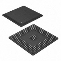


 工商网监
湘ICP备2023018690号
工商网监
湘ICP备2023018690号
