��������
��
�
������������ ������
�����
���������
SPRS294B − OCTOBER 2005 − REVISED JUNE 2006
D Highest-Performance Floating-Point Digital
D
D
D
D
D
D
Signal Processor (DSP): TMS320C6713B
− Eight 32-Bit Instructions/Cycle
− 32/64-Bit Data Word
− 300-, 225-, 200-MHz (GDP and ZDP), and
225-, 200-, 167-MHz (PYP) Clock Rates
− 3.3-, 4.4-, 5-, 6-Instruction Cycle Times
− 2400/1800, 1800/1350, 1600/1200, and
1336/1000 MIPS/MFLOPS
− Rich Peripheral Set, Optimized for Audio
− Highly Optimized C/C++ Compiler
− Extended Temperature Devices Available
Advanced Very Long Instruction Word
(VLIW) TMS320C67x DSP Core
− Eight Independent Functional Units:
− 2 ALUs (Fixed-Point)
− 4 ALUs (Floating-/Fixed-Point)
− 2 Multipliers (Floating-/Fixed-Point)
− Load-Store Architecture With 32 32-Bit
General-Purpose Registers
− Instruction Packing Reduces Code Size
− All Instructions Conditional
Instruction Set Features
− Native Instructions for IEEE 754
− Single- and Double-Precision
− Byte-Addressable (8-, 16-, 32-Bit Data)
− 8-Bit Overflow Protection
− Saturation; Bit-Field Extract, Set, Clear;
Bit-Counting; Normalization
L1/L2 Memory Architecture
− 4K-Byte L1P Program Cache
(Direct-Mapped)
− 4K-Byte L1D Data Cache (2-Way)
− 256K-Byte L2 Memory Total: 64K-Byte
L2 Unified Cache/Mapped RAM, and
192K-Byte Additional L2 Mapped RAM
Device Configuration
− Boot Mode: HPI, 8-, 16-, 32-Bit ROM Boot
− Endianness: Little Endian, Big Endian
32-Bit External Memory Interface (EMIF)
− Glueless Interface to SRAM, EPROM,
Flash, SBSRAM, and SDRAM
− 512M-Byte Total Addressable External
Memory Space
Enhanced Direct-Memory-Access (EDMA)
Controller (16 Independent Channels)
D 16-Bit Host-Port Interface (HPI)
D Two McASPs
D
D
D
D
D
D
D
D
D
D
D
− Two Independent Clock Zones Each
(1 TX and 1 RX)
− Eight Serial Data Pins Per Port:
Individually Assignable to any of the
Clock Zones
− Each Clock Zone Includes:
− Programmable Clock Generator
− Programmable Frame Sync Generator
− TDM Streams From 2-32 Time Slots
− Support for Slot Size:
8, 12, 16, 20, 24, 28, 32 Bits
− Data Formatter for Bit Manipulation
− Wide Variety of I2S and Similar Bit
Stream Formats
− Integrated Digital Audio Interface
Transmitter (DIT) Supports:
− S/PDIF, IEC60958-1, AES-3, CP-430
Formats
− Up to 16 transmit pins
− Enhanced Channel Status/User Data
− Extensive Error Checking and Recovery
Two Inter-Integrated Circuit Bus (I2C Bus)
Multi-Master and Slave Interfaces
Two Multichannel Buffered Serial Ports:
− Serial-Peripheral-Interface (SPI)
− High-Speed TDM Interface
− AC97 Interface
Two 32-Bit General-Purpose Timers
Dedicated GPIO Module With 16 pins
(External Interrupt Capable)
Flexible Phase-Locked-Loop (PLL) Based
Clock Generator Module
IEEE-1149.1 (JTAG†)
Boundary-Scan-Compatible
208-Pin PowerPAD PQFP (PYP)
272-BGA Packages (GDP and ZDP)
0.13-µm/6-Level Copper Metal Process
− CMOS Technology
3.3-V I/Os, 1.2‡-V Internal (GDP/ZDP/ PYP)
3.3-V I/Os, 1.4-V Internal (GDP/ZDP) [300
MHz]
Please be aware that an important notice concerning availability, standard warranty, and use in critical applications of
Texas Instruments semiconductor products and disclaimers thereto appears at the end of this data sheet.
TMS320C67x and PowerPAD are trademarks of Texas Instruments.
I2C Bus is a trademark of Philips Electronics N.V. Corporation
All trademarks are the property of their respective owners.
† IEEE Standard 1149.1-1990 Standard-Test-Access Port and Boundary Scan Architecture.
‡ These values are compatible with existing 1.26-V designs.
Copyright 2006, Texas Instruments Incorporated
���������� ���� �������!��� �" #$��%�! �" �� &$'(�#�!��� )�!%*
���)$#!" #������ !� "&%#���#�!���" &%� !+% !%��" �� �%,�" ��"!�$�%�!"
"!��)��) -�����!.* ���)$#!��� &��#%""��/ )�%" ��! �%#%""���(. ��#($)%
!%"!��/ �� �(( &����%!%�"*
POST OFFICE BOX 1443
• HOUSTON, TEXAS 77251−1443
1
���������
��
�
������������ ������
�����
���������
SPRS294B − OCTOBER 2005 − REVISED JUNE 2006
Table of Contents
revision history . . . . . . . . . . . . . . . . . . . . . . . . . . . . . . . . . . . . . . 3
GDP and ZDP 272-Ball BGA package (bottom view) . . . . . 5
PYP PowerPAD QFP package (top view) . . . . . . . . . . . . 10
description . . . . . . . . . . . . . . . . . . . . . . . . . . . . . . . . . . . . . . . . 11
device characteristics . . . . . . . . . . . . . . . . . . . . . . . . . . . . . . . 12
functional block and CPU (DSP core) diagram . . . . . . . . . . 13
CPU (DSP core) description . . . . . . . . . . . . . . . . . . . . . . . . . 14
memory map summary . . . . . . . . . . . . . . . . . . . . . . . . . . . . . . 16
peripheral register descriptions . . . . . . . . . . . . . . . . . . . . . . . 18
signal groups description . . . . . . . . . . . . . . . . . . . . . . . . . . . . 27
device configurations . . . . . . . . . . . . . . . . . . . . . . . . . . . . . . . 32
configuration examples . . . . . . . . . . . . . . . . . . . . . . . . . . . . . . 40
debugging considerations . . . . . . . . . . . . . . . . . . . . . . . . . . . 47
terminal functions . . . . . . . . . . . . . . . . . . . . . . . . . . . . . . . . . . 48
development support . . . . . . . . . . . . . . . . . . . . . . . . . . . . . . . . 64
device support . . . . . . . . . . . . . . . . . . . . . . . . . . . . . . . . . . . . . 65
CPU CSR register description . . . . . . . . . . . . . . . . . . . . . . . . 68
cache configuration (CCFG) register description . . . . . . . . 70
interrupts and interrupt selector . . . . . . . . . . . . . . . . . . . . . . . 71
external interrupt sources . . . . . . . . . . . . . . . . . . . . . . . . . . . . 73
EDMA module and EDMA selector . . . . . . . . . . . . . . . . . . . . 74
PLL and PLL controller . . . . . . . . . . . . . . . . . . . . . . . . . . . . . . 77
multichannel audio serial port (McASP) peripherals . . . . . 84
I2C . . . . . . . . . . . . . . . . . . . . . . . . . . . . . . . . . . . . . . . . . . . . . . . 89
general-purpose input/output (GPIO) . . . . . . . . . . . . . . . . . . 90
power-down mode logic . . . . . . . . . . . . . . . . . . . . . . . . . . . . .
power-supply sequencing . . . . . . . . . . . . . . . . . . . . . . . . . . . .
IEEE 1149.1 JTAG compatibility statement . . . . . . . . . . . . .
power-supply decoupling . . . . . . . . . . . . . . . . . . . . . . . . . . . .
2
POST OFFICE BOX 1443
91
93
95
94
EMIF device speed . . . . . . . . . . . . . . . . . . . . . . . . . . . . . . 95
EMIF big endian mode correctness . . . . . . . . . . . . . . . . 97
bootmode . . . . . . . . . . . . . . . . . . . . . . . . . . . . . . . . . . . . . . 98
reset . . . . . . . . . . . . . . . . . . . . . . . . . . . . . . . . . . . . . . . . . . . 98
absolute maximum ratings over operating case
temperature range . . . . . . . . . . . . . . . . . . . . . . . . . . 99
recommended operating conditions . . . . . . . . . . . . . . . . 99
electrical characteristics over recommended ranges of
supply voltage and operating case temperature 100
parameter measurement information . . . . . . . . . . . . . . 101
signal transition levels . . . . . . . . . . . . . . . . . . . . . . . . . . . 101
timing parameters and board routing analysis . . . . . . 103
input and output clocks . . . . . . . . . . . . . . . . . . . . . . . . . . 105
asynchronous memory timing . . . . . . . . . . . . . . . . . . . . 108
synchronous-burst memory timing . . . . . . . . . . . . . . . . . 111
synchronous DRAM timing . . . . . . . . . . . . . . . . . . . . . . . 113
HOLD/HOLDA timing . . . . . . . . . . . . . . . . . . . . . . . . . . . 119
BUSREQ timing . . . . . . . . . . . . . . . . . . . . . . . . . . . . . . . . 120
reset timing . . . . . . . . . . . . . . . . . . . . . . . . . . . . . . . . . . . . 121
external interrupt timing . . . . . . . . . . . . . . . . . . . . . . . . . 123
multichannel audio serial port (McASP) timing . . . . . . 124
inter-integrated circuits (I2C) timing . . . . . . . . . . . . . . . 127
host-port interface timing . . . . . . . . . . . . . . . . . . . . . . . . 129
multichannel buffered serial port timing . . . . . . . . . . . . 132
timer timing . . . . . . . . . . . . . . . . . . . . . . . . . . . . . . . . . . . . 142
general-purpose input/output (GPIO) port timing . . . . 143
JTAG test-port timing . . . . . . . . . . . . . . . . . . . . . . . . . . . 144
mechanical data . . . . . . . . . . . . . . . . . . . . . . . . . . . . . . . . 145
• HOUSTON, TEXAS 77251−1443
���������
��
�
������������ ������
�����
���������
SPRS294B − OCTOBER 2005 − REVISED JUNE 2006
REVISION HISTORY
The TMS320C6713B device-specific documentation has been split from TMS320C6713, TMS320C6713B Floating−Point Digital Signal Processors, literature number SPRS186K, into a separate Data Sheet, literature number
SPRS294. It also highlights technical changes made to SPRS294 to generate SPRS294A. These changes are
marked by “[Revision A].” Additionally, made changes to SPRS294A to generate SPRS294B. These changes
are marked by “[Revision B].” Both Revision A and B changes are noted in the Revision History table below.
Scope: Updated information on McASP, McBSP and JTAG for clarification. Changed Pin Description for A12 and
B11 (Revisions SPRS294 and SPRS294A). Updated Nomenclature figure by adding device−specific information
for the ZDP package. TI Recommends for new designs that the following pins be configured as such:
D Pin A12 connected directly to CVDD (core power)
D Pin B11 connected directly to Vss (ground)
PAGE(S)
NO.
ADDITIONS/CHANGES/DELETIONS
6
Terminal Assignments for the 272-Ball GDP and ZDP Packages (in Order of Ball No.) table:
Updated Signal Name for Ball No. A12
Updated Signal Name for Ball No. B11
10
PYP PowerPAD QFP package (top view):
Updated drawing
32
Device Configurations, device configurations at device reset section:
Updated “For proper device operation...” paragraph [Revision B]
33
Device Configurations, Device Configurations Pins at Device Reset (HD[4:3], HD8, HD12, and CLKMODE0) section:
Removed “CE1 width 32−bit” from Functional Description for “00” in HD[4:3](BOOTMODE) Configuration Pin
33
Device Configurations, Device Configurations Pins at Device Reset (HD[4:3], HD8, HD12, and CLKMODE0) section:
Updated “All other HD pins...” footnote [Revision B]
37
Table 22 Peripheral Pin Selection Matrix:
Updated/changed MCBSP0DIS (DEVCFG bit) from “ACLKKO” to “ACLKXO”
46
Configuration Example F (1 McBSP + HPI + 1 McASP) figure:
Updated from McBSP1DIS = 1 to McBSP1DIS = 0
47
Device Configurations, debugging considerations section:
Updated “Internal pullup/pulldown resistors...” paragraph [Revision B]
49
Terminal Functions, Resets and Interrupts section:
Updated IPU/IPD for RESET Signal Name from “IPU” to “−−”
50
Terminal Functions table, Host Port Interface section:
Removed “CE1 width 32−bit” from Description for “00” in Bootmode HD[4:3]
50
Terminal Functions table, Host Port Interface section:
Updated “Other HD pins...” paragraph [Revision B]
55
Terminal Functions, Timer 1 section:
Updated Description for TINP1/AHCLKX0 Signal Name
57
Terminal Functions, Reserved for Test section:
Updated Description for RSV Signal Name, 181 PYP, A12 GDP/ZDP
Updated Description for RSV Signal Name, 180 PYP, B11 GDP/ZDP
POST OFFICE BOX 1443
• HOUSTON, TEXAS 77251−1443
3
���������
��
�
������������ ������
�����
���������
SPRS294B − OCTOBER 2005 − REVISED JUNE 2006
PAGE(S)
NO.
57
Terminal Functions, Reserved for Test section:
Updated/changed Description for RSV Signal Name, A12 GDP (to “recommended”) − [Revision A]
Updated/changed Description for RSV Signal Name, B11 GDP (to “recommended”) − [Revision A]
57
Terminal Functions, Reserved for Test section:
Updated/changed Description for RSV Signal Name D12 to include PYP 178 as follows:
“...the D12/178 pin must be externally pulled down with a 10−kΩ resistor.” [Revision B]
66
Device Support, device and development-support tool nomenclature section:
Updated figure for clarity
67
Device Support, document support section:
Updated paragraphs for clarity
92
Power−Down Mode Logic − Triggering, Wake−up and Effects section:
Updated paragraphs [Revision B]
93
Power−Down Mode Logic − Triggering, Wake−up and Effects section, Characteristics of the Power-Down Modes table:
Added “It is recommended to use the PLLPWDN bit (PLLCSR.1) as an alternative to PD3” to PRWD Field (BITS 15−10) −
011100 − Effect on Chip’s Operation [Revision B]
93
Power−Down Mode Logic − Triggering, Wake−up and Effects section, Characteristics of the Power-Down Modes table:
Deleted three paragraphs following table [Revision B]
95
IEEE 1149.1 JTAG Compatibility Statement section:
Updated/added paragraphs for clarity
96
EMIF Device Speed section, Example Boards and Maximum EMIF Speed table:
Type − 3−Loads Short Traces, EMIF Interface Components section:
Updated from “32−Bit SDRAMs” to “16−Bit SDRAMs” [Revision B]
95
IEEE 1149.1 JTAG Compatibility Statement section:
Updated/added paragraphs for clarity
99
Recommended Operating Conditions:
Added VOS, Maximum voltage during overshoot row and associated footnote
Added VUS, Maximum voltage during undershoot row and associated footnote
102
Parameter Measurement Information, AC transient rise/fall time specifications section:
Added AC Transient Specification Rise Time figure
Added AC Transient Specification Fall Time figure
124
MULTICHANNEL AUDIO SERIAL PORT (McASP) TIMING:
timing requirements for McASP section:
Updated Parameter No. 3, tc(ACKRX), from “33” to “greater of 2P or 33 ns” and added associated footnote
124
MULTICHANNEL AUDIO SERIAL PORT (McASP) TIMING:
switching characteristics over recommended operating conditions for McASP section:
Updated Parameter No. 11, tc(ACKRX), from “33” to “greater of 2P or 33 ns” and added associated footnote
125, 126
4
ADDITIONS/CHANGES/DELETIONS
MULTICHANNEL AUDIO SERIAL PORT (McASP) TIMING section:
Updated McASP Input and Output drawings
134
MULTICHANNEL BUFFERED SERIAL PORT TIMING section:
switching characteristics over recommended operating conditions for McBSP section:
Updated McBSP Timings figure
147
Mechanical Data section:
Added statement to the Packaging Information section
POST OFFICE BOX 1443
• HOUSTON, TEXAS 77251−1443
���������
��
�
������������ ������
�����
���������
SPRS294B − OCTOBER 2005 − REVISED JUNE 2006
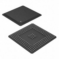
GDP and ZDP 272-Ball BGA package (bottom view)
>
0��
0��
��
<
���
���>
���
�0��
��
��4
��
1���
��
1��
�
1����;
��5�6
0��
��
2
��
�
��
<
�0��
����
0��
0��
?
0��
�0��
�0��
��
0��
���
��2
���
�0��
���;
�����;
����
0��
�0��
��
��
�
��
3
0��
��
4
��
�0��
0��
0
����
��
4
�0��
��
�
���
���
���
��3
��<
��
�
���;
�����;
�����
�?�;
��?�;
��?�
�0��
��
�
�0��
��
���
�0��
�0��
���
�
����
���
����
0��
�0��
�0��
�0��
0��
0��
�0��
�0��
�0��
0��
�0��
�0��
�0��
0��
���
��
0��
�
���2
���3
�0��
0��
0��
��
�
��
3
��
2
�
�0��
���
����
�0��
�0��
�0��
��
��
�
�
���<
���4
����
0��
0��
��4
0��
��
�
�
��
�
����
���
0��
0��
���
��
��<
�
�
1�
;
�8��5�6
��
;
���
���
;
�8��5 6
0��
0��
0��
0��
0��
0��
�0��
��2
��3
��8
�8
;
�8��536
�
18
;
������
�0��
0��
0��
0��
0��
�0��
���
���
�0��
1
�0��
0��
�
1��;
�=�
1��
�0��
0��
0��
0��
0��
�0��
���
��
0��
@
���;
�8��5�6
�0��
����;
�����
0��
0��
0��
0��
0��
=�
�
=�
��
���
��A
=���;
��5
6
=
��8�;
���8�
�8�;
�8��5
6
�
1��;
��
1��
0��
0��
�0��
=��>;
��
1�
==?�
;
����
�
�����;
�8��5�6
�����;
�8��5�6
�
18�;
��
18�
0��
0��
=���
�;
�8�
5�6
=���
;
�8�
5
6
=�;?;
�8�
5�6
�
����
;
�8��526
����
;
�=�
18�
�0��
�0��
�0��
=���;
�8�
536
0��
=��;
�8�
5�6
�
�
1�
;
��
0��
��5 6
7�8�9��� :
0��
0��
=��;
��
18
=��
;
�8�
5�6
=��;
�8�
526
�
�0��
��5�6
7�8�9����:
����
0��
�0��
�0��
��0
0��
����
�
1����
�0��
��0
0��
�0��
�0��
�0��
0��
=��;
���8
�0��
=�
;
�8�
5 6
��536
��526;
� 7�8�9���3:; 7�8�9���2:;
�������� �������
�0��
�
1
�����
�
=0
0��
�0��
0��
0��
�0��
���2
��0
���
=�
2;
��5
26
=�
�;
��5
�6
=�4;
��546
=��;
�=�
1�
�0��
=�2;
��5�6
=��;
�����
�
0��
�0��
�0��
0��
��0
����
���
�0��
���
����
��0
���3
�0��
=�
3;
��5
36
0��
=�
�;
��5
�6
=�