www.ti.com
TMS320F28379D, TMS320F28379D-Q1, TMS320F28378D, TMS320F28377D
TMS320F28379D,
TMS320F28379D-Q1,
TMS320F28377D-Q1,
TMS320F28376D, TMS320F28378D,
TMS320F28375D, TMS320F28377D
TMS320F28374D
TMS320F28377D-Q1, TMS320F28376D,
TMS320F28375D,
TMS320F28374D
SPRS880O – DECEMBER
2013 – REVISED
FEBRUARY 2021
SPRS880O – DECEMBER 2013 – REVISED FEBRUARY 2021
TMS320F2837xD Dual-Core Microcontrollers
1 Features
•
•
•
•
•
•
•
Dual-core architecture
– Two TMS320C28x 32-bit CPUs
– 200 MHz
– IEEE 754 single-precision Floating-Point Unit
(FPU)
– Trigonometric Math Unit (TMU)
– Viterbi/Complex Math Unit (VCU-II)
Two programmable Control Law Accelerators
(CLAs)
– 200 MHz
– IEEE 754 single-precision floating-point
instructions
– Executes code independently of main CPU
On-chip memory
– 512KB (256KW) or 1MB (512KW) of flash
(ECC-protected)
– 172KB (86KW) or 204KB (102KW) of RAM
(ECC-protected or parity-protected)
– Dual-zone security supporting third-party
development
– Unique identification number
Clock and system control
– Two internal zero-pin 10-MHz oscillators
– On-chip crystal oscillator
– Windowed watchdog timer module
– Missing clock detection circuitry
1.2-V core, 3.3-V I/O design
System peripherals
– Two External Memory Interfaces (EMIFs) with
ASRAM and SDRAM support
– Dual 6-channel Direct Memory Access (DMA)
controllers
– Up to 169 individually programmable,
multiplexed General-Purpose Input/Output
(GPIO) pins with input filtering
– Expanded Peripheral Interrupt controller (ePIE)
– Multiple Low-Power Mode (LPM) support with
external wakeup
Communications peripherals
– USB 2.0 (MAC + PHY)
– Support for 12-pin 3.3 V-compatible Universal
Parallel Port (uPP) interface
– Two Controller Area Network (CAN) modules
(pin-bootable)
•
•
– Three high-speed (up to 50-MHz) SPI ports
(pin-bootable)
– Two Multichannel Buffered Serial Ports
(McBSPs)
– Four Serial Communications Interfaces (SCI/
UART) (pin-bootable)
– Two I2C interfaces (pin-bootable)
Analog subsystem
– Up to four Analog-to-Digital Converters (ADCs)
• 16-bit mode
– 1.1 MSPS each (up to 4.4-MSPS system
throughput)
– Differential inputs
– Up to 12 external channels
• 12-bit mode
– 3.5 MSPS each (up to 14-MSPS system
throughput)
– Single-ended inputs
– Up to 24 external channels
• Single Sample-and-Hold (S/H) on each ADC
• Hardware-integrated post-processing of
ADC conversions
– Saturating offset calibration
– Error from setpoint calculation
– High, low, and zero-crossing compare,
with interrupt capability
– Trigger-to-sample delay capture
– Eight windowed comparators with 12-bit Digitalto-Analog Converter (DAC) references
– Three 12-bit buffered DAC outputs
Enhanced control peripherals
– 24 Pulse Width Modulator (PWM) channels with
enhanced features
– 16 High-Resolution Pulse Width Modulator
(HRPWM) channels
• High resolution on both A and B channels of
8 PWM modules
• Dead-band support (on both standard and
high resolution)
– Six Enhanced Capture (eCAP) modules
– Three Enhanced Quadrature Encoder Pulse
(eQEP) modules
– Eight Sigma-Delta Filter Module (SDFM) input
channels, 2 parallel filters per channel
• Standard SDFM data filtering
An©IMPORTANT
NOTICEIncorporated
at the end of this data sheet addresses availability, warranty, changes, use in
safety-critical
applications,
Copyright
2021 Texas Instruments
Submit
Document
Feedback
intellectual property matters and other important disclaimers. PRODUCTION DATA.
Product Folder Links: TMS320F28379D TMS320F28379D-Q1 TMS320F28378D TMS320F28377D
TMS320F28377D-Q1 TMS320F28376D TMS320F28375D TMS320F28374D
1
�TMS320F28379D, TMS320F28379D-Q1, TMS320F28378D, TMS320F28377D
TMS320F28377D-Q1, TMS320F28376D, TMS320F28375D, TMS320F28374D
www.ti.com
SPRS880O – DECEMBER 2013 – REVISED FEBRUARY 2021
•
•
•
•
•
•
Comparator filter for fast action for out of
range
Configurable Logic Block (CLB)
– Augments existing peripheral capability
– Supports position manager solutions
Functional Safety-Compliant
– Developed for functional safety applications
– Documentation available to aid ISO 26262
system design up to ASIL D; IEC 61508 up to
SIL 3; IEC 60730 up to Class C; and UL 1998
up to Class 2
– Hardware integrity up to ASIL B, SIL 2
Safety-related certification
– ISO 26262 certified up to ASIL B and IEC
61508 certified up to SIL 2 by TUV SUD
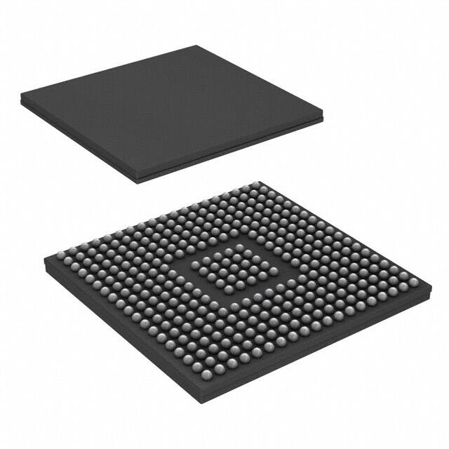
Package options:
– Lead-free, green packaging
– 337-ball New Fine Pitch Ball Grid Array
(nFBGA) [ZWT suffix]
– 176-pin PowerPAD™ Thermally Enhanced LowProfile Quad Flatpack (HLQFP) [PTP suffix]
– 100-pin PowerPAD Thermally Enhanced Thin
Quad Flatpack (HTQFP) [PZP suffix]
Temperature options:
– T: –40°C to 105°C junction
– S: –40°C to 125°C junction
– Q: –40°C to 125°C free-air
(AEC Q100 qualification for automotive
applications)
2 Applications
•
•
•
•
•
•
•
•
•
•
•
•
•
•
•
•
•
•
•
•
Medium/short range radar
Traction inverter motor control
HVAC large commercial motor control
Automated sorting equipment
CNC control
AC charging (pile) station
DC charging (pile) station
EV charging station power module
Energy storage power conversion system (PCS)
Central inverter
Solar power optimizer
String inverter
Inverter & motor control
On-board (OBC) & wireless charger
Linear motor segment controller
Servo drive control module
AC-input BLDC motor drive
DC-input BLDC motor drive
Industrial AC-DC
Three phase UPS
3 Description
C2000™ 32-bit microcontrollers are optimized for processing, sensing, and actuation to improve closed-loop
performance in real-time control applications such as industrial motor drives; solar inverters and digital power;
electrical vehicles and transportation; motor control; and sensing and signal processing. The C2000 line includes
the Premium performance MCUs and the Entry performance MCUs.
The TMS320F2837xD is a powerful 32-bit floating-point microcontroller unit (MCU) designed for advanced
closed-loop control applications such as industrial motor drives; solar inverters and digital power; electrical
vehicles and transportation; and sensing and signal processing. To accelerate application development, the
DigitalPower software development kit (SDK) for C2000 MCUs and the MotorControl software development kit
(SDK) for C2000™ MCUs are available. The F2837xD supports a new dual-core C28x architecture that
significantly boosts system performance. The integrated analog and control peripherals also let designers
consolidate control architectures and eliminate multiprocessor use in high-end systems.
The dual real-time control subsystems are based on TI’s 32-bit C28x floating-point CPUs, which provide
200 MHz of signal processing performance in each core. The C28x CPUs are further boosted by the new TMU
accelerator, which enables fast execution of algorithms with trigonometric operations common in transforms and
torque loop calculations; and the VCU accelerator, which reduces the time for complex math operations common
in encoded applications.
The F2837xD microcontroller family features two CLA real-time control coprocessors. The CLA is an
independent 32-bit floating-point processor that runs at the same speed as the main CPU. The CLA responds to
peripheral triggers and executes code concurrently with the main C28x CPU. This parallel processing capability
can effectively double the computational performance of a real-time control system. By using the CLA to service
time-critical functions, the main C28x CPU is free to perform other tasks, such as communications and
diagnostics. The dual C28x+CLA architecture enables intelligent partitioning between various system tasks. For
2
Submit Document Feedback
Copyright © 2021 Texas Instruments Incorporated
Product Folder Links: TMS320F28379D TMS320F28379D-Q1 TMS320F28378D TMS320F28377D
TMS320F28377D-Q1 TMS320F28376D TMS320F28375D TMS320F28374D
�TMS320F28379D, TMS320F28379D-Q1, TMS320F28378D, TMS320F28377D
TMS320F28377D-Q1, TMS320F28376D, TMS320F28375D, TMS320F28374D
www.ti.com
SPRS880O – DECEMBER 2013 – REVISED FEBRUARY 2021
example, one C28x+CLA core can be used to track speed and position, while the other C28x+CLA core can be
used to control torque and current loops.
The TMS320F2837xD supports up to 1MB (512KW) of onboard flash memory with error correction code (ECC)
and up to 204KB (102KW) of SRAM. Two 128-bit secure zones are also available on each CPU for code
protection.
Performance analog and control peripherals are also integrated on the F2837xD MCU to further enable system
consolidation. Four independent 16-bit ADCs provide precise and efficient management of multiple analog
signals, which ultimately boosts system throughput. The new sigma-delta filter module (SDFM) works in
conjunction with the sigma-delta modulator to enable isolated current shunt measurements. The Comparator
Subsystem (CMPSS) with windowed comparators allows for protection of power stages when current limit
conditions are exceeded or not met. Other analog and control peripherals include DACs, PWMs, eCAPs,
eQEPs, and other peripherals.
Peripherals such as EMIFs, CAN modules (ISO 11898-1/CAN 2.0B-compliant), and a new uPP interface extend
the connectivity of the F2837xD. The uPP interface is a new feature of the C2000™ MCUs and supports highspeed parallel connection to FPGAs or other processors with similar uPP interfaces. Lastly, a USB 2.0 port with
MAC and PHY lets users easily add universal serial bus (USB) connectivity to their application.
To learn more about the C2000 MCUs, visit the C2000 Overview at www.ti.com/c2000.
Device Information
PART NUMBER(1)
PACKAGE
BODY SIZE
TMS320F28379DZWT
nFBGA (337)
16.0 mm × 16.0 mm
TMS320F28377DZWT
nFBGA (337)
16.0 mm × 16.0 mm
TMS320F28376DZWT
nFBGA (337)
16.0 mm × 16.0 mm
TMS320F28375DZWT
nFBGA (337)
16.0 mm × 16.0 mm
TMS320F28374DZWT
nFBGA (337)
16.0 mm × 16.0 mm
TMS320F28379DPTP
HLQFP (176)
24.0 mm × 24.0 mm
TMS320F28378DPTP
HLQFP (176)
24.0 mm × 24.0 mm
TMS320F28377DPTP
HLQFP (176)
24.0 mm × 24.0 mm
TMS320F28376DPTP
HLQFP (176)
24.0 mm × 24.0 mm
TMS320F28375DPTP
HLQFP (176)
24.0 mm × 24.0 mm
TMS320F28374DPTP
HLQFP (176)
24.0 mm × 24.0 mm
TMS320F28375DPZP
HTQFP (100)
14.0 mm × 14.0 mm
(1)
For more information on these devices, see Mechanical, Packaging, and Orderable Information.
Copyright © 2021 Texas Instruments Incorporated
Submit Document Feedback
Product Folder Links: TMS320F28379D TMS320F28379D-Q1 TMS320F28378D TMS320F28377D
TMS320F28377D-Q1 TMS320F28376D TMS320F28375D TMS320F28374D
3
�TMS320F28379D, TMS320F28379D-Q1, TMS320F28378D, TMS320F28377D
TMS320F28377D-Q1, TMS320F28376D, TMS320F28375D, TMS320F28374D
www.ti.com
SPRS880O – DECEMBER 2013 – REVISED FEBRUARY 2021
4 Functional Block Diagram
Figure 4-1 shows the CPU system and associated peripherals.
PSWD
Dual
Code
Security
Module
+
Emulation
Code
Security
Logic
(ECSL)
Secure Memories
shown in Red
User
Configurable
DCSM
OTP
1K x 16
User
Configurable
DCSM
PSWD
OTP
1K x 16
FLASH
FLASH
256K x 16
Secure
256K x 16
Secure
PUMP
Dual
Code
Security
Module
+
Emulation
Code
Security
Logic
(ECSL)
CPU2.CLA1
OTP/Flash
Wrapper
OTP/Flash
Wrapper
MEMCPU1
MEMCPU2
CPU1.M0 RAM 1Kx16
CPU1.CLA1 to CPU1
128x16 MSG RAM
CPU1 to CPU1.CLA1
128x16 MSG RAM
CPU1.M1 RAM 1Kx16
C28 CPU-2
FPU
VCU-II
TMU
CPU2.M0 RAM 1Kx16
FPU
VCU-II
TMU
CPU2.M1 RAM 1Kx16
CPU1 Local Shared
6x 2Kx16
LS0-LS5 RAMs
CPU1.D1 RAM 2Kx16
WD Timer
NMI-WDT
CPU1.CLA1 Data ROM
(4Kx16)
16-/12-bit ADC
x4
A5:0
A
B
D
Config
D5:0
ADCIN14
ADCIN15
Data Bus
Bridge
Comparator
DAC
Subsystem
x3
(CMPSS)
CPU Timer 0
CPU Timer 1
CPU Timer 2
External Crystal or
Oscillator
Secure-ROM 32Kx16
Secure
Aux PLL
AUXCLKIN
Boot-ROM 32Kx16
Nonsecure
ePIE
(up to 192
interrupts)
TRST
TCK
CPU2.DMA
JTAG
TDI
TMS
TDO
GPIO
GPIOn
EMIF2
EM2Dx
EMIF1
EM2Ax
Data Bus
Bridge
EM2CTLx
Data Bus
Bridge
EM1Dx
UPPAST
UPPACLK
UPPAEN
MFSXx
MFSRx
UPPAWT
RAM
uPP
UPPAD[7:0]
MCLKXx
MCLKRx
MDXx
MDRx
SPISTEx
SPICLKx
SPISIMOx
SPISOMIx
McBSPA/B
Data Bus
Bridge
EM1Ax
SPIA/B/C
(16L FIFO)
Peripheral Frame 2
EM1CTLx
CANA/B
(32-MBOX)
CANTXx
USB
Ctrl /
PHY
CANRXx
SCITXDx
SDx_Cy
SDx_Dy
EQEPxI
EQEPxS
I2C-A/B
(16L FIFO)
Data Bus
Bridge
USBDP
SCIA/B/C/D
(16L FIFO)
SCLx
SDFM-1/2
Data Bus
Bridge
USBDM
Data Bus Bridge
eQEP-1/2/3
EQEPxB
ECAPx
eCAP1/../6
EXTSYNCOUT
EPWMxB
EXTSYNCIN
EPWMxA
TZ1-TZ6
INTOSC2
CPU2 Buses
EQEPxA
ePWM-1/../12
Main PLL
CPU2.CLA1 Data ROM
(4Kx16)
CPU1 Buses
Peripheral Frame 1
HRPWM-1/../8
(CPU1 only)
CPU2.D1 RAM 2Kx16
WD Timer
NMI-WDT
CPU2 to CPU1
1Kx16 MSG RAM
CPU1.DMA
INTOSC1
CPU2.D0 RAM 2Kx16
CPU1 to CPU2
1Kx16 MSG RAM
ePIE
(up to 192
interrupts)
SDAx
Analog
MUX
Boot-ROM 32Kx16
Nonsecure
ADC
Result
Regs
SCIRXDx
C5:2
C
CPU1.CLA1 Bus
B5:0
Watchdog 1/2
CPU2 Local Shared
6x 2Kx16
LS0-LS5 RAMs
Global Shared
16x 4Kx16
GS0-GS15 RAMs
CPU Timer 0
CPU Timer 1
CPU Timer 2
Secure-ROM 32Kx16
Secure
GPIO MUX
CPU2.CLA1 to CPU2
128x16 MSG RAM
Interprocessor
Communication
(IPC)
Module
CPU1.D0 RAM 2Kx16
Low-Power
Mode Control
CPU2 to CPU2.CLA1
128x16 MSG RAM
CPU2.CLA1 Bus
CPU1.CLA1
C28 CPU-1
GPIO MUX, Input X-BAR, Output X-BAR
Figure 4-1. Functional Block Diagram
4
Submit Document Feedback
Copyright © 2021 Texas Instruments Incorporated
Product Folder Links: TMS320F28379D TMS320F28379D-Q1 TMS320F28378D TMS320F28377D
TMS320F28377D-Q1 TMS320F28376D TMS320F28375D TMS320F28374D
�TMS320F28379D, TMS320F28379D-Q1, TMS320F28378D, TMS320F28377D
TMS320F28377D-Q1, TMS320F28376D, TMS320F28375D, TMS320F28374D
www.ti.com
SPRS880O – DECEMBER 2013 – REVISED FEBRUARY 2021
Table of Contents
1 Features............................................................................1
2 Applications..................................................................... 2
3 Description.......................................................................2
4 Functional Block Diagram.............................................. 4
5 Revision History.............................................................. 6
6 Device Comparison......................................................... 7
6.1 Related Products........................................................ 9
7 Terminal Configuration and Functions........................10
7.1 Pin Diagrams............................................................ 10
7.2 Signal Descriptions................................................... 17
7.3 Pins With Internal Pullup and Pulldown.................... 40
7.4 Pin Multiplexing.........................................................41
7.5 Connections for Unused Pins................................... 48
8 Specifications................................................................ 49
8.1 Absolute Maximum Ratings...................................... 49
8.2 ESD Ratings – Commercial...................................... 50
8.3 ESD Ratings – Automotive....................................... 50
8.4 Recommended Operating Conditions.......................51
8.5 Power Consumption Summary................................. 52
8.6 Electrical Characteristics...........................................57
8.7 Thermal Resistance Characteristics......................... 58
8.8 Thermal Design Considerations................................59
8.9 System...................................................................... 60
8.10 Analog Peripherals..................................................95
8.11 Control Peripherals............................................... 125
8.12 Communications Peripherals................................ 144
9 Detailed Description....................................................177
9.1 Overview................................................................. 177
9.2 Functional Block Diagram....................................... 177
9.3 Memory................................................................... 179
Copyright © 2021 Texas Instruments Incorporated
9.4 Identification............................................................187
9.5 Bus Architecture – Peripheral Connectivity.............188
9.6 C28x Processor...................................................... 189
9.7 Control Law Accelerator..........................................192
9.8 Direct Memory Access............................................ 193
9.9 Interprocessor Communication Module.................. 195
9.10 Boot ROM and Peripheral Booting........................196
9.11 Dual Code Security Module.................................. 199
9.12 Timers................................................................... 200
9.13 Nonmaskable Interrupt With Watchdog Timer
(NMIWD)................................................................... 200
9.14 Watchdog.............................................................. 201
9.15 Configurable Logic Block (CLB)............................202
9.16 Functional Safety.................................................. 204
10 Applications, Implementation, and Layout............. 206
10.1 TI Reference Design............................................. 206
11 Device and Documentation Support........................207
11.1 Device and Development Support Tool
Nomenclature............................................................ 207
11.2 Markings................................................................208
11.3 Tools and Software................................................209
11.4 Documentation Support.........................................211
11.5 Support Resources................................................211
11.6 Trademarks........................................................... 212
11.7 Electrostatic Discharge Caution............................ 212
11.8 Glossary................................................................ 212
12 Mechanical, Packaging, and Orderable
Information.................................................................. 213
12.1 Packaging Information.......................................... 213
Submit Document Feedback
Product Folder Links: TMS320F28379D TMS320F28379D-Q1 TMS320F28378D TMS320F28377D
TMS320F28377D-Q1 TMS320F28376D TMS320F28375D TMS320F28374D
5
�TMS320F28379D, TMS320F28379D-Q1, TMS320F28378D, TMS320F28377D
TMS320F28377D-Q1, TMS320F28376D, TMS320F28375D, TMS320F28374D
www.ti.com
SPRS880O – DECEMBER 2013 – REVISED FEBRUARY 2021
5 Revision History
Changes from November 17, 2020 to January 31, 2021 (from Revision N (November 2020) to
Revision O (January 2021))
Page
• Device Comparison: Updated part numbers.......................................................................................................7
• ESD Ratings – Commercial: Updated part numbers........................................................................................ 50
• ESD Ratings – Automotive: Updated part numbers......................................................................................... 50
• Device and Development Support Tool Nomenclature: Updated Device Nomenclature image to show -Q1 part
number............................................................................................................................................................207
6
Submit Document Feedback
Copyright © 2021 Texas Instruments Incorporated
Product Folder Links: TMS320F28379D TMS320F28379D-Q1 TMS320F28378D TMS320F28377D
TMS320F28377D-Q1 TMS320F28376D TMS320F28375D TMS320F28374D
�TMS320F28379D, TMS320F28379D-Q1, TMS320F28378D, TMS320F28377D
TMS320F28377D-Q1, TMS320F28376D, TMS320F28375D, TMS320F28374D
www.ti.com
SPRS880O – DECEMBER 2013 – REVISED FEBRUARY 2021
6 Device Comparison
Table 6-1 lists the features of each 2837xD device.
Table 6-1. Device Comparison
FEATURE(1)
Package Type
(ZWT is an nFBGA package.
PTP is an HLQFP package.
PZP is an HTQFP package.)
28379D
28379D-Q1
28378D
337-Ball 176-Pin
ZWT
PTP
176-Pin
PTP
28377D
28377D-Q1
28376D
28375D
337-Ball 176-Pin 337-Ball 176-Pin 337-Ball 176-Pin
ZWT
PTP
ZWT
PTP
ZWT
PTP
28374D
100-Pin 337-Ball 176-Pin
PZP
ZWT
PTP
Processor and Accelerators
Number
C28x
CLA – Type 1
2
Frequency (MHz)
200
Floating-Point Unit (FPU)
Yes
VCU-II
Yes
TMU – Type 0
Yes
Number
2
Frequency (MHz)
200
6-Channel DMA – Type 0
2
Memory
1MB (512KW)
[512KB (256KW)
per CPU]
Flash (16-bit words)
1MB (512KW)
[512KB (256KW)
per CPU]
1MB (512KW)
[512KB (256KW)
per CPU]
Dedicated and Local Shared
RAM
RAM (16-bit
words)
Global Shared RAM
1MB (512KW)
[512KB (256KW) per CPU]
512KB (256KW)
[256KB (128KW)
per CPU]
128KB (64KW)
96KB (48KW)
204KB (102KW)
172KB (86KW)
72KB (36KW)
[36KB (18KW) per CPU]
128KB (64KW)
128KB (64KW)
128KB (64KW)
96KB (48KW)
4KB (2KW)
[2KB (1KW) per CPU]
Message RAM
Total RAM
512KB (256KW)
[256KB (128KW)
per CPU]
204KB (102KW)
204KB (102KW)
204KB (102KW)
172KB (86KW)
Code security for on-chip flash, RAM, and OTP
blocks
Yes
Boot ROM
Yes
System
Configurable Logic Block (CLB)
4 tiles
No
32-bit CPU timers
6 (3 per CPU)
Watchdog timers
2 (1 per CPU)
Nonmaskable Interrupt Watchdog (NMIWD) timers
2 (1 per CPU)
Crystal oscillator/External clock input
1
0-pin internal oscillator
I/O pins (shared)
2
GPIO
169
97
97
169
97
169
External interrupts
EMIF
97
169
–
1
97
41
169
97
5
EMIF1 (16-bit or 32-bit)
EMIF2 (16-bit)
1
1
–
–
1
1
–
1
–
–
–
1
1
–
Analog Peripherals
ADC 16-bit mode
MSPS
1.1
–
1.1
–
Conversion Time (ns)(2)
915
–
915
–
Input pins
24
20
–
24
20
24
20
–
Channels (differential)
12
9
–
12
9
12
9
–
MSPS
ADC 12-bit mode
3.5
Conversion Time (ns)(2)
280
Input pins
24
20
20
24
20
24
20
24
20
14
24
20
Channels (single-ended)
24
20
20
24
20
24
20
24
20
14
24
20
Number of 16-bit or 12-bit ADCs
4
–
4
Number of 12-bit only ADCs
–
4
–
Temperature sensor
–
4
2
4
8
4
8
1
CMPSS (each CMPSS has two comparators and
two internal DACs)
8
Buffered DAC
3
Control Peripherals (3)
eCAP inputs – Type 0
6
Copyright © 2021 Texas Instruments Incorporated
Submit Document Feedback
Product Folder Links: TMS320F28379D TMS320F28379D-Q1 TMS320F28378D TMS320F28377D
TMS320F28377D-Q1 TMS320F28376D TMS320F28375D TMS320F28374D
7
�TMS320F28379D, TMS320F28379D-Q1, TMS320F28378D, TMS320F28377D
TMS320F28377D-Q1, TMS320F28376D, TMS320F28375D, TMS320F28374D
www.ti.com
SPRS880O – DECEMBER 2013 – REVISED FEBRUARY 2021
Table 6-1. Device Comparison (continued)
FEATURE(1)
Package Type
(ZWT is an nFBGA package.
PTP is an HLQFP package.
PZP is an HTQFP package.)
28379D
28379D-Q1
28378D
337-Ball 176-Pin
ZWT
PTP
176-Pin
PTP
Enhanced Pulse Width Modulator (ePWM)
channels – Type 4
28377D
28377D-Q1
28376D
28375D
337-Ball 176-Pin 337-Ball 176-Pin 337-Ball 176-Pin
ZWT
PTP
ZWT
PTP
ZWT
PTP
24
28374D
100-Pin 337-Ball 176-Pin
PZP
ZWT
PTP
24
15
24
eQEP modules – Type 0
3
3
2
3
High-resolution ePWM channels – Type 4
16
16
9
16
8
8
6
8
4
3
4
Yes
No
Yes
SDFM channels – Type 0
Communication Peripherals (3)
Controller Area Network (CAN) – Type 0(4)
2
Inter-Integrated Circuit (I2C) – Type 0
2
Multichannel Buffered Serial Port (McBSP) –
Type 1
2
SCI - Type 0
4
Serial Peripheral Interface (SPI) – Type 2
3
USB – Type 0
1
uPP – Type 0
1
Temperature and Qualification
T: –40°C to 105°C
Junction
Temperature (TJ)
Free-Air
Temperature (TA)
(1)
(2)
(3)
(4)
(5)
8
Yes
No
Yes
S: –40°C to 125°C
Yes
Q: –40°C to 150°C(5)
Yes
Yes
No
Yes
No
Q: –40°C to 125°C(5)
Yes
Yes
No
Yes
No
A type change represents a major functional feature difference in a peripheral module. Within a peripheral type, there may be minor
differences between devices that do not affect the basic functionality of the module. For more information, see the C2000 Real-Time
Control Peripherals Reference Guide.
Time between start of sample-and-hold window to start of sample-and-hold window of the next conversion.
For devices that are available in more than one package, the peripheral count listed in the smaller package is reduced because the
smaller package has less device pins available. The number of peripherals internally present on the device is not reduced compared to
the largest package offered within a part number. See Section 7 to identify which peripheral instances are accessible on pins in the
smaller package.
The CAN module uses the IP known as D_CAN. This document uses the names CAN and D_CAN interchangeably to reference this
peripheral.
The letter Q refers to AEC Q100 qualification for automotive applications.
Submit Document Feedback
Copyright © 2021 Texas Instruments Incorporated
Product Folder Links: TMS320F28379D TMS320F28379D-Q1 TMS320F28378D TMS320F28377D
TMS320F28377D-Q1 TMS320F28376D TMS320F28375D TMS320F28374D
�TMS320F28379D, TMS320F28379D-Q1, TMS320F28378D, TMS320F28377D
TMS320F28377D-Q1, TMS320F28376D, TMS320F28375D, TMS320F28374D
www.ti.com
SPRS880O – DECEMBER 2013 – REVISED FEBRUARY 2021
6.1 Related Products
For information about similar products, see the following links:
TMS320F2837xD Microcontrollers
The F2837xD series sets a new standard for performance with dual subsystems. Each subsystem consists of a
C28x CPU and a parallel control law accelerator (CLA), each running at 200 MHz. Enhancing performance are
TMU and VCU accelerators. New capabilities include multiple 16-bit/12-bit mode ADCs, DAC, Sigma-Delta
filters, USB, configurable logic block (CLB), on-chip oscillators, and enhanced versions of all peripherals. The
F2837xD is available with up to 1MB of Flash. It is available in a 176-pin QFP or 337-pin BGA package.
TMS320F2837xS Microcontrollers
The F2837xS series is a pin-to-pin compatible version of F2837xD but with only one C28x-CPU-and-CLA
subsystem enabled. It is also available in a 100-pin QFP to enable compatibility with the TMS320F2807x series.
Copyright © 2021 Texas Instruments Incorporated
Submit Document Feedback
Product Folder Links: TMS320F28379D TMS320F28379D-Q1 TMS320F28378D TMS320F28377D
TMS320F28377D-Q1 TMS320F28376D TMS320F28375D TMS320F28374D
9
�TMS320F28379D, TMS320F28379D-Q1, TMS320F28378D, TMS320F28377D
TMS320F28377D-Q1, TMS320F28376D, TMS320F28375D, TMS320F28374D
www.ti.com
SPRS880O – DECEMBER 2013 – REVISED FEBRUARY 2021
7 Terminal Configuration and Functions
7.1 Pin Diagrams
Figure 7-1 to Figure 7-4 show the terminal assignments on the 337-ball ZWT New Fine Pitch Ball Grid Array.
Each figure shows a quadrant of the terminal assignments. Figure 7-5 shows the pin assignments on the 176-pin
PTP PowerPAD Thermally Enhanced Low-Profile Quad Flatpack. Figure 7-6 shows the pin assignments on the
100-pin PZP PowerPAD Thermally Enhanced Thin Quad Flatpack.
1
2
3
4
5
6
7
8
9
10
W
VSSA
ADCINB1
ADCINB3
ADCINB5
VREFHIB
VREFLOD
VSS
VDDIO
GPIO128
GPIO116
W
V
VREFHIA
ADCINB0
ADCINB2
ADCINB4
VREFHID
VREFLOB
VSSA
GPIO124
GPIO127
GPIO131
V
U
ADCINA0
ADCINA2
ADCINA4
ADCIN15
ADCIND1
ADCIND3
ADCIND5
GPIO123
GPIO126
GPIO130
U
T
ADCINA1
ADCINA3
ADCINA5
ADCIN14
ADCIND0
ADCIND2
ADCIND4
GPIO122
GPIO125
GPIO129
T
R
VREFHIC
VREFLOA
ADCINC2
ADCINC4
VSSA
VDDA
VSS
VSS
VDDIO
VDD
R
P
VSSA
VREFLOC
ADCINC3
ADCINC5
VSSA
VDDA
VSS
VSS
VDDIO
VDD
P
7
8
9
10
N
VSS
GPIO109
GPIO114
GPIO113
VSS
VSS
N
M
VDDIO
GPIO110
GPIO112
GPIO111
VDDIO
VDDIO
M
VSS
VSS
VSS
M
L
GPIO27
GPIO106
GPIO107
GPIO108
VSS
VSS
L
VSS
VSS
VSS
L
K
GPIO26
GPIO25
GPIO24
GPIO23
VDD
VDD
K
VSS
VSS
VSS
K
1
2
3
4
5
6
8
9
10
A. Only the GPIO function is shown on GPIO terminals. See Section 7.2.1 for the complete, muxed signal name.
Figure 7-1. 337-Ball ZWT New Fine Pitch Ball Grid Array (Bottom View) – [Quadrant A]
10
Submit Document Feedback
Copyright © 2021 Texas Instruments Incorporated
Product Folder Links: TMS320F28379D TMS320F28379D-Q1 TMS320F28378D TMS320F28377D
TMS320F28377D-Q1 TMS320F28376D TMS320F28375D TMS320F28374D
�TMS320F28379D, TMS320F28379D-Q1, TMS320F28378D, TMS320F28377D
TMS320F28377D-Q1, TMS320F28376D, TMS320F28375D, TMS320F28374D
www.ti.com
SPRS880O – DECEMBER 2013 – REVISED FEBRUARY 2021
11
12
13
14
15
16
17
18
19
W
GPIO29
FLT1
TDI
TMS
TDO
GPIO121
GPIO39
GPIO132
VSS
W
V
GPIO28
GPIO115
FLT2
TRST
TCK
GPIO36
GPIO40
GPIO134
VDDIO
V
U
GPIO31
GPIO117
GPIO32
GPIO34
GPIO120
GPIO37
GPIO41
GPIO135
ERRORSTS
U
T
GPIO30
GPIO118
GPIO33
GPIO35
GPIO119
GPIO38
GPIO136
GPIO137
GPIO138
T
R
VDD3VFL
VDD3VFL
VDD
VSS
VSS
GPIO48
GPIO49
GPIO50
GPIO51
R
P
VSS
VSS
VDD
VSS
VSS
GPIO52
GPIO53
GPIO54
GPIO55
P
11
12
13
N
VDDIO
VDDIO
GPIO56
GPIO58
GPIO57
GPIO139
N
M
VSS
VSS
M
VSS
VSS
GPIO59
GPIO60
GPIO141
GPIO140
M
L
VSS
VSS
L
VDDIO
VDDIO
GPIO61
GPIO64
VSS
GPIO142
L
K
VSS
VSS
K
VSS
VSS
GPIO65
GPIO66
GPIO44
GPIO45
K
11
12
14
15
16
17
18
19
A. Only the GPIO function is shown on GPIO terminals. See Section 7.2.1 for the complete, muxed signal name.
Figure 7-2. 337-Ball ZWT New Fine Pitch Ball Grid Array (Bottom View) – [Quadrant B]
Copyright © 2021 Texas Instruments Incorporated
Submit Document Feedback
Product Folder Links: TMS320F28379D TMS320F28379D-Q1 TMS320F28378D TMS320F28377D
TMS320F28377D-Q1 TMS320F28376D TMS320F28375D TMS320F28374D
11
�TMS320F28379D, TMS320F28379D-Q1, TMS320F28378D, TMS320F28377D
TMS320F28377D-Q1, TMS320F28376D, TMS320F28375D, TMS320F28374D
www.ti.com
SPRS880O – DECEMBER 2013 – REVISED FEBRUARY 2021
14
15
16
17
18
19
J
VDD
VDD
GPIO63
GPIO62
VREGENZ
X2
J
H
VSS
VSS
VDDOSC
VDDOSC
VSSOSC
VSSOSC
H
G
VDD
VDD
VSS
VSS
GPIO133
X1
G
VDDIO
VSS
VSS
VDDIO
GPIO144
GPIO143
XRS
F
VSS
VDDIO
VSS
VSS
VDDIO
GPIO145
GPIO47
GPIO46
E
GPIO87
GPIO156
GPIO152
GPIO148
GPIO80
GPIO75
GPIO147
GPIO146
GPIO42
D
C
GPIO86
GPIO155
GPIO151
GPIO83
GPIO79
GPIO76
GPIO74
GPIO68
GPIO43
C
B
GPIO85
GPIO154
GPIO150
GPIO82
GPIO78
GPIO72
GPIO71
GPIO69
GPIO67
B
A
GPIO84
GPIO153
GPIO149
GPIO81
GPIO77
GPIO73
GPIO70
VDDIO
VSS
A
11
12
13
14
15
16
17
18
19
11
12
J
VSS
VSS
H
VSS
VSS
11
12
13
F
VDD
VSS
E
VDD
D
A. Only the GPIO function is shown on GPIO terminals. See Section 7.2.1 for the complete, muxed signal name.
Figure 7-3. 337-Ball ZWT New Fine Pitch Ball Grid Array (Bottom View) – [Quadrant C]
12
Submit Document Feedback
Copyright © 2021 Texas Instruments Incorporated
Product Folder Links: TMS320F28379D TMS320F28379D-Q1 TMS320F28378D TMS320F28377D
TMS320F28377D-Q1 TMS320F28376D TMS320F28375D TMS320F28374D
�TMS320F28379D, TMS320F28379D-Q1, TMS320F28378D, TMS320F28377D
TMS320F28377D-Q1, TMS320F28376D, TMS320F28375D, TMS320F28374D
www.ti.com
SPRS880O – DECEMBER 2013 – REVISED FEBRUARY 2021
8
9
10
J
VSS
VSS
VSS
J
VDDIO
H
VSS
VSS
VSS
H
VDDIO
G
7
8
9
10
1
2
3
4
5
6
J
GPIO103
GPIO104
GPIO105
GPIO22
VSS
VSS
H
GPIO100
GPIO101
GPIO102
NC
VDDIO
G
GPIO99
GPIO8
GPIO9
VDDIO
VDDIO
F
GPIO98
GPIO20
GPIO21
VDDIO
VSS
VSS
VDDIO
VSS
VDD
VDDIO
F
E
GPIO16
GPIO17
GPIO18
GPIO19
VSS
VSS
VDDIO
VSS
VDD
VDDIO
E
D
GPIO13
GPIO14
GPIO15
GPIO168
GPIO166
GPIO89
GPIO5
GPIO1
GPIO162
GPIO159
D
C
GPIO11
GPIO12
GPIO96
GPIO167
GPIO165
GPIO88
GPIO4
GPIO0
GPIO161
GPIO158
C
B
VDDIO
GPIO10
GPIO95
GPIO93
GPIO91
GPIO7
GPIO3
GPIO164
GPIO160
GPIO157
B
A
VSS
GPIO97
GPIO94
GPIO92
GPIO90
GPIO6
GPIO2
GPIO163
VDDIO
VSS
A
1
2
3
4
5
6
7
8
9
10
A. Only the GPIO function is shown on GPIO terminals. See Section 7.2.1 for the complete, muxed signal name.
Figure 7-4. 337-Ball ZWT New Fine Pitch Ball Grid Array (Bottom View) – [Quadrant D]
Copyright © 2021 Texas Instruments Incorporated
Submit Document Feedback
Product Folder Links: TMS320F28379D TMS320F28379D-Q1 TMS320F28378D TMS320F28377D
TMS320F28377D-Q1 TMS320F28376D TMS320F28375D TMS320F28374D
13
�TMS320F28379D, TMS320F28379D-Q1, TMS320F28378D, TMS320F28377D
TMS320F28377D-Q1, TMS320F28376D, TMS320F28375D, TMS320F28374D
www.ti.com
132
131
130
129
128
127
126
125
124
123
122
121
120
119
118
117
116
115
114
113
112
111
110
109
108
107
106
105
104
103
102
101
100
99
98
97
96
95
94
93
92
91
90
89
GPIO67
GPIO43
GPIO42
GPIO47
GPIO46
VDDIO
VDD
VDDOSC
XRS
X1
VSSOSC
X2
VDDOSC
VREGENZ
GPIO133
VDD
VDDIO
GPIO45
VDDIO
GPIO44
GPIO66
GPIO65
GPIO64
GPIO63
GPIO62
GPIO61
VDDIO
GPIO60
GPIO59
GPIO58
GPIO57
GPIO56
GPIO55
VDDIO
GPIO54
GPIO53
GPIO52
GPIO51
GPIO50
GPIO49
ERRORSTS
VDDIO
GPIO48
GPIO41
SPRS880O – DECEMBER 2013 – REVISED FEBRUARY 2021
88
87
86
85
84
83
82
81
80
79
78
77
76
75
74
73
72
71
70
69
68
67
66
65
64
63
62
61
60
59
58
57
56
55
54
53
52
51
50
49
48
47
46
45
133
134
135
136
137
138
139
140
141
142
143
144
145
146
147
148
149
150
151
152
153
154
155
156
157
158
159
160
161
162
163
164
165
166
167
168
169
170
171
172
173
174
175
176
VDDIO
GPIO40
GPIO39
GPIO38
GPIO37
GPIO36
VDDIO
TCK
TMS
TRST
TDO
TDI
VDD
VDDIO
FLT2
FLT1
VDD3VFL
GPIO35
GPIO34
GPIO33
VDDIO
GPIO32
GPIO31
GPIO29
GPIO28
GPIO30
VDDIO
VDD
ADCIND4
ADCIND3
ADCIND2
ADCIND1
ADCIND0
VREFHID
VDDA
VREFHIB
VSSA
VREFLOD
VREFLOB
ADCINB3
ADCINB2
ADCINB1
ADCINB0
ADCIN15
GPIO10
GPIO11
VDDIO
GPIO12
GPIO13
GPIO14
GPIO15
GPIO16
GPIO17
GPIO18
VDDIO
GPIO19
GPIO20
GPIO21
VDDIO
VDD
GPIO99
GPIO8
GPIO9
VDDIO
VDD
GPIO22
GPIO23
GPIO24
GPIO25
VDDIO
GPIO26
GPIO27
ADCINC4
ADCINC3
ADCINC2
VREFLOC
VREFLOA
VSSA
VREFHIC
VDDA
VREFHIA
ADCINA5
ADCINA4
ADCINA3
ADCINA2
ADCINA1
ADCINA0
ADCIN14
1
2
3
4
5
6
7
8
9
10
11
12
13
14
15
16
17
18
19
20
21
22
23
24
25
26
27
28
29
30
31
32
33
34
35
36
37
38
39
40
41
42
43
44
GPIO68
GPIO69
GPIO70
GPIO71
VDD
VDDIO
GPIO72
GPIO73
GPIO74
GPIO75
GPIO76
GPIO77
GPIO78
GPIO79
VDDIO
GPIO80
GPIO81
GPIO82
GPIO83
VDDIO
VDD
GPIO84
GPIO85
GPIO86
GPIO87
VDD
VDDIO
GPIO0
GPIO1
GPIO2
GPIO3
GPIO4
GPIO5
GPIO6
GPIO7
VDDIO
VDD
GPIO88
GPIO89
GPIO90
GPIO91
GPIO92
GPIO93
GPIO94
A. Only the GPIO function is shown on GPIO pins. See Section 7.2.1 for the complete, muxed signal name.
Figure 7-5. 176-Pin PTP PowerPAD Thermally Enhanced Low-Profile Quad Flatpack (Top View)
14
Submit Document Feedback
Copyright © 2021 Texas Instruments Incorporated
Product Folder Links: TMS320F28379D TMS320F28379D-Q1 TMS320F28378D TMS320F28377D
TMS320F28377D-Q1 TMS320F28376D TMS320F28375D TMS320F28374D
�TMS320F28379D, TMS320F28379D-Q1, TMS320F28378D, TMS320F28377D
TMS320F28377D-Q1, TMS320F28376D, TMS320F28375D, TMS320F28374D
www.ti.com
GPIO60
GPIO59
GPIO58
GPIO41
54
53
52
51
56
55
GPIO62
GPIO61
VDDIO
57
GPIO64
GPIO63
59
58
GPIO66
GPIO65
60
VDDIO
62
61
VREGENZ
VDD
64
63
X2
VDDOSC
66
X1
VSSOSC
65
XRS
69
68
67
VDD
VDDOSC
71
72
70
GPIO43
GPIO42
VDDIO
73
GPIO69
74
75
SPRS880O – DECEMBER 2013 – REVISED FEBRUARY 2021
GPIO70
76
50
TCK
GPIO71
VDD
77
49
TMS
78
48
TRST
VDDIO
79
47
TDO
GPIO72
80
46
GPIO73
81
45
TDI
VDD
GPIO78
VDDIO
82
44
VDDIO
83
43
FLT2
VDD
84
42
GPIO84
85
41
FLT1
VDD3VFL
GPIO85
86
40
VDDIO
GPIO86
87
39
VDD
GPIO87
VDD
88
38
VDDA
89
37
VREFHIB
21
22
23
24
25
ADCINA4
ADCINA3
ADCINA2
ADCINA1
ADCINA0
19
20
VREFHIA
ADCINA5
17
3
GPIO12
18
2
GPIO11
VDDIO
VDDA
ADCIN14
VSSA/VREFLOA
26
16
100
VDD
ADCIN15
GPIO10
15
27
14
99
GPIO99
VDDIO
ADCINB0
GPIO92
12
28
13
98
GPIO21
ADCINB1
GPIO91
GPIO20
29
11
97
10
ADCINB2
GPIO90
GPIO19
ADCINB3
30
9
31
GPIO89
95
96
GPIO18
VDDIO
ADCINB4
VDD
7
32
8
ADCINB5
94
GPIO16
VREFLOB
33
GPIO17
34
93
6
92
GPIO4
VDDIO
GPIO15
GPIO3
4
VSSA
5
VSSA
35
GPIO14
36
91
GPIO13
90
1
VDDIO
GPIO2
A. Only the GPIO function is shown on GPIO pins. See Section 7.2.1 for the complete, muxed signal name.
Figure 7-6. 100-Pin PZP PowerPAD HTQFP (Top View)
Note
The exposed lead frame die pad of the PowerPAD™ package serves two functions: to remove heat
from the die and to provide ground path for the digital ground (analog ground is provided through
dedicated pins). Thus, the PowerPAD should be soldered to the ground (GND) plane of the PCB
because this will provide both the digital ground path and good thermal conduction path. To make
optimum use of the thermal efficiencies designed into the PowerPAD package, the PCB must be
designed with this technology in mind. A thermal land is required on the surface of the PCB directly
underneath the body of the PowerPAD. The thermal land should be soldered to the exposed lead
frame die pad of the PowerPAD package; the thermal land should be as large as needed to dissipate
the required heat. An array of thermal vias should be used to connect the thermal pad to the internal
GND plane of the board. See PowerPAD™ Thermally Enhanced Package for more details on using
the PowerPAD package.
Copyright © 2021 Texas Instruments Incorporated
Submit Document Feedback
Product Folder Links: TMS320F28379D TMS320F28379D-Q1 TMS320F28378D TMS320F28377D
TMS320F28377D-Q1 TMS320F28376D TMS320F28375D TMS320F28374D
15
�TMS320F28379D, TMS320F28379D-Q1, TMS320F28378D, TMS320F28377D
TMS320F28377D-Q1, TMS320F28376D, TMS320F28375D, TMS320F28374D
www.ti.com
SPRS880O – DECEMBER 2013 – REVISED FEBRUARY 2021
Note
PCB footprints and schematic symbols are available for download in a vendor-neutral format, which
can be exported to the leading EDA CAD/CAE design tools. See the CAD/CAE Symbols section in the
product folder for each device, under the Packaging section. These footprints and symbols can also
be searched for at http://webench.ti.com/cad/.
16
Submit Document Feedback
Copyright © 2021 Texas Instruments Incorporated
Product Folder Links: TMS320F28379D TMS320F28379D-Q1 TMS320F28378D TMS320F28377D
TMS320F28377D-Q1 TMS320F28376D TMS320F28375D TMS320F28374D
�TMS320F28379D, TMS320F28379D-Q1, TMS320F28378D, TMS320F28377D
TMS320F28377D-Q1, TMS320F28376D, TMS320F28375D, TMS320F28374D
www.ti.com
SPRS880O – DECEMBER 2013 – REVISED FEBRUARY 2021
7.2 Signal Descriptions
Section 7.2.1 describes the signals. The GPIO function is the default at reset, unless otherwise mentioned. The
peripheral signals that are listed under them are alternate functions. Some peripheral functions may not be
available in all devices. See Table 6-1 for details. All GPIO pins are I/O/Z and have an internal pullup, which can
be selectively enabled or disabled on a per-pin basis. This feature only applies to the GPIO pins. The pullups are
not enabled at reset.
7.2.1 Signal Descriptions
TERMINAL
NAME
MUX
POSITION
ZWT
BALL
NO.
PTP
PIN
NO.
PZP
PIN
NO.
(1)
I/O/Z
DESCRIPTION
ADC, DAC, AND COMPARATOR SIGNALS
VREFHIA
V1
VREFHIB
W5
VREFHIC
R1
VREFHID
V5
37
53
35
55
19
37
–
–
I
ADC-A high reference. This voltage must be driven into
the pin from external circuitry. Place at least a 1-µF
capacitor on this pin for the 12-bit mode, or at least a 22µF capacitor for the 16-bit mode. This capacitor should be
placed as close to the device as possible between the
VREFHIA and VREFLOA pins.
NOTE: Do not load this pin externally.
I
ADC-B high reference. This voltage must be driven into
the pin from external circuitry. Place at least a 1-µF
capacitor on this pin for the 12-bit mode, or at least a 22µF capacitor for the 16-bit mode. This capacitor should be
placed as close to the device as possible between the
VREFHIB and VREFLOB pins.
NOTE: Do not load this pin externally.
I
ADC-C high reference. This voltage must be driven into
the pin from external circuitry. Place at least a 1-µF
capacitor on this pin for the 12-bit mode, or at least a 22µF capacitor for the 16-bit mode. This capacitor should be
placed as close to the device as possible between the
VREFHIC and VREFLOC pins.
NOTE: Do not load this pin externally.
I
ADC-D high reference. This voltage must be driven into
the pin from external circuitry. Place at least a 1-µF
capacitor on this pin for the 12-bit mode, or at least a 22µF capacitor for the 16-bit mode. This capacitor should be
placed as close to the device as possible between the
VREFHID and VREFLOD pins.
NOTE: Do not load this pin externally.
VREFLOA
R2
33
17
I
ADC-A low reference.
On the PZP package, pin 17 is double-bonded to VSSA
and VREFLOA. On the PZP package, pin 17 must be
connected to VSSA on the system board.
VREFLOB
V6
50
34
I
ADC-B low reference
VREFLOC
P2
32
–
I
ADC-C low reference
VREFLOD
W6
51
–
I
ADC-D low reference
I
Input 14 to all ADCs. This pin can be used as a generalpurpose ADCIN pin or it can be used to calibrate all ADCs
together (either single-ended or differential) from an
external reference.
CMPIN4P
I
Comparator 4 positive input
ADCIN15
I
Input 15 to all ADCs. This pin can be used as a generalpurpose ADCIN pin or it can be used to calibrate all ADCs
together (either single-ended or differential) from an
external reference.
I
Comparator 4 negative input
ADCIN14
T4
U4
CMPIN4N
Copyright © 2021 Texas Instruments Incorporated
44
45
26
27
Submit Document Feedback
Product Folder Links: TMS320F28379D TMS320F28379D-Q1 TMS320F28378D TMS320F28377D
TMS320F28377D-Q1 TMS320F28376D TMS320F28375D TMS320F28374D
17
�TMS320F28379D, TMS320F28379D-Q1, TMS320F28378D, TMS320F28377D
TMS320F28377D-Q1, TMS320F28376D, TMS320F28375D, TMS320F28374D
www.ti.com
SPRS880O – DECEMBER 2013 – REVISED FEBRUARY 2021
TERMINAL
NAME
MUX
POSITION
ZWT
BALL
NO.
PTP
PIN
NO.
PZP
PIN
NO.
ADCINA0
(1)
I/O/Z
DESCRIPTION
I
ADC-A input 0. There is a 50-kΩ internal pulldown on this
pin in both an ADC input or DAC output mode which
cannot be disabled.
DACOUTA
O
DAC-A output
ADCINA1
I
ADC-A input 1. There is a 50-kΩ internal pulldown on this
pin in both an ADC input or DAC output mode which
cannot be disabled.
O
DAC-B output
I
ADC-A input 2
I
Comparator 1 positive input
I
ADC-A input 3
I
Comparator 1 negative input
I
ADC-A input 4
I
Comparator 2 positive input
I
ADC-A input 5
I
Comparator 2 negative input
I
ADC-B input 0. There is a 100-pF capacitor to VSSA on
this pin in both ADC input or DAC reference mode which
cannot be disabled. If this pin is being used as a
reference for the on-chip DACs, place at least a 1-µF
capacitor on this pin.
I
Optional external reference voltage for on-chip DACs.
There is a 100-pF capacitor to VSSA on this pin in both
ADC input or DAC reference mode which cannot be
disabled. If this pin is being used as a reference for the
on-chip DACs, place at least a 1-µF capacitor on this pin.
I
ADC-B input 1. There is a 50-kΩ internal pulldown on this
pin in both an ADC input or DAC output mode which
cannot be disabled.
DACOUTC
O
DAC-C output
ADCINB2
I
ADC-B input 2
I
Comparator 3 positive input
I
ADC-B input 3
U1
T1
43
42
25
24
DACOUTB
ADCINA2
CMPIN1P
ADCINA3
CMPIN1N
ADCINA4
CMPIN2P
ADCINA5
CMPIN2N
U2
41
23
T2
40
22
U3
39
21
T3
38
20
ADCINB0
V2
VDAC
46
28
ADCINB1
W2
V3
CMPIN3P
ADCINB3
47
48
29
30
W3
49
31
I
Comparator 3 negative input
ADCINB4
V4
–
32
I
ADC-B input 4
ADCINB5
W4
–
33
I
ADC-B input 5
I
ADC-C input 2
I
Comparator 6 positive input
I
ADC-C input 3
I
Comparator 6 negative input
I
ADC-C input 4
I
Comparator 5 positive input
I
ADC-C input 5
I
Comparator 5 negative input
I
ADC-D input 0
I
Comparator 7 positive input
I
ADC-D input 1
I
Comparator 7 negative input
CMPIN3N
ADCINC2
CMPIN6P
ADCINC3
CMPIN6N
ADCINC4
CMPIN5P
ADCINC5
CMPIN5N
ADCIND0
CMPIN7P
ADCIND1
31
–
P3
30
–
R4
29
–
P4
–
–
T5
56
–
U5
CMPIN7N
18
R3
Submit Document Feedback
57
–
Copyright © 2021 Texas Instruments Incorporated
Product Folder Links: TMS320F28379D TMS320F28379D-Q1 TMS320F28378D TMS320F28377D
TMS320F28377D-Q1 TMS320F28376D TMS320F28375D TMS320F28374D
�TMS320F28379D, TMS320F28379D-Q1, TMS320F28378D, TMS320F28377D
TMS320F28377D-Q1, TMS320F28376D, TMS320F28375D, TMS320F28374D
www.ti.com
SPRS880O – DECEMBER 2013 – REVISED FEBRUARY 2021
TERMINAL
NAME
MUX
POSITION
ZWT
BALL
NO.
PTP
PIN
NO.
PZP
PIN
NO.
T6
58
–
ADCIND2
CMPIN8P
ADCIND3
(1)
I/O/Z
DESCRIPTION
I
ADC-D input 2
I
Comparator 8 positive input
I
ADC-D input 3
U6
59
–
I
Comparator 8 negative input
ADCIND4
T7
60
–
I
ADC-D input 4
ADCIND5
U7
–
–
I
ADC-D input 5
CMPIN8N
GPIO AND PERIPHERAL SIGNALS
GPIO0
EPWM1A
0, 4, 8, 12
1
C8
160
–
I/O
General-purpose input/output 0
O
Enhanced PWM1 output A (HRPWM-capable)
SDAA
6
I/OD
GPIO1
0, 4, 8, 12
I/O
EPWM1B
1
MFSRB
3
SCLA
6
I/OD
GPIO2
D8
161
–
I2C-A data open-drain bidirectional port
General-purpose input/output 1
O
Enhanced PWM1 output B (HRPWM-capable)
I/O
McBSP-B receive frame synch
I2C-A clock open-drain bidirectional port
0, 4, 8, 12
I/O
General-purpose input/output 2
EPWM2A
1
O
Enhanced PWM2 output A (HRPWM-capable)
OUTPUTXBAR1
5
O
Output 1 of the output XBAR
SDAB
6
I/OD
GPIO3
0, 4, 8, 12
I/O
EPWM2B
1
O
Enhanced PWM2 output B (HRPWM-capable)
OUTPUTXBAR2
2
O
Output 2 of the output XBAR
MCLKRB
3
I/O
McBSP-B receive clock
OUTPUTXBAR2
5
O
Output 2 of the output XBAR
SCLB
6
I/OD
GPIO4
A7
B7
162
163
91
92
I2C-B data open-drain bidirectional port
General-purpose input/output 3
I2C-B clock open-drain bidirectional port
0, 4, 8, 12
I/O
General-purpose input/output 4
EPWM3A
1
O
Enhanced PWM3 output A (HRPWM-capable)
OUTPUTXBAR3
5
O
Output 3 of the output XBAR
CANTXA
6
O
CAN-A transmit
General-purpose input/output 5
GPIO5
C7
164
93
0, 4, 8, 12
I/O
EPWM3B
1
O
Enhanced PWM3 output B (HRPWM-capable)
MFSRA
2
I/O
McBSP-A receive frame synch
OUTPUTXBAR3
3
O
Output 3 of the output XBAR
CANRXA
6
I
CAN-A receive
GPIO6
D7
165
–
0, 4, 8, 12
I/O
General-purpose input/output 6
EPWM4A
1
O
Enhanced PWM4 output A (HRPWM-capable)
OUTPUTXBAR4
2
O
Output 4 of the output XBAR
EXTSYNCOUT
3
O
External ePWM synch pulse output
EQEP3A
5
I
Enhanced QEP3 input A
6
O
CAN-B transmit
0, 4, 8, 12
I/O
General-purpose input/output 7
CANTXB
GPIO7
A6
166
–
EPWM4B
1
O
Enhanced PWM4 output B (HRPWM-capable)
MCLKRA
2
I/O
McBSP-A receive clock
OUTPUTXBAR5
3
O
Output 5 of the output XBAR
EQEP3B
5
I
Enhanced QEP3 input B
CANRXB
6
I
CAN-B receive
Copyright © 2021 Texas Instruments Incorporated
B6
167
–
Submit Document Feedback
Product Folder Links: TMS320F28379D TMS320F28379D-Q1 TMS320F28378D TMS320F28377D
TMS320F28377D-Q1 TMS320F28376D TMS320F28375D TMS320F28374D
19
�TMS320F28379D, TMS320F28379D-Q1, TMS320F28378D, TMS320F28377D
TMS320F28377D-Q1, TMS320F28376D, TMS320F28375D, TMS320F28374D
www.ti.com
SPRS880O – DECEMBER 2013 – REVISED FEBRUARY 2021
TERMINAL
NAME
GPIO8
MUX
POSITION
ZWT
BALL
NO.
PTP
PIN
NO.
PZP
PIN
NO.
(1)
I/O/Z
DESCRIPTION
0, 4, 8, 12
I/O
General-purpose input/output 8
EPWM5A
1
O
Enhanced PWM5 output A (HRPWM-capable)
CANTXB
2
O
CAN-B transmit
ADCSOCAO
3
EQEP3S
5
SCITXDA
G2
18
–
O
ADC start-of-conversion A output for external ADC
I/O
Enhanced QEP3 strobe
6
O
SCI-A transmit data
0, 4, 8, 12
I/O
General-purpose input/output 9
EPWM5B
1
O
Enhanced PWM5 output B (HRPWM-capable)
SCITXDB
2
OUTPUTXBAR6
3
EQEP3I
SCIRXDA
GPIO9
GPIO10
O
SCI-B transmit data
O
Output 6 of the output XBAR
5
I/O
Enhanced QEP3 index
6
I
G3
19
–
SCI-A receive data
0, 4, 8, 12
I/O
EPWM6A
1
O
Enhanced PWM6 output A (HRPWM-capable)
CANRXB
2
I
CAN-B receive
ADCSOCBO
3
EQEP1A
5
B2
1
100
General-purpose input/output 10
O
ADC start-of-conversion B output for external ADC
I
Enhanced QEP1 input A
SCITXDB
6
O
SCI-B transmit data
UPP-WAIT
15
I/O
Universal parallel port wait. Receiver asserts to request a
pause in transfer.
GPIO11
0, 4, 8, 12
I/O
General-purpose input/output 11
EPWM6B
1
O
Enhanced PWM6 output B (HRPWM-capable)
SCIRXDB
2, 6
I
SCI-B receive data
O
Output 7 of the output XBAR
5
I
Enhanced QEP1 input B
15
I/O
Universal parallel port start. Transmitter asserts at start of
DMA line.
OUTPUTXBAR7
3
EQEP1B
UPP-START
GPIO12
C1
2
1
0, 4, 8, 12
I/O
General-purpose input/output 12
EPWM7A
1
O
Enhanced PWM7 output A (HRPWM-capable)
CANTXB
2
O
CAN-B transmit
MDXB
3
O
McBSP-B transmit serial data
EQEP1S
5
I/O
Enhanced QEP1 strobe
C2
4
3
SCITXDC
6
O
SCI-C transmit data
UPP-ENA
15
I/O
Universal parallel port enable. Transmitter asserts while
data bus is active.
GPIO13
0, 4, 8, 12
I/O
General-purpose input/output 13
EPWM7B
1
O
Enhanced PWM7 output B (HRPWM-capable)
CANRXB
2
I
CAN-B receive
MDRB
3
I
McBSP-B receive serial data
EQEP1I
5
I/O
SCIRXDC
6
I
UPP-D7
15
I/O
20
Submit Document Feedback
D1
5
4
Enhanced QEP1 index
SCI-C receive data
Universal parallel port data line 7
Copyright © 2021 Texas Instruments Incorporated
Product Folder Links: TMS320F28379D TMS320F28379D-Q1 TMS320F28378D TMS320F28377D
TMS320F28377D-Q1 TMS320F28376D TMS320F28375D TMS320F28374D
�TMS320F28379D, TMS320F28379D-Q1, TMS320F28378D, TMS320F28377D
TMS320F28377D-Q1, TMS320F28376D, TMS320F28375D, TMS320F28374D
www.ti.com
SPRS880O – DECEMBER 2013 – REVISED FEBRUARY 2021
TERMINAL
NAME
GPIO14
MUX
POSITION
ZWT
BALL
NO.
PTP
PIN
NO.
PZP
PIN
NO.
(1)
I/O/Z
DESCRIPTION
0, 4, 8, 12
I/O
General-purpose input/output 14
EPWM8A
1
O
Enhanced PWM8 output A (HRPWM-capable)
SCITXDB
2
O
SCI-B transmit data
MCLKXB
3
I/O
McBSP-B transmit clock
OUTPUTXBAR3
6
O
Output 3 of the output XBAR
D2
6
5
UPP-D6
15
I/O
Universal parallel port data line 6
GPIO15
0, 4, 8, 12
I/O
General-purpose input/output 15
EPWM8B
1
O
Enhanced PWM8 output B (HRPWM-capable)
SCIRXDB
2
MFSXB
3
D3
7
6
I
SCI-B receive data
I/O
McBSP-B transmit frame synch
OUTPUTXBAR4
6
O
Output 4 of the output XBAR
UPP-D5
15
I/O
Universal parallel port data line 5
GPIO16
0, 4, 8, 12
I/O
General-purpose input/output 16
SPISIMOA
1
I/O
SPI-A slave in, master out
CANTXB
2
O
CAN-B transmit
O
Output 7 of the output XBAR
O
Enhanced PWM9 output A
OUTPUTXBAR7
3
EPWM9A
5
E1
8
7
SD1_D1
7
I
UPP-D4
15
I/O
Universal parallel port data line 4
GPIO17
0, 4, 8, 12
I/O
General-purpose input/output 17
SPISOMIA
1
I/O
SPI-A slave out, master in
CANRXB
2
I
CAN-B receive
OUTPUTXBAR8
3
O
Output 8 of the output XBAR
EPWM9B
5
O
Enhanced PWM9 output B
SD1_C1
7
I
Sigma-Delta 1 channel 1 clock input
E2
9
8
Sigma-Delta 1 channel 1 data input
UPP-D3
15
I/O
Universal parallel port data line 3
GPIO18
0, 4, 8, 12
I/O
General-purpose input/output 18
SPICLKA
1
I/O
SPI-A clock
SCITXDB
2
O
SCI-B transmit data
CANRXA
3
I
CAN-A receive
EPWM10A
5
O
Enhanced PWM10 output A
SD1_D2
7
I
Sigma-Delta 1 channel 2 data input
E3
10
9
UPP-D2
15
I/O
Universal parallel port data line 2
GPIO19
0, 4, 8, 12
I/O
General-purpose input/output 19
SPISTEA
1
I/O
SPI-A slave transmit enable
SCIRXDB
2
I
SCI-B receive data
CANTXA
3
O
CAN-A transmit
EPWM10B
5
O
Enhanced PWM10 output B
SD1_C2
7
I
Sigma-Delta 1 channel 2 clock input
UPP-D1
15
I/O
Copyright © 2021 Texas Instruments Incorporated
E4
12
11
Universal parallel port data line 1
Submit Document Feedback
Product Folder Links: TMS320F28379D TMS320F28379D-Q1 TMS320F28378D TMS320F28377D
TMS320F28377D-Q1 TMS320F28376D TMS320F28375D TMS320F28374D
21
�TMS320F28379D, TMS320F28379D-Q1, TMS320F28378D, TMS320F28377D
TMS320F28377D-Q1, TMS320F28376D, TMS320F28375D, TMS320F28374D
www.ti.com
SPRS880O – DECEMBER 2013 – REVISED FEBRUARY 2021
TERMINAL
NAME
MUX
POSITION
ZWT
BALL
NO.
PTP
PIN
NO.
PZP
PIN
NO.
(1)
I/O/Z
DESCRIPTION
GPIO20
0, 4, 8, 12
I/O
EQEP1A
1
I
Enhanced QEP1 input A
MDXA
2
O
McBSP-A transmit serial data
CANTXB
3
O
CAN-B transmit
EPWM11A
5
O
Enhanced PWM11 output A
Sigma-Delta 1 channel 3 data input
F2
13
12
General-purpose input/output 20
SD1_D3
7
I
UPP-D0
15
I/O
Universal parallel port data line 0
GPIO21
0, 4, 8, 12
I/O
General-purpose input/output 21
EQEP1B
1
I
Enhanced QEP1 input B
MDRA
2
I
McBSP-A receive serial data
CANRXB
3
I
CAN-B receive
EPWM11B
5
O
Enhanced PWM11 output B
SD1_C3
7
I
Sigma-Delta 1 channel 3 clock input
UPP-CLK
F3
14
13
15
I/O
Universal parallel port transmit clock
GPIO22
0, 4, 8, 12
I/O
General-purpose input/output 22
EQEP1S
1
I/O
Enhanced QEP1 strobe
MCLKXA
2
I/O
McBSP-A transmit clock
SCITXDB
3
O
SCI-B transmit data
EPWM12A
5
O
Enhanced PWM12 output A
SPICLKB
6
I/O
SPI-B clock
J4
22
–
SD1_D4
7
I
GPIO23
0, 4, 8, 12
I/O
General-purpose input/output 23
EQEP1I
1
I/O
Enhanced QEP1 index
MFSXA
2
I/O
McBSP-A transmit frame synch
SCIRXDB
3
EPWM12B
SPISTEB
K4
23
–
Sigma-Delta 1 channel 4 data input
I
SCI-B receive data
5
O
Enhanced PWM12 output B
6
I/O
SPI-B slave transmit enable
SD1_C4
7
I
GPIO24
0, 4, 8, 12
I/O
Sigma-Delta 1 channel 4 clock input
General-purpose input/output 24
OUTPUTXBAR1
1
O
Output 1 of the output XBAR
EQEP2A
2
I
Enhanced QEP2 input A
MDXB
3
O
McBSP-B transmit serial data
SPISIMOB
6
I/O
SPI-B slave in, master out
SD2_D1
7
I
GPIO25
K3
24
–
Sigma-Delta 2 channel 1 data input
0, 4, 8, 12
I/O
General-purpose input/output 25
OUTPUTXBAR2
1
O
Output 2 of the output XBAR
EQEP2B
2
I
Enhanced QEP2 input B
MDRB
3
I
McBSP-B receive serial data
SPISOMIB
6
I/O
SD2_C1
7
I
22
Submit Document Feedback
K2
25
–
SPI-B slave out, master in
Sigma-Delta 2 channel 1 clock input
Copyright © 2021 Texas Instruments Incorporated
Product Folder Links: TMS320F28379D TMS320F28379D-Q1 TMS320F28378D TMS320F28377D
TMS320F28377D-Q1 TMS320F28376D TMS320F28375D TMS320F28374D
�TMS320F28379D, TMS320F28379D-Q1, TMS320F28378D, TMS320F28377D
TMS320F28377D-Q1, TMS320F28376D, TMS320F28375D, TMS320F28374D
www.ti.com
SPRS880O – DECEMBER 2013 – REVISED FEBRUARY 2021
TERMINAL
NAME
GPIO26
MUX
POSITION
ZWT
BALL
NO.
PTP
PIN
NO.
PZP
PIN
NO.
(1)
I/O/Z
DESCRIPTION
0, 4, 8, 12
I/O
OUTPUTXBAR3
1
O
Output 3 of the output XBAR
EQEP2I
2
I/O
Enhanced QEP2 index
MCLKXB
3
I/O
McBSP-B transmit clock
OUTPUTXBAR3
5
O
Output 3 of the output XBAR
SPICLKB
6
I/O
SPI-B clock
SD2_D2
7
I
GPIO27
0, 4, 8, 12
I/O
General-purpose input/output 27
K1
27
–
General-purpose input/output 26
Sigma-Delta 2 channel 2 data input
OUTPUTXBAR4
1
O
Output 4 of the output XBAR
EQEP2S
2
I/O
Enhanced QEP2 strobe
MFSXB
3
I/O
McBSP-B transmit frame synch
OUTPUTXBAR4
5
O
Output 4 of the output XBAR
SPISTEB
6
I/O
SPI-B slave transmit enable
L1
28
–
SD2_C2
7
I
GPIO28
0, 4, 8, 12
I/O
Sigma-Delta 2 channel 2 clock input
General-purpose input/output 28
SCIRXDA
1
I
SCI-A receive data
EM1CS4
2
O
External memory interface 1 chip select 4
V11
64
–
OUTPUTXBAR5
5
O
Output 5 of the output XBAR
EQEP3A
6
I
Enhanced QEP3 input A
SD2_D3
7
I
Sigma-Delta 2 channel 3 data input
GPIO29
0, 4, 8, 12
I/O
General-purpose input/output 29
SCITXDA
1
O
SCI-A transmit data
EM1SDCKE
2
O
External memory interface 1 SDRAM clock enable
OUTPUTXBAR6
5
O
Output 6 of the output XBAR
EQEP3B
6
I
Enhanced QEP3 input B
W11
65
–
SD2_C3
7
I
GPIO30
0, 4, 8, 12
I/O
CANRXA
1
I
CAN-A receive
EM1CLK
2
O
External memory interface 1 clock
OUTPUTXBAR7
5
O
Output 7 of the output XBAR
EQEP3S
6
I/O
Enhanced QEP3 strobe
SD2_D4
7
I
GPIO31
0, 4, 8, 12
I/O
General-purpose input/output 31
CANTXA
1
O
CAN-A transmit
EM1WE
2
OUTPUTXBAR8
5
EQEP3I
6
T11
U11
63
66
–
–
O
External memory interface 1 write enable
Output 8 of the output XBAR
I/O
Enhanced QEP3 index
7
I
GPIO32
0, 4, 8, 12
I/O
1
EM1CS0
2
GPIO33
0, 4, 8, 12
SCLA
1
EM1RNW
2
Copyright © 2021 Texas Instruments Incorporated
U13
67
–
I/OD
O
I/O
T13
69
–
Sigma-Delta 2 channel 4 data input
O
SD2_C4
SDAA
Sigma-Delta 2 channel 3 clock input
General-purpose input/output 30
I/OD
O
Sigma-Delta 2 channel 4 clock input
General-purpose input/output 32
I2C-A data open-drain bidirectional port
External memory interface 1 chip select 0
General-purpose input/output 33
I2C-A clock open-drain bidirectional port
External memory interface 1 read not write
Submit Document Feedback
Product Folder Links: TMS320F28379D TMS320F28379D-Q1 TMS320F28378D TMS320F28377D
TMS320F28377D-Q1 TMS320F28376D TMS320F28375D TMS320F28374D
23
�TMS320F28379D, TMS320F28379D-Q1, TMS320F28378D, TMS320F28377D
TMS320F28377D-Q1, TMS320F28376D, TMS320F28375D, TMS320F28374D
www.ti.com
SPRS880O – DECEMBER 2013 – REVISED FEBRUARY 2021
TERMINAL
NAME
GPIO34
MUX
POSITION
ZWT
BALL
NO.
PTP
PIN
NO.
PZP
PIN
NO.
(1)
I/O/Z
DESCRIPTION
0, 4, 8, 12
I/O
General-purpose input/output 34
OUTPUTXBAR1
1
O
Output 1 of the output XBAR
EM1CS2
2
O
External memory interface 1 chip select 2
SDAB
GPIO35
–
6
I/OD
I/O
1
EM1CS3
2
SCLB
GPIO36
70
0, 4, 8, 12
SCIRXDA
SCITXDA
U14
I2C-B data open-drain bidirectional port
General-purpose input/output 35
I
SCI-A receive data
O
External memory interface 1 chip select 3
6
I/OD
I2C-B clock open-drain bidirectional port
0, 4, 8, 12
I/O
General-purpose input/output 36
1
O
SCI-A transmit data
T14
V16
71
83
–
–
EM1WAIT
2
I
External memory interface 1 Asynchronous SRAM WAIT
CANRXA
6
I
CAN-A receive
GPIO37
0, 4, 8, 12
I/O
General-purpose input/output 37
OUTPUTXBAR2
1
O
Output 2 of the output XBAR
EM1OE
2
O
External memory interface 1 output enable
U16
84
–
CANTXA
6
O
CAN-A transmit
GPIO38
0, 4, 8, 12
I/O
General-purpose input/output 38
EM1A0
2
O
External memory interface 1 address line 0
SCITXDC
5
O
SCI-C transmit data
T16
85
–
CANTXB
6
O
CAN-B transmit
GPIO39
0, 4, 8, 12
I/O
General-purpose input/output 39
EM1A1
2
O
External memory interface 1 address line 1
SCIRXDC
5
I
SCI-C receive data
CANRXB
6
I
CAN-B receive
GPIO40
0, 4, 8, 12
EM1A2
2
SDAB
GPIO41
W17
V17
SCLB
GPIO42
I/O
General-purpose input/output 40
O
External memory interface 1 address line 2
I/OD
I/O
General-purpose input/output 41. For applications using
the Hibernate low-power mode, this pin serves as the
GPIOHIBWAKE signal. For details, see the Low Power
Modes section of the System Control chapter in the
TMS320F2837xD Dual-Core Microcontrollers Technical
Reference Manual .
2
O
External memory interface 1 address line 3
6
I/OD
0, 4, 8, 12
I/O
6
SCITXDA
15
USB0DM
Analog
GPIO43
D19
89
130
51
73
I/OD
I2C-B data open-drain bidirectional port
I2C-B clock open-drain bidirectional port
General-purpose input/output 42
I2C-A data open-drain bidirectional port
O
SCI-A transmit data
I/O
USB PHY differential data
0, 4, 8, 12
I/O
General-purpose input/output 43
6
I/OD
SCIRXDA
15
USB0DP
Analog
GPIO44
0, 4, 8, 12
EM1A4
2
24
–
6
SDAA
SCLA
87
–
0, 4, 8, 12
U17
EM1A3
86
Submit Document Feedback
C19
K18
131
113
74
–
I
I2C-A clock open-drain bidirectional port
SCI-A receive data
I/O
USB PHY differential data
I/O
General-purpose input/output 44
O
External memory interface 1 address line 4
Copyright © 2021 Texas Instruments Incorporated
Product Folder Links: TMS320F28379D TMS320F28379D-Q1 TMS320F28378D TMS320F28377D
TMS320F28377D-Q1 TMS320F28376D TMS320F28375D TMS320F28374D
�TMS320F28379D, TMS320F28379D-Q1, TMS320F28378D, TMS320F28377D
TMS320F28377D-Q1, TMS320F28376D, TMS320F28375D, TMS320F28374D
www.ti.com
SPRS880O – DECEMBER 2013 – REVISED FEBRUARY 2021
TERMINAL
NAME
MUX
POSITION
GPIO45
0, 4, 8, 12
EM1A5
2
GPIO46
0, 4, 8, 12
EM1A6
2
SCIRXDD
6
GPIO47
0, 4, 8, 12
EM1A7
2
SCITXDD
ZWT
BALL
NO.
PTP
PIN
NO.
PZP
PIN
NO.
K19
115
–
E19
E18
128
129
–
–
(1)
I/O/Z
I/O
DESCRIPTION
General-purpose input/output 45
O
External memory interface 1 address line 5
I/O
General-purpose input/output 46
O
External memory interface 1 address line 6
I
SCI-D receive data
I/O
General-purpose input/output 47
O
External memory interface 1 address line 7
6
O
SCI-D transmit data
0, 4, 8, 12
I/O
General-purpose input/output 48
OUTPUTXBAR3
1
O
Output 3 of the output XBAR
EM1A8
2
O
External memory interface 1 address line 8
SCITXDA
6
O
SCI-A transmit data
GPIO48
R16
90
–
SD1_D1
7
I
GPIO49
0, 4, 8, 12
I/O
General-purpose input/output 49
O
Output 4 of the output XBAR
O
External memory interface 1 address line 9
I
SCI-A receive data
OUTPUTXBAR4
1
EM1A9
2
SCIRXDA
6
R17
93
–
SD1_C1
7
I
GPIO50
0, 4, 8, 12
I/O
EQEP1A
1
EM1A10
2
SPISIMOC
6
R18
94
–
Sigma-Delta 1 channel 1 data input
Sigma-Delta 1 channel 1 clock input
General-purpose input/output 50
I
Enhanced QEP1 input A
O
External memory interface 1 address line 10
I/O
SPI-C slave in, master out
SD1_D2
7
I
GPIO51
0, 4, 8, 12
I/O
EQEP1B
1
EM1A11
2
SPISOMIC
SD1_C2
Sigma-Delta 1 channel 2 data input
General-purpose input/output 51
I
Enhanced QEP1 input B
O
External memory interface 1 address line 11
6
I/O
SPI-C slave out, master in
7
I
GPIO52
0, 4, 8, 12
I/O
General-purpose input/output 52
EQEP1S
1
I/O
Enhanced QEP1 strobe
EM1A12
2
O
External memory interface 1 address line 12
SPICLKC
6
I/O
SPI-C clock
SD1_D3
7
I
GPIO53
0, 4, 8, 12
I/O
General-purpose input/output 53
EQEP1I
1
I/O
Enhanced QEP1 index
EM1D31
2
I/O
External memory interface 1 data line 31
EM2D15
3
I/O
External memory interface 2 data line 15
SPISTEC
6
I/O
SPI-C slave transmit enable
SD1_C3
7
I
Copyright © 2021 Texas Instruments Incorporated
R19
P16
P17
95
96
97
–
–
–
Sigma-Delta 1 channel 2 clock input
Sigma-Delta 1 channel 3 data input
Sigma-Delta 1 channel 3 clock input
Submit Document Feedback
Product Folder Links: TMS320F28379D TMS320F28379D-Q1 TMS320F28378D TMS320F28377D
TMS320F28377D-Q1 TMS320F28376D TMS320F28375D TMS320F28374D
25
�TMS320F28379D, TMS320F28379D-Q1, TMS320F28378D, TMS320F28377D
TMS320F28377D-Q1, TMS320F28376D, TMS320F28375D, TMS320F28374D
www.ti.com
SPRS880O – DECEMBER 2013 – REVISED FEBRUARY 2021
TERMINAL
NAME
GPIO54
MUX
POSITION
ZWT
BALL
NO.
PTP
PIN
NO.
PZP
PIN
NO.
(1)
I/O/Z
DESCRIPTION
0, 4, 8, 12
I/O
General-purpose input/output 54
SPISIMOA
1
I/O
SPI-A slave in, master out
EM1D30
2
I/O
External memory interface 1 data line 30
EM2D14
3
I/O
External memory interface 2 data line 14
EQEP2A
5
I
Enhanced QEP2 input A
SCITXDB
6
O
SCI-B transmit data
SD1_D4
7
I
GPIO55
0, 4, 8, 12
I/O
General-purpose input/output 55
SPISOMIA
1
I/O
SPI-A slave out, master in
EM1D29
2
I/O
External memory interface 1 data line 29
EM2D13
3
I/O
External memory interface 2 data line 13
EQEP2B
5
I
Enhanced QEP2 input B
SCIRXDB
6
I
SCI-B receive data
P18
P19
98
100
–
–
Sigma-Delta 1 channel 4 data input
SD1_C4
7
I
GPIO56
0, 4, 8, 12
I/O
General-purpose input/output 56
SPICLKA
1
I/O
SPI-A clock
EM1D28
2
I/O
External memory interface 1 data line 28
EM2D12
3
I/O
External memory interface 2 data line 12
EQEP2S
5
I/O
Enhanced QEP2 strobe
SCITXDC
6
O
SCI-C transmit data
N16
101
–
Sigma-Delta 1 channel 4 clock input
SD2_D1
7
I
GPIO57
0, 4, 8, 12
I/O
General-purpose input/output 57
SPISTEA
1
I/O
SPI-A slave transmit enable
EM1D27
2
I/O
External memory interface 1 data line 27
EM2D11
3
I/O
External memory interface 2 data line 11
EQEP2I
5
I/O
Enhanced QEP2 index
SCIRXDC
6
I
N18
102
–
Sigma-Delta 2 channel 1 data input
SCI-C receive data
SD2_C1
7
I
GPIO58
0, 4, 8, 12
I/O
General-purpose input/output 58
MCLKRA
1
I/O
McBSP-A receive clock
EM1D26
2
I/O
External memory interface 1 data line 26
EM2D10
3
I/O
External memory interface 2 data line 10
OUTPUTXBAR1
5
O
Output 1 of the output XBAR
SPICLKB
6
I/O
SPI-B clock
N17
103
52
Sigma-Delta 2 channel 1 clock input
SD2_D2
7
I
SPISIMOA
15
I/O
SPI-A slave in, master out
GPIO59
0, 4, 8, 12
I/O
General-purpose input/output 59
MFSRA
1
I/O
McBSP-A receive frame synch
EM1D25
2
I/O
External memory interface 1 data line 25
EM2D9
3
OUTPUTXBAR2
5
SPISTEB
6
M16
104
53
(3)
External memory interface 2 data line 9
O
Output 2 of the output XBAR
I/O
SPI-B slave transmit enable
7
I
SPISOMIA
15
I/O
Submit Document Feedback
(2)
I/O
SD2_C2
26
Sigma-Delta 2 channel 2 data input
Sigma-Delta 2 channel 2 clock input
(2)
SPI-A slave out, master in
Copyright © 2021 Texas Instruments Incorporated
Product Folder Links: TMS320F28379D TMS320F28379D-Q1 TMS320F28378D TMS320F28377D
TMS320F28377D-Q1 TMS320F28376D TMS320F28375D TMS320F28374D
�TMS320F28379D, TMS320F28379D-Q1, TMS320F28378D, TMS320F28377D
TMS320F28377D-Q1, TMS320F28376D, TMS320F28375D, TMS320F28374D
www.ti.com
SPRS880O – DECEMBER 2013 – REVISED FEBRUARY 2021
TERMINAL
NAME
MUX
POSITION
ZWT
BALL
NO.
PTP
PIN
NO.
PZP
PIN
NO.
(1)
I/O/Z
DESCRIPTION
GPIO60
0, 4, 8, 12
I/O
General-purpose input/output 60
MCLKRB
1
I/O
McBSP-B receive clock
EM1D24
2
I/O
External memory interface 1 data line 24
EM2D8
3
OUTPUTXBAR3
5
I/O
External memory interface 2 data line 8
O
Output 3 of the output XBAR
SPISIMOB
SD2_D3
6
I/O
SPI-B slave in, master out
7
I
SPICLKA
15
I/O
SPI-A clock
GPIO61
0, 4, 8, 12
I/O
General-purpose input/output 61
MFSRB
1
I/O
McBSP-B receive frame synch
EM1D23
2
I/O
External memory interface 1 data line 23
EM2D7
3
I/O
External memory interface 2 data line 7
OUTPUTXBAR4
5
O
Output 4 of the output XBAR
SPISOMIB
6
I/O
SPI-B slave out, master in
SD2_C3
7
I
SPISTEA
15
I/O
SPI-A slave transmit enable
0, 4, 8, 12
I/O
General-purpose input/output 62
GPIO62
M17
L16
105
107
54
56
Sigma-Delta 2 channel 3 data input
(2)
(3)
Sigma-Delta 2 channel 3 clock input
(2)
SCIRXDC
1
I
EM1D22
2
I/O
External memory interface 1 data line 22
EM2D6
3
I/O
External memory interface 2 data line 6
EQEP3A
5
I
Enhanced QEP3 input A
CANRXA
6
I
CAN-A receive
J17
108
57
SCI-C receive data
SD2_D4
7
I
GPIO63
0, 4, 8, 12
I/O
General-purpose input/output 63
SCITXDC
1
O
SCI-C transmit data
EM1D21
2
I/O
External memory interface 1 data line 21
EM2D5
3
I/O
External memory interface 2 data line 5
EQEP3B
5
I
Enhanced QEP3 input B
CANTXA
6
O
CAN-A transmit
SD2_C4
7
I
Sigma-Delta 2 channel 4 clock input
SPISIMOB
15
I/O
SPI-B slave in, master out
GPIO64
0, 4, 8, 12
I/O
General-purpose input/output 64
EM1D20
2
I/O
External memory interface 1 data line 20
EM2D4
3
I/O
External memory interface 2 data line 4
EQEP3S
5
I/O
Enhanced QEP3 strobe
SCIRXDA
6
I
SPISOMIB
15
I/O
J16
L17
109
110
58
59
Sigma-Delta 2 channel 4 data input
(2)
(3)
SCI-A receive data
(2)
SPI-B slave out, master in
GPIO65
0, 4, 8, 12
I/O
General-purpose input/output 65
EM1D19
2
I/O
External memory interface 1 data line 19
EM2D3
3
I/O
External memory interface 2 data line 3
EQEP3I
5
I/O
Enhanced QEP3 index
SCITXDA
6
O
SCI-A transmit data
SPICLKB
15
I/O
SPI-B clock
Copyright © 2021 Texas Instruments Incorporated
K16
111
60
(2)
Submit Document Feedback
Product Folder Links: TMS320F28379D TMS320F28379D-Q1 TMS320F28378D TMS320F28377D
TMS320F28377D-Q1 TMS320F28376D TMS320F28375D TMS320F28374D
27
�TMS320F28379D, TMS320F28379D-Q1, TMS320F28378D, TMS320F28377D
TMS320F28377D-Q1, TMS320F28376D, TMS320F28375D, TMS320F28374D
www.ti.com
SPRS880O – DECEMBER 2013 – REVISED FEBRUARY 2021
TERMINAL
NAME
MUX
POSITION
GPIO66
0, 4, 8, 12
EM1D18
2
EM2D2
3
ZWT
BALL
NO.
K17
PTP
PIN
NO.
112
PZP
PIN
NO.
61
(1)
I/O/Z
DESCRIPTION
(3)
I/O
General-purpose input/output 66
I/O
External memory interface 1 data line 18
I/O
External memory interface 2 data line 2
I2C-B data open-drain bidirectional port
SDAB
6
I/OD
SPISTEB
15
I/O
SPI-B slave transmit enable
I/O
General-purpose input/output 67
I/O
External memory interface 1 data line 17
I/O
External memory interface 2 data line 1
I/O
General-purpose input/output 68
I/O
External memory interface 1 data line 16
GPIO67
0, 4, 8, 12
EM1D17
2
EM2D1
3
GPIO68
0, 4, 8, 12
EM1D16
2
B19
C18
132
133
–
–
(2)
EM2D0
3
I/O
External memory interface 2 data line 0
GPIO69
0, 4, 8, 12
I/O
General-purpose input/output 69
EM1D15
2
I/O
External memory interface 1 data line 15
SCLB
6
I/OD
I2C-B clock open-drain bidirectional port
SPISIMOC
15
I/O
SPI-C slave in, master out
GPIO70
0, 4, 8, 12
I/O
General-purpose input/output 70
EM1D14
2
I/O
External memory interface 1 data line 14
CANRXA
5
I
CAN-A receive
SCITXDB
6
O
SCI-B transmit data
SPISOMIC
15
I/O
SPI-C slave out, master in
B18
A17
134
135
75
76
(2)
(3)
(2)
GPIO71
0, 4, 8, 12
I/O
General-purpose input/output 71
EM1D13
2
I/O
External memory interface 1 data line 13
CANTXA
5
O
CAN-A transmit
SCIRXDB
6
I
SCI-B receive data
SPICLKC
15
I/O
SPI-C clock
0, 4, 8, 12
I/O
General-purpose input/output 72. This is the factory
default boot mode select pin 1.
GPIO72
B17
136
77
(2)
(3)
EM1D12
2
CANTXB
5
B16
139
80
I/O
External memory interface 1 data line 12
O
CAN-B transmit
SCITXDC
6
O
SCI-C transmit data
SPISTEC
15
I/O
SPI-C slave transmit enable
(2)
GPIO73
0, 4, 8, 12
I/O
General-purpose input/output 73
EM1D11
2
I/O
External memory interface 1 data line 11
XCLKOUT
3
O/Z
External clock output. This pin outputs a divided-down
version of a chosen clock signal from within the device.
The clock signal is chosen using the
CLKSRCCTL3.XCLKOUTSEL bit field while the divide
ratio is chosen using the
XCLKOUTDIVSEL.XCLKOUTDIV bit field.
A16
140
81
CANRXB
5
I
CAN-B receive
SCIRXDC
6
I
SCI-C receive
GPIO74
0, 4, 8, 12
EM1D10
2
GPIO75
0, 4, 8, 12
EM1D9
2
28
Submit Document Feedback
C17
141
–
D16
142
–
I/O
General-purpose input/output 74
I/O
External memory interface 1 data line 10
I/O
General-purpose input/output 75
I/O
External memory interface 1 data line 9
Copyright © 2021 Texas Instruments Incorporated
Product Folder Links: TMS320F28379D TMS320F28379D-Q1 TMS320F28378D TMS320F28377D
TMS320F28377D-Q1 TMS320F28376D TMS320F28375D TMS320F28374D
�TMS320F28379D, TMS320F28379D-Q1, TMS320F28378D, TMS320F28377D
TMS320F28377D-Q1, TMS320F28376D, TMS320F28375D, TMS320F28374D
www.ti.com
SPRS880O – DECEMBER 2013 – REVISED FEBRUARY 2021
TERMINAL
NAME
MUX
POSITION
GPIO76
0, 4, 8, 12
EM1D8
2
SCITXDD
6
GPIO77
0, 4, 8, 12
EM1D7
2
SCIRXDD
ZWT
BALL
NO.
PTP
PIN
NO.
PZP
PIN
NO.
C16
143
–
(1)
I/O/Z
I/O
A15
144
–
DESCRIPTION
General-purpose input/output 76
I/O
External memory interface 1 data line 8
O
SCI-D transmit data
I/O
General-purpose input/output 77
I/O
External memory interface 1 data line 7
6
I
GPIO78
0, 4, 8, 12
I/O
General-purpose input/output 78
EM1D6
2
I/O
External memory interface 1 data line 6
EQEP2A
6
I
GPIO79
0, 4, 8, 12
I/O
General-purpose input/output 79
EM1D5
2
I/O
External memory interface 1 data line 5
EQEP2B
6
GPIO80
0, 4, 8, 12
EM1D4
2
B15
C15
145
146
82
–
I
D15
148
–
SCI-D receive data
Enhanced QEP2 input A
Enhanced QEP2 input B
I/O
General-purpose input/output 80
I/O
External memory interface 1 data line 4
EQEP2S
6
I/O
Enhanced QEP2 strobe
GPIO81
0, 4, 8, 12
I/O
General-purpose input/output 81
EM1D3
2
I/O
External memory interface 1 data line 3
A14
149
–
EQEP2I
6
I/O
Enhanced QEP2 index
GPIO82
0, 4, 8, 12
I/O
General-purpose input/output 82
EM1D2
2
I/O
External memory interface 1 data line 2
GPIO83
0, 4, 8, 12
I/O
General-purpose input/output 83
EM1D1
2
I/O
External memory interface 1 data line 1
GPIO84
0, 4, 8, 12
I/O
General-purpose input/output 84. This is the factory
default boot mode select pin 0.
O
SCI-A transmit data
O
McBSP-B transmit serial data
SCITXDA
5
MDXB
6
MDXA
GPIO85
C14
A11
150
151
154
–
–
85
15
O
McBSP-A transmit serial data
0, 4, 8, 12
I/O
General-purpose input/output 85
EM1D0
2
SCIRXDA
5
MDRB
6
MDRA
B14
I/O
B11
155
86
External memory interface 1 data line 0
I
SCI-A receive data
I
McBSP-B receive serial data
McBSP-A receive serial data
15
I
GPIO86
0, 4, 8, 12
I/O
General-purpose input/output 86
EM1A13
2
O
External memory interface 1 address line 13
EM1CAS
3
O
External memory interface 1 column address strobe
SCITXDB
5
O
SCI-B transmit data
C11
156
87
MCLKXB
6
I/O
McBSP-B transmit clock
MCLKXA
15
I/O
McBSP-A transmit clock
GPIO87
0, 4, 8, 12
I/O
General-purpose input/output 87
EM1A14
2
O
External memory interface 1 address line 14
EM1RAS
3
O
External memory interface 1 row address strobe
SCIRXDB
5
I
SCI-B receive data
MFSXB
6
I/O
McBSP-B transmit frame synch
MFSXA
15
I/O
McBSP-A transmit frame synch
Copyright © 2021 Texas Instruments Incorporated
D11
157
88
Submit Document Feedback
Product Folder Links: TMS320F28379D TMS320F28379D-Q1 TMS320F28378D TMS320F28377D
TMS320F28377D-Q1 TMS320F28376D TMS320F28375D TMS320F28374D
29
�TMS320F28379D, TMS320F28379D-Q1, TMS320F28378D, TMS320F28377D
TMS320F28377D-Q1, TMS320F28376D, TMS320F28375D, TMS320F28374D
www.ti.com
SPRS880O – DECEMBER 2013 – REVISED FEBRUARY 2021
TERMINAL
NAME
MUX
POSITION
GPIO88
0, 4, 8, 12
EM1A15
2
EM1DQM0
ZWT
BALL
NO.
PTP
PIN
NO.
PZP
PIN
NO.
C6
170
–
(1)
I/O/Z
DESCRIPTION
I/O
General-purpose input/output 88
O
External memory interface 1 address line 15
3
O
External memory interface 1 Input/output mask for byte 0
GPIO89
0, 4, 8, 12
I/O
General-purpose input/output 89
EM1A16
2
O
External memory interface 1 address line 16
EM1DQM1
3
O
External memory interface 1 Input/output mask for byte 1
SCITXDC
6
O
SCI-C transmit data
GPIO90
0, 4, 8, 12
I/O
General-purpose input/output 90
EM1A17
2
O
External memory interface 1 address line 17
EM1DQM2
3
O
External memory interface 1 Input/output mask for byte 2
SCIRXDC
D6
A5
171
172
96
97
6
I
GPIO91
0, 4, 8, 12
I/O
General-purpose input/output 91
EM1A18
2
O
External memory interface 1 address line 18
EM1DQM3
3
SDAA
6
I/OD
GPIO92
0, 4, 8, 12
I/O
General-purpose input/output 92
EM1A19
2
O
External memory interface 1 address line 19
EM1BA1
3
SCLA
6
GPIO93
0, 4, 8, 12
EM1BA0
3
SCITXDD
6
GPIO94
SCIRXDD
0, 4, 8, 12
6
GPIO95
0, 4, 8, 12
GPIO96
0, 4, 8, 12
EM2DQM1
3
EQEP1A
5
GPIO97
0, 4, 8, 12
EM2DQM0
3
EQEP1B
5
GPIO98
0, 4, 8, 12
EM2A0
3
B5
A4
173
174
98
99
O
O
I/OD
I/O
B4
175
–
A3
176
–
B3
–
–
C3
–
–
F1
–
–
–
–
External memory interface 1 Input/output mask for byte 3
I2C-A data open-drain bidirectional port
External memory interface 1 bank address 1
I2C-A clock open-drain bidirectional port
General-purpose input/output 93
O
External memory interface 1 bank address 0
O
SCI-D transmit data
I/O
General-purpose input/output 94
I
SCI-D receive data
I/O
General-purpose input/output 95
I/O
General-purpose input/output 96
O
External memory interface 2 Input/output mask for byte 1
I
Enhanced QEP1 input A
I/O
A2
SCI-C receive data
General-purpose input/output 97
O
External memory interface 2 Input/output mask for byte 0
I
Enhanced QEP1 input B
I/O
General-purpose input/output 98
O
External memory interface 2 address line 0
EQEP1S
5
I/O
Enhanced QEP1 strobe
GPIO99
0, 4, 8, 12
I/O
General-purpose input/output 99
EM2A1
3
O
External memory interface 2 address line 1
EQEP1I
5
I/O
Enhanced QEP1 index
GPIO100
0, 4, 8, 12
I/O
General-purpose input/output 100
EM2A2
3
EQEP2A
5
SPISIMOC
GPIO101
H1
17
–
14
–
O
External memory interface 2 address line 2
I
Enhanced QEP2 input A
6
I/O
SPI-C slave in, master out
0, 4, 8, 12
I/O
General-purpose input/output 101
EM2A3
3
EQEP2B
5
SPISOMIC
6
30
G1
Submit Document Feedback
H2
–
–
O
External memory interface 2 address line 3
I
Enhanced QEP2 input B
I/O
SPI-C slave out, master in
Copyright © 2021 Texas Instruments Incorporated
Product Folder Links: TMS320F28379D TMS320F28379D-Q1 TMS320F28378D TMS320F28377D
TMS320F28377D-Q1 TMS320F28376D TMS320F28375D TMS320F28374D
�TMS320F28379D, TMS320F28379D-Q1, TMS320F28378D, TMS320F28377D
TMS320F28377D-Q1, TMS320F28376D, TMS320F28375D, TMS320F28374D
www.ti.com
SPRS880O – DECEMBER 2013 – REVISED FEBRUARY 2021
TERMINAL
NAME
GPIO102
MUX
POSITION
ZWT
BALL
NO.
PTP
PIN
NO.
PZP
PIN
NO.
(1)
I/O/Z
DESCRIPTION
0, 4, 8, 12
I/O
EM2A4
3
O
External memory interface 2 address line 4
EQEP2S
5
I/O
Enhanced QEP2 strobe
H3
–
–
General-purpose input/output 102
SPICLKC
6
I/O
SPI-C clock
GPIO103
0, 4, 8, 12
I/O
General-purpose input/output 103
EM2A5
3
EQEP2I
5
SPISTEC
6
GPIO104
J1
–
–
O
External memory interface 2 address line 5
I/O
Enhanced QEP2 index
I/O
SPI-C slave transmit enable
0, 4, 8, 12
I/O
SDAA
1
I/OD
EM2A6
3
EQEP3A
5
J2
–
–
General-purpose input/output 104
I2C-A data open-drain bidirectional port
O
External memory interface 2 address line 6
I
Enhanced QEP3 input A
SCITXDD
6
O
SCI-D transmit data
GPIO105
0, 4, 8, 12
I/O
General-purpose input/output 105
SCLA
1
I/OD
EM2A7
3
EQEP3B
5
J3
–
–
I2C-A clock open-drain bidirectional port
O
External memory interface 2 address line 7
I
Enhanced QEP3 input B
SCIRXDD
6
I
GPIO106
0, 4, 8, 12
I/O
General-purpose input/output 106
EM2A8
3
EQEP3S
5
SCITXDC
GPIO107
SCI-D receive data
O
External memory interface 2 address line 8
I/O
Enhanced QEP3 strobe
6
O
SCI-C transmit data
L2
–
–
0, 4, 8, 12
I/O
General-purpose input/output 107
EM2A9
3
O
External memory interface 2 address line 9
EQEP3I
5
I/O
Enhanced QEP3 index
SCIRXDC
6
GPIO108
0, 4, 8, 12
EM2A10
3
GPIO109
0, 4, 8, 12
EM2A11
3
GPIO110
0, 4, 8, 12
EM2WAIT
3
GPIO111
0, 4, 8, 12
EM2BA0
3
GPIO112
0, 4, 8, 12
EM2BA1
3
GPIO113
0, 4, 8, 12
EM2CAS
3
GPIO114
0, 4, 8, 12
EM2RAS
3
GPIO115
0, 4, 8, 12
EM2CS0
3
GPIO116
0, 4, 8, 12
EM2CS2
3
Copyright © 2021 Texas Instruments Incorporated
L3
–
–
I
L4
N2
M2
M4
–
–
–
–
–
–
–
–
M3
–
–
N4
–
–
N3
–
–
V12
–
–
W10
–
–
SCI-C receive data
I/O
General-purpose input/output 108
O
External memory interface 2 address line 10
I/O
General-purpose input/output 109
O
External memory interface 2 address line 11
I/O
General-purpose input/output 110
I
I/O
External memory interface 2 Asynchronous SRAM WAIT
General-purpose input/output 111
O
External memory interface 2 bank address 0
I/O
General-purpose input/output 112
O
External memory interface 2 bank address 1
I/O
General-purpose input/output 113
O
External memory interface 2 column address strobe
I/O
General-purpose input/output 114
O
External memory interface 2 row address strobe
I/O
General-purpose input/output 115
O
External memory interface 2 chip select 0
I/O
General-purpose input/output 116
O
External memory interface 2 chip select 2
Submit Document Feedback
Product Folder Links: TMS320F28379D TMS320F28379D-Q1 TMS320F28378D TMS320F28377D
TMS320F28377D-Q1 TMS320F28376D TMS320F28375D TMS320F28374D
31
�TMS320F28379D, TMS320F28379D-Q1, TMS320F28378D, TMS320F28377D
TMS320F28377D-Q1, TMS320F28376D, TMS320F28375D, TMS320F28374D
www.ti.com
SPRS880O – DECEMBER 2013 – REVISED FEBRUARY 2021
TERMINAL
MUX
POSITION
NAME
GPIO117
0, 4, 8, 12
EM2SDCKE
3
GPIO118
0, 4, 8, 12
EM2CLK
3
GPIO119
0, 4, 8, 12
EM2RNW
3
GPIO120
0, 4, 8, 12
EM2WE
3
USB0PFLT
15
GPIO121
ZWT
BALL
NO.
PTP
PIN
NO.
PZP
PIN
NO.
U12
–
–
T12
–
–
T15
U15
–
–
–
–
0, 4, 8, 12
EM2OE
3
USB0EPEN
15
GPIO122
W16
–
–
0, 4, 8, 12
SPISIMOC
6
T8
–
–
(1)
I/O/Z
DESCRIPTION
I/O
General-purpose input/output 117
O
External memory interface 2 SDRAM clock enable
I/O
General-purpose input/output 118
O
External memory interface 2 clock
I/O
General-purpose input/output 119
O
External memory interface 2 read not write
I/O
General-purpose input/output 120
O
External memory interface 2 write enable
I/O
USB external regulator power fault indicator
I/O
General-purpose input/output 121
O
External memory interface 2 output enable
I/O
USB external regulator enable
I/O
General-purpose input/output 122
I/O
SPI-C slave in, master out
SD1_D1
7
I
GPIO123
0, 4, 8, 12
I/O
General-purpose input/output 123
I/O
SPI-C slave out, master in
U8
–
–
Sigma-Delta 1 channel 1 data input
SPISOMIC
6
SD1_C1
7
I
GPIO124
0, 4, 8, 12
I/O
General-purpose input/output 124
SPICLKC
6
I/O
SPI-C clock
SD1_D2
7
GPIO125
0, 4, 8, 12
SPISTEC
6
SD1_C2
7
GPIO126
0, 4, 8, 12
SD1_D3
7
GPIO127
0, 4, 8, 12
SD1_C3
7
GPIO128
0, 4, 8, 12
SD1_D4
7
GPIO129
0, 4, 8, 12
SD1_C4
7
GPIO130
0, 4, 8, 12
SD2_D1
7
GPIO131
0, 4, 8, 12
SD2_C1
7
GPIO132
0, 4, 8, 12
SD2_D2
7
GPIO133/AUXCLKIN
V8
32
–
I
T9
–
–
U9
–
–
V9
–
–
W9
–
–
T10
–
–
U10
–
–
V10
W18
–
–
–
–
0, 4, 8, 12
7
Submit Document Feedback
General-purpose input/output 125
I/O
SPI-C slave transmit enable
I/O
I
I/O
I
I/O
I
I/O
I
I/O
I
I/O
I
I/O
I
I/O
118
Sigma-Delta 1 channel 2 data input
I/O
I
G18
SD2_C2
–
Sigma-Delta 1 channel 1 clock input
–
I
Sigma-Delta 1 channel 2 clock input
General-purpose input/output 126
Sigma-Delta 1 channel 3 data input
General-purpose input/output 127
Sigma-Delta 1 channel 3 clock input
General-purpose input/output 128
Sigma-Delta 1 channel 4 data input
General-purpose input/output 129
Sigma-Delta 1 channel 4 clock input
General-purpose input/output 130
Sigma-Delta 2 channel 1 data input
General-purpose input/output 131
Sigma-Delta 2 channel 1 clock input
General-purpose input/output 132
Sigma-Delta 2 channel 2 data input
General-purpose input/output 133. The AUXCLKIN
function of this GPIO pin could be used to provide a
single-ended 3.3-V level clock signal to the Auxiliary
Phase-Locked Loop (AUXPLL), whose output is used for
the USB module. The AUXCLKIN clock may also be used
for the CAN module.
Sigma-Delta 2 channel 2 clock input
Copyright © 2021 Texas Instruments Incorporated
Product Folder Links: TMS320F28379D TMS320F28379D-Q1 TMS320F28378D TMS320F28377D
TMS320F28377D-Q1 TMS320F28376D TMS320F28375D TMS320F28374D
�TMS320F28379D, TMS320F28379D-Q1, TMS320F28378D, TMS320F28377D
TMS320F28377D-Q1, TMS320F28376D, TMS320F28375D, TMS320F28374D
www.ti.com
SPRS880O – DECEMBER 2013 – REVISED FEBRUARY 2021
TERMINAL
NAME
MUX
POSITION
GPIO134
0, 4, 8, 12
SD2_D3
7
GPIO135
0, 4, 8, 12
SCITXDA
6
SD2_C3
7
GPIO136
0, 4, 8, 12
SCIRXDA
6
ZWT
BALL
NO.
PTP
PIN
NO.
PZP
PIN
NO.
V18
–
–
U18
–
–
(1)
I/O/Z
I/O
I
–
–
General-purpose input/output 134
Sigma-Delta 2 channel 3 data input
I/O
General-purpose input/output 135
O
SCI-A transmit data
I
Sigma-Delta 2 channel 3 clock input
I/O
T17
DESCRIPTION
I
General-purpose input/output 136
SCI-A receive data
SD2_D4
7
I
GPIO137
0, 4, 8, 12
I/O
General-purpose input/output 137
SCITXDB
6
O
SCI-B transmit data
T18
–
–
SD2_C4
7
I
GPIO138
0, 4, 8, 12
I/O
SCIRXDB
6
GPIO139
0, 4, 8, 12
SCIRXDC
6
GPIO140
0, 4, 8, 12
SCITXDC
6
GPIO141
0, 4, 8, 12
SCIRXDD
6
T19
N19
M19
–
–
–
–
–
–
M18
–
–
L19
–
–
GPIO142
0, 4, 8, 12
SCITXDD
6
GPIO143
0, 4, 8, 12
F18
–
GPIO144
0, 4, 8, 12
F17
–
GPIO145
0, 4, 8, 12
EPWM1A
1
E17
–
–
GPIO146
0, 4, 8, 12
EPWM1B
1
D18
–
–
GPIO147
0, 4, 8, 12
EPWM2A
1
D17
–
–
GPIO148
0, 4, 8, 12
EPWM2B
1
GPIO149
0, 4, 8, 12
EPWM3A
1
GPIO150
0, 4, 8, 12
EPWM3B
1
GPIO151
0, 4, 8, 12
EPWM4A
1
GPIO152
0, 4, 8, 12
EPWM4B
1
GPIO153
0, 4, 8, 12
EPWM5A
1
GPIO154
0, 4, 8, 12
EPWM5B
1
Copyright © 2021 Texas Instruments Incorporated
D14
A13
B13
–
–
–
I
I/O
I
I/O
Sigma-Delta 2 channel 4 data input
Sigma-Delta 2 channel 4 clock input
General-purpose input/output 138
SCI-B receive data
General-purpose input/output 139
SCI-C receive data
General-purpose input/output 140
O
SCI-C transmit data
I/O
General-purpose input/output 141
I
SCI-D receive data
I/O
General-purpose input/output 142
O
SCI-D transmit data
–
I/O
General-purpose input/output 143
–
I/O
General-purpose input/output 144
I/O
General-purpose input/output 145
O
Enhanced PWM1 output A (HRPWM-capable)
I/O
General-purpose input/output 146
O
Enhanced PWM1 output B (HRPWM-capable)
I/O
General-purpose input/output 147
O
Enhanced PWM2 output A (HRPWM-capable)
I/O
General-purpose input/output 148
–
–
–
C13
–
–
D13
–
–
A12
–
–
B12
–
–
O
Enhanced PWM2 output B (HRPWM-capable)
I/O
General-purpose input/output 149
O
Enhanced PWM3 output A (HRPWM-capable)
I/O
General-purpose input/output 150
O
Enhanced PWM3 output B (HRPWM-capable)
I/O
General-purpose input/output 151
O
Enhanced PWM4 output A (HRPWM-capable)
I/O
General-purpose input/output 152
O
Enhanced PWM4 output B (HRPWM-capable)
I/O
General-purpose input/output 153
O
Enhanced PWM5 output A (HRPWM-capable)
I/O
General-purpose input/output 154
O
Enhanced PWM5 output B (HRPWM-capable)
Submit Document Feedback
Product Folder Links: TMS320F28379D TMS320F28379D-Q1 TMS320F28378D TMS320F28377D
TMS320F28377D-Q1 TMS320F28376D TMS320F28375D TMS320F28374D
33
�TMS320F28379D, TMS320F28379D-Q1, TMS320F28378D, TMS320F28377D
TMS320F28377D-Q1, TMS320F28376D, TMS320F28375D, TMS320F28374D
www.ti.com
SPRS880O – DECEMBER 2013 – REVISED FEBRUARY 2021
TERMINAL
NAME
MUX
POSITION
GPIO155
0, 4, 8, 12
EPWM6A
1
GPIO156
0, 4, 8, 12
EPWM6B
1
GPIO157
0, 4, 8, 12
EPWM7A
1
GPIO158
0, 4, 8, 12
EPWM7B
1
GPIO159
0, 4, 8, 12
EPWM8A
1
GPIO160
0, 4, 8, 12
EPWM8B
1
GPIO161
0, 4, 8, 12
EPWM9A
1
GPIO162
0, 4, 8, 12
EPWM9B
1
GPIO163
0, 4, 8, 12
EPWM10A
GPIO164
EPWM10B
GPIO165
EPWM11A
GPIO166
EPWM11B
GPIO167
EPWM12A
GPIO168
EPWM12B
1
0, 4, 8, 12
1
0, 4, 8, 12
1
0, 4, 8, 12
1
0, 4, 8, 12
1
0, 4, 8, 12
1
ZWT
BALL
NO.
PTP
PIN
NO.
PZP
PIN
NO.
C12
–
–
D12
B10
C10
D10
–
–
–
–
–
–
–
–
B9
–
–
C9
–
–
D9
–
–
A8
–
–
B8
–
–
C5
D5
C4
D4
–
–
–
–
–
–
–
–
(1)
I/O/Z
I/O
DESCRIPTION
General-purpose input/output 155
O
Enhanced PWM6 output A (HRPWM-capable)
I/O
General-purpose input/output 156
O
Enhanced PWM6 output B (HRPWM-capable)
I/O
General-purpose input/output 157
O
Enhanced PWM7 output A (HRPWM-capable)
I/O
General-purpose input/output 158
O
Enhanced PWM7 output B (HRPWM-capable)
I/O
General-purpose input/output 159
O
Enhanced PWM8 output A (HRPWM-capable)
I/O
General-purpose input/output 160
O
Enhanced PWM8 output B (HRPWM-capable)
I/O
General-purpose input/output 161
O
Enhanced PWM9 output A
I/O
General-purpose input/output 162
O
Enhanced PWM9 output B
I/O
General-purpose input/output 163
O
Enhanced PWM10 output A
I/O
General-purpose input/output 164
O
Enhanced PWM10 output B
I/O
General-purpose input/output 165
O
Enhanced PWM11 output A
I/O
General-purpose input/output 166
O
Enhanced PWM11 output B
I/O
General-purpose input/output 167
O
Enhanced PWM12 output A
I/O
General-purpose input/output 168
O
Enhanced PWM12 output B
RESET
XRS
F19
124
69
I/OD
Device Reset (in) and Watchdog Reset (out). The devices
have a built-in power-on reset (POR) circuit. During a
power-on condition, this pin is driven low by the device.
An external circuit may also drive this pin to assert a
device reset. This pin is also driven low by the MCU when
a watchdog reset or NMI watchdog reset occurs. During
watchdog reset, the XRS pin is driven low for the
watchdog reset duration of 512 OSCCLK cycles. A
resistor with a value from 2.2 kΩ to 10 kΩ should be
placed between XRS and VDDIO. If a capacitor is placed
between XRS and VSS for noise filtering, it should be
100 nF or smaller. These values will allow the watchdog
to properly drive the XRS pin to VOL within 512 OSCCLK
cycles when the watchdog reset is asserted. The output
buffer of this pin is an open drain with an internal pullup. If
this pin is driven by an external device, it should be done
using an open-drain device.
CLOCKS
34
Submit Document Feedback
Copyright © 2021 Texas Instruments Incorporated
Product Folder Links: TMS320F28379D TMS320F28379D-Q1 TMS320F28378D TMS320F28377D
TMS320F28377D-Q1 TMS320F28376D TMS320F28375D TMS320F28374D
�TMS320F28379D, TMS320F28379D-Q1, TMS320F28378D, TMS320F28377D
TMS320F28377D-Q1, TMS320F28376D, TMS320F28375D, TMS320F28374D
www.ti.com
SPRS880O – DECEMBER 2013 – REVISED FEBRUARY 2021
TERMINAL
NAME
MUX
POSITION
ZWT
BALL
NO.
PTP
PIN
NO.
PZP
PIN
NO.
(1)
I/O/Z
DESCRIPTION
X1
G19
123
68
I
On-chip crystal-oscillator input. To use this oscillator, a
quartz crystal must be connected across X1 and X2. If
this pin is not used, it must be tied to GND.
This pin can also be used to feed a single-ended 3.3-V
level clock. In this case, X2 is a No Connect (NC).
X2
J19
121
66
O
On-chip crystal-oscillator output. A quartz crystal may be
connected across X1 and X2. If X2 is not used, it must be
left unconnected.
NO CONNECT
NC
H4
–
No connect. BGA ball is electrically open and not
connected to the die.
–
JTAG
TCK
V15
81
50
I
JTAG test clock with internal pullup (see Section 8.6)
TDI
W13
77
46
I
JTAG test data input (TDI) with internal pullup. TDI is
clocked into the selected register (instruction or data) on a
rising edge of TCK.
TDO
W15
78
47
O/Z
JTAG scan out, test data output (TDO). The contents of
the selected register (instruction or data) are shifted out of
(3)
TDO on the falling edge of TCK.
TMS
W14
80
49
I
JTAG test-mode select (TMS) with internal pullup. This
serial control input is clocked into the TAP controller on
the rising edge of TCK.
I
JTAG test reset with internal pulldown. TRST, when
driven high, gives the scan system control of the
operations of the device. If this signal is driven low, the
device operates in its functional mode, and the test reset
signals are ignored. NOTE: TRST must be maintained low
at all times during normal device operation. An external
pulldown resistor is required on this pin. The value of this
resistor should be based on drive strength of the
debugger pods applicable to the design. A 2.2-kΩ or
smaller resistor generally offers adequate protection. The
value of the resistor is application-specific. TI
recommends that each target board be validated for
proper operation of the debugger and the application. This
pin has an internal 50-ns (nominal) glitch filter.
TRST
V14
79
48
INTERNAL VOLTAGE REGULATOR CONTROL
VREGENZ
J18
119
64
I
Internal voltage regulator enable with internal pulldown.
The internal VREG is not supported and must be
disabled. Connect VREGENZ to VDDIO.
ANALOG, DIGITAL, AND I/O POWER
Copyright © 2021 Texas Instruments Incorporated
Submit Document Feedback
Product Folder Links: TMS320F28379D TMS320F28379D-Q1 TMS320F28378D TMS320F28377D
TMS320F28377D-Q1 TMS320F28376D TMS320F28375D TMS320F28374D
35
�TMS320F28379D, TMS320F28379D-Q1, TMS320F28378D, TMS320F28377D
TMS320F28377D-Q1, TMS320F28376D, TMS320F28375D, TMS320F28374D
www.ti.com
SPRS880O – DECEMBER 2013 – REVISED FEBRUARY 2021
TERMINAL
NAME
MUX
POSITION
VDD
VDD3VFL
VDDA
36
Submit Document Feedback
ZWT
BALL
NO.
PTP
PIN
NO.
PZP
PIN
NO.
E9
16
16
E11
21
39
F9
61
45
F11
76
63
G14
117
71
G15
126
78
J14
137
84
J15
153
89
K5
158
95
K6
169
–
P10
–
–
P13
–
–
R10
–
–
R13
–
–
R11
72
41
R12
–
–
P6
36
18
R6
54
38
(1)
I/O/Z
DESCRIPTION
1.2-V digital logic power pins. TI recommends placing a
decoupling capacitor near each VDD pin with a minimum
total capacitance of approximately 20 uF. The exact value
of the decoupling capacitance should be determined by
your system voltage regulation solution.
3.3-V Flash power pin. Place a minimum 0.1-µF
decoupling capacitor on each pin.
3.3-V analog power pins. Place a minimum 2.2-µF
decoupling capacitor to VSSA on each pin.
Copyright © 2021 Texas Instruments Incorporated
Product Folder Links: TMS320F28379D TMS320F28379D-Q1 TMS320F28378D TMS320F28377D
TMS320F28377D-Q1 TMS320F28376D TMS320F28375D TMS320F28374D
�TMS320F28379D, TMS320F28379D-Q1, TMS320F28378D, TMS320F28377D
TMS320F28377D-Q1, TMS320F28376D, TMS320F28375D, TMS320F28374D
www.ti.com
SPRS880O – DECEMBER 2013 – REVISED FEBRUARY 2021
TERMINAL
NAME
MUX
POSITION
ZWT
BALL
NO.
VDDIO
VDDOSC
Copyright © 2021 Texas Instruments Incorporated
PTP
PIN
NO.
PZP
PIN
NO.
A9
3
2
A18
11
10
B1
15
15
E7
20
40
E10
26
44
E13
62
55
E16
68
62
F4
75
72
F7
82
79
F10
88
83
F13
91
90
F16
99
94
G4
106
–
G5
114
–
G6
116
–
H5
127
–
H6
138
–
L14
147
–
L15
152
–
M1
159
–
M5
168
–
M6
–
–
N14
–
–
N15
–
–
P9
–
–
R9
–
–
V19
–
–
W8
–
–
H16
120
65
H17
125
70
(1)
I/O/Z
DESCRIPTION
3.3-V digital I/O power pins. Place a minimum 0.1-µF
decoupling capacitor on each pin. The exact value of the
decoupling capacitance should be determined by your
system voltage regulation solution.
Power pins for the 3.3-V on-chip crystal oscillator (X1 and
X2) and the two zero-pin internal oscillators (INTOSC).
Place a 0.1-μF (minimum) decoupling capacitor on each
pin.
Submit Document Feedback
Product Folder Links: TMS320F28379D TMS320F28379D-Q1 TMS320F28378D TMS320F28377D
TMS320F28377D-Q1 TMS320F28376D TMS320F28375D TMS320F28374D
37
�TMS320F28379D, TMS320F28379D-Q1, TMS320F28378D, TMS320F28377D
TMS320F28377D-Q1, TMS320F28376D, TMS320F28375D, TMS320F28374D
www.ti.com
SPRS880O – DECEMBER 2013 – REVISED FEBRUARY 2021
TERMINAL
NAME
MUX
POSITION
ZWT
BALL
NO.
PTP
PIN
NO.
PZP
PIN
NO.
PWR
PAD
PWR
PAD
(1)
I/O/Z
DESCRIPTION
A1
A10
A19
E5
E6
E8
E12
E14
E15
F5
F6
F8
F12
F14
F15
G16
G17
H8
H9
H10
H11
VSS
H12
Device ground. For Quad Flatpacks (QFPs), the
PowerPAD on the bottom of the package must be
soldered to the ground plane of the PCB.
H14
H15
J5
J6
J8
J9
J10
J11
J12
K8
K9
K10
K11
K12
K14
K15
L5
L6
L8
L9
38
Submit Document Feedback
Copyright © 2021 Texas Instruments Incorporated
Product Folder Links: TMS320F28379D TMS320F28379D-Q1 TMS320F28378D TMS320F28377D
TMS320F28377D-Q1 TMS320F28376D TMS320F28375D TMS320F28374D
�TMS320F28379D, TMS320F28379D-Q1, TMS320F28378D, TMS320F28377D
TMS320F28377D-Q1, TMS320F28376D, TMS320F28375D, TMS320F28374D
www.ti.com
SPRS880O – DECEMBER 2013 – REVISED FEBRUARY 2021
TERMINAL
NAME
MUX
POSITION
ZWT
BALL
NO.
PTP
PIN
NO.
PZP
PIN
NO.
PWR
PAD
PWR
PAD
H18
122
67
H19
–
–
(1)
I/O/Z
DESCRIPTION
L10
L11
L12
L18
M8
M9
M10
M11
M12
M14
M15
N1
N5
VSS
N6
Device ground. For Quad Flatpacks (QFPs), the
PowerPAD on the bottom of the package must be
soldered to the ground plane of the PCB.
P7
P8
P11
P12
P14
P15
R7
R8
R14
R15
W7
W19
VSSOSC
VSSA
P1
34
17
P5
52
35
R5
–
36
V7
–
–
W1
–
Crystal oscillator (X1 and X2) ground pin. When using an
external crystal, do not connect this pin to the board
ground. Instead, connect it to the ground reference of the
external crystal oscillator circuit.
If an external crystal is not used, this pin may be
connected to the board ground.
Analog ground.
On the PZP package, pin 17 is double-bonded to VSSA
and VREFLOA. This pin must be connect to VSSA.
–
SPECIAL FUNCTIONS
ERRORSTS
U19
92
–
O
Error status output. This pin has an internal pulldown.
TEST PINS
FLT1
W12
73
42
I/O
Flash test pin 1. Reserved for TI. Must be left
unconnected.
FLT2
V13
74
43
I/O
Flash test pin 2. Reserved for TI. Must be left
unconnected.
(1)
I = Input, O = Output, OD = Open Drain, Z = High Impedance
Copyright © 2021 Texas Instruments Incorporated
Submit Document Feedback
Product Folder Links: TMS320F28379D TMS320F28379D-Q1 TMS320F28378D TMS320F28377D
TMS320F28377D-Q1 TMS320F28376D TMS320F28375D TMS320F28374D
39
�TMS320F28379D, TMS320F28379D-Q1, TMS320F28378D, TMS320F28377D
TMS320F28377D-Q1, TMS320F28376D, TMS320F28375D, TMS320F28374D
www.ti.com
SPRS880O – DECEMBER 2013 – REVISED FEBRUARY 2021
(2)
(3)
High-Speed SPI-enabled GPIO mux option. This pin mux option is required when using the SPI in High-Speed Mode (HS_MODE = 1
in SPICCR). This mux option is still available when not using the SPI in High-Speed Mode (HS_MODE = 0 in SPICCR).
This pin has output impedance that can be as low as 22 Ω. This output could have fast edges and ringing depending on the system
PCB characteristics. If this is a concern, the user should take precautions such as adding a 39Ω (10% tolerance) series termination
resistor or implement some other termination scheme. It is also recommended that a system-level signal integrity analysis be
performed with the provided IBIS models. The termination is not required if this pin is used for input function.
7.3 Pins With Internal Pullup and Pulldown
Some pins on the device have internal pullups or pulldowns. Table 7-1 lists the pull direction and when it is
active. The pullups on GPIO pins are disabled by default and can be enabled through software. In order to avoid
any floating unbonded inputs, the Boot ROM will enable internal pullups on GPIO pins that are not bonded out in
a particular package. Other pins noted in Table 7-1 with pullups and pulldowns are always on and cannot be
disabled.
Table 7-1. Pins With Internal Pullup and Pulldown
PIN
GPIOx
TRST
RESET
( XRS = 0)
DEVICE BOOT
APPLICATION SOFTWARE
Pullup disabled
Pullup disabled(1)
Pullup enable is applicationdefined
Pulldown active
TCK
Pullup active
TMS
Pullup active
TDI
Pullup active
XRS
Pullup active
VREGENZ
Pulldown active
ERRORSTS
Pulldown active
Other pins
(1)
40
No pullup or pulldown present
Pins not bonded out in a given package will have the internal pullups enabled by the Boot ROM.
Submit Document Feedback
Copyright © 2021 Texas Instruments Incorporated
Product Folder Links: TMS320F28379D TMS320F28379D-Q1 TMS320F28378D TMS320F28377D
TMS320F28377D-Q1 TMS320F28376D TMS320F28375D TMS320F28374D
�TMS320F28379D, TMS320F28379D-Q1, TMS320F28378D, TMS320F28377D
TMS320F28377D-Q1, TMS320F28376D, TMS320F28375D, TMS320F28374D
www.ti.com
SPRS880O – DECEMBER 2013 – REVISED FEBRUARY 2021
7.4 Pin Multiplexing
7.4.1 GPIO Muxed Pins
Table 7-2 shows the GPIO muxed pins. The default for each pin is the GPIO function, secondary functions can
be selected by setting both the GPyGMUXn.GPIOz and GPyMUXn.GPIOz register bits. The GPyGMUXn
register should be configured prior to the GPyMUXn to avoid transient pulses on GPIO's from alternate mux
selections. Columns not shown and blank cells are reserved GPIO Mux settings.
Table 7-2. GPIO Muxed Pins
GPIO Mux Selection(1) (2)
GPIO Index
0, 4, 8, 12
GPyGMUXn.
GPIOz =
00b, 01b,
10b, 11b
GPyMUXn.
GPIOz =
00b
1
2
3
5
6
7
00b
01b
10b
01b
11b
01b
15
11b
10b
11b
11b
GPIO0
EPWM1A (O)
SDAA (I/OD)
GPIO1
EPWM1B (O)
GPIO2
EPWM2A (O)
GPIO3
EPWM2B (O)
GPIO4
EPWM3A (O)
GPIO5
EPWM3B (O)
MFSRA (I/O)
OUTPUTXBAR3 (O)
GPIO6
EPWM4A (O)
OUTPUTXBAR4 (O)
EXTSYNCOUT (O)
GPIO7
EPWM4B (O)
MCLKRA (I/O)
OUTPUTXBAR5 (O)
EQEP3B (I)
CANRXB (I)
GPIO8
EPWM5A (O)
CANTXB (O)
ADCSOCAO (O)
EQEP3S (I/O)
SCITXDA (O)
GPIO9
EPWM5B (O)
SCITXDB (O)
OUTPUTXBAR6 (O)
EQEP3I (I/O)
SCIRXDA (I)
GPIO10
EPWM6A (O)
CANRXB (I)
ADCSOCBO (O)
EQEP1A (I)
SCITXDB (O)
UPP-WAIT (I/O)
GPIO11
EPWM6B (O)
SCIRXDB (I)
OUTPUTXBAR7 (O)
EQEP1B (I)
SCIRXDB (I)
UPP-START (I/O)
GPIO12
EPWM7A (O)
CANTXB (O)
MDXB (O)
EQEP1S (I/O)
SCITXDC (O)
UPP-ENA (I/O)
GPIO13
EPWM7B (O)
CANRXB (I)
MDRB (I)
EQEP1I (I/O)
SCIRXDC (I)
UPP-D7 (I/O)
GPIO14
EPWM8A (O)
SCITXDB (O)
MCLKXB (I/O)
OUTPUTXBAR3 (O)
UPP-D6 (I/O)
GPIO15
EPWM8B (O)
SCIRXDB (I)
MFSXB (I/O)
OUTPUTXBAR4 (O)
GPIO16
SPISIMOA (I/O)
CANTXB (O)
OUTPUTXBAR7 (O)
EPWM9A (O)
SD1_D1 (I)
UPP-D4 (I/O)
GPIO17
SPISOMIA (I/O)
CANRXB (I)
OUTPUTXBAR8 (O)
EPWM9B (O)
SD1_C1 (I)
UPP-D3 (I/O)
GPIO18
SPICLKA (I/O)
SCITXDB (O)
CANRXA (I)
EPWM10A (O)
SD1_D2 (I)
UPP-D2 (I/O)
GPIO19
SPISTEA (I/O)
SCIRXDB (I)
CANTXA (O)
EPWM10B (O)
SD1_C2 (I)
UPP-D1 (I/O)
GPIO20
EQEP1A (I)
MDXA (O)
CANTXB (O)
EPWM11A (O)
SD1_D3 (I)
UPP-D0 (I/O)
GPIO21
EQEP1B (I)
MDRA (I)
CANRXB (I)
EPWM11B (O)
SD1_C3 (I)
UPP-CLK (I/O)
GPIO22
EQEP1S (I/O)
MCLKXA (I/O)
SCITXDB (O)
EPWM12A (O)
SPICLKB (I/O)
SD1_D4 (I)
GPIO23
EQEP1I (I/O)
MFSXA (I/O)
SCIRXDB (I)
EPWM12B (O)
SPISTEB (I/O)
SD1_C4 (I)
GPIO24
OUTPUTXBAR1 (O)
EQEP2A (I)
MDXB (O)
SPISIMOB (I/O)
SD2_D1 (I)
GPIO25
OUTPUTXBAR2 (O)
EQEP2B (I)
MDRB (I)
SPISOMIB (I/O)
SD2_C1 (I)
GPIO26
OUTPUTXBAR3 (O)
EQEP2I (I/O)
MCLKXB (I/O)
OUTPUTXBAR3 (O)
SPICLKB (I/O)
SD2_D2 (I)
GPIO27
OUTPUTXBAR4 (O)
EQEP2S (I/O)
MFSXB (I/O)
OUTPUTXBAR4 (O)
SPISTEB (I/O)
SD2_C2 (I)
MFSRB (I/O)
SCLA (I/OD)
OUTPUTXBAR1 (O)
OUTPUTXBAR2 (O)
MCLKRB (I/O)
SDAB (I/OD)
OUTPUTXBAR2 (O)
SCLB (I/OD)
OUTPUTXBAR3 (O)
CANTXA (O)
EQEP3A (I)
CANTXB (O)
CANRXA (I)
UPP-D5 (I/O)
GPIO28
SCIRXDA (I)
EM1CS4 (O)
OUTPUTXBAR5 (O)
EQEP3A (I)
SD2_D3 (I)
GPIO29
SCITXDA (O)
EM1SDCKE (O)
OUTPUTXBAR6 (O)
EQEP3B (I)
SD2_C3 (I)
GPIO30
CANRXA (I)
EM1CLK (O)
OUTPUTXBAR7 (O)
EQEP3S (I/O)
SD2_D4 (I)
GPIO31
CANTXA (O)
EM1WE (O)
OUTPUTXBAR8 (O)
EQEP3I (I/O)
SD2_C4 (I)
GPIO32
SDAA (I/OD)
EM1CS0 (O)
GPIO33
SCLA (I/OD)
EM1RNW (O)
GPIO34
OUTPUTXBAR1 (O)
EM1CS2 (O)
SDAB (I/OD)
GPIO35
SCIRXDA (I)
EM1CS3 (O)
SCLB (I/OD)
GPIO36
SCITXDA (O)
EM1WAIT (I)
CANRXA (I)
GPIO37
OUTPUTXBAR2 (O)
EM1OE (O)
CANTXA (O)
GPIO38
EM1A0 (O)
SCITXDC (O)
GPIO39
EM1A1 (O)
SCIRXDC (I)
GPIO40
EM1A2 (O)
GPIO41
EM1A3 (O)
GPIO42
Copyright © 2021 Texas Instruments Incorporated
CANTXB (O)
CANRXB (I)
SDAB (I/OD)
SCLB (I/OD)
SDAA (I/OD)
SCITXDA (O)
Submit Document Feedback
Product Folder Links: TMS320F28379D TMS320F28379D-Q1 TMS320F28378D TMS320F28377D
TMS320F28377D-Q1 TMS320F28376D TMS320F28375D TMS320F28374D
41
�TMS320F28379D, TMS320F28379D-Q1, TMS320F28378D, TMS320F28377D
TMS320F28377D-Q1, TMS320F28376D, TMS320F28375D, TMS320F28374D
www.ti.com
SPRS880O – DECEMBER 2013 – REVISED FEBRUARY 2021
Table 7-2. GPIO Muxed Pins (continued)
GPIO Mux Selection(1) (2)
GPIO Index
0, 4, 8, 12
GPyGMUXn.
GPIOz =
00b, 01b,
10b, 11b
GPyMUXn.
GPIOz =
00b
1
2
3
5
7
00b
01b
10b
01b
11b
01b
GPIO43
10b
SCLA (I/OD)
EM1A4 (O)
GPIO45
EM1A5 (O)
GPIO46
EM1A6 (O)
SCIRXDD (I)
GPIO47
EM1A7 (O)
SCITXDD (O)
15
11b
11b
GPIO44
11b
SCIRXDA (I)
GPIO48
OUTPUTXBAR3 (O)
EM1A8 (O)
SCITXDA (O)
SD1_D1 (I)
GPIO49
OUTPUTXBAR4 (O)
EM1A9 (O)
SCIRXDA (I)
SD1_C1 (I)
GPIO50
EQEP1A (I)
EM1A10 (O)
SPISIMOC (I/O)
SD1_D2 (I)
GPIO51
EQEP1B (I)
EM1A11 (O)
SPISOMIC (I/O)
SD1_C2 (I)
GPIO52
EQEP1S (I/O)
EM1A12 (O)
SPICLKC (I/O)
SD1_D3 (I)
GPIO53
EQEP1I (I/O)
EM1D31 (I/O)
EM2D15 (I/O)
SPISTEC (I/O)
SD1_C3 (I)
GPIO54
SPISIMOA (I/O)
EM1D30 (I/O)
EM2D14 (I/O)
EQEP2A (I)
SCITXDB (O)
SD1_D4 (I)
GPIO55
SPISOMIA (I/O)
EM1D29 (I/O)
EM2D13 (I/O)
EQEP2B (I)
SCIRXDB (I)
SD1_C4 (I)
GPIO56
SPICLKA (I/O)
EM1D28 (I/O)
EM2D12 (I/O)
EQEP2S (I/O)
SCITXDC (O)
SD2_D1 (I)
GPIO57
SPISTEA (I/O)
EM1D27 (I/O)
EM2D11 (I/O)
EQEP2I (I/O)
SCIRXDC (I)
SD2_C1 (I)
GPIO58
MCLKRA (I/O)
EM1D26 (I/O)
EM2D10 (I/O)
OUTPUTXBAR1 (O)
SPICLKB (I/O)
SD2_D2 (I)
SPISIMOA(3) (I/O)
GPIO59
MFSRA (I/O)
EM1D25 (I/O)
EM2D9 (I/O)
OUTPUTXBAR2 (O)
SPISTEB (I/O)
SD2_C2 (I)
SPISOMIA(3) (I/O)
GPIO60
MCLKRB (I/O)
EM1D24 (I/O)
EM2D8 (I/O)
OUTPUTXBAR3 (O)
SPISIMOB (I/O)
SD2_D3 (I)
SPICLKA(3) (I/O)
GPIO61
MFSRB (I/O)
EM1D23 (I/O)
EM2D7 (I/O)
OUTPUTXBAR4 (O)
SPISOMIB (I/O)
SD2_C3 (I)
SPISTEA (3) (I/O)
GPIO62
SCIRXDC (I)
EM1D22 (I/O)
EM2D6 (I/O)
EQEP3A (I)
CANRXA (I)
SD2_D4 (I)
GPIO63
SCITXDC (O)
SD2_C4 (I)
SPISIMOB(3) (I/O)
EM1D21 (I/O)
EM2D5 (I/O)
EQEP3B (I)
CANTXA (O)
GPIO64
EM1D20 (I/O)
EM2D4 (I/O)
EQEP3S (I/O)
SCIRXDA (I)
GPIO65
EM1D19 (I/O)
EM2D3 (I/O)
EQEP3I (I/O)
SCITXDA (O)
SPICLKB(3) (I/O)
GPIO66
EM1D18 (I/O)
EM2D2 (I/O)
SDAB (I/OD)
SPISTEB (3) (I/O)
GPIO67
EM1D17 (I/O)
EM2D1 (I/O)
GPIO68
EM1D16 (I/O)
EM2D0 (I/O)
GPIO69
EM1D15 (I/O)
SCLB (I/OD)
SPISIMOC(3) (I/O)
GPIO70
EM1D14 (I/O)
CANRXA (I)
SCITXDB (O)
SPISOMIC(3) (I/O)
GPIO71
EM1D13 (I/O)
CANTXA (O)
SCIRXDB (I)
SPICLKC(3) (I/O)
GPIO72
EM1D12 (I/O)
CANTXB (O)
SCITXDC (O)
SPISTEC (3) (I/O)
CANRXB (I)
SCIRXDC (I)
GPIO73
EM1D11 (I/O)
GPIO74
EM1D10 (I/O)
XCLKOUT (O)
GPIO75
EM1D9 (I/O)
GPIO76
EM1D8 (I/O)
SCITXDD (O)
GPIO77
EM1D7 (I/O)
SCIRXDD (I)
GPIO78
EM1D6 (I/O)
EQEP2A (I)
GPIO79
EM1D5 (I/O)
EQEP2B (I)
GPIO80
EM1D4 (I/O)
EQEP2S (I/O)
GPIO81
EM1D3 (I/O)
EQEP2I (I/O)
GPIO82
EM1D2 (I/O)
GPIO83
EM1D1 (I/O)
GPIO84
SPISOMIB(3) (I/O)
SCITXDA (O)
MDXB (O)
SCIRXDA (I)
MDRB (I)
MDRA (I)
EM1CAS (O)
SCITXDB (O)
MCLKXB (I/O)
MCLKXA (I/O)
EM1A14 (O)
EM1RAS (O)
SCIRXDB (I)
MFSXB (I/O)
MFSXA (I/O)
EM1A15 (O)
EM1DQM0 (O)
GPIO89
EM1A16 (O)
EM1DQM1 (O)
GPIO90
EM1A17 (O)
EM1DQM2 (O)
SCIRXDC (I)
GPIO91
EM1A18 (O)
EM1DQM3 (O)
SDAA (I/OD)
GPIO92
EM1A19 (O)
EM1BA1 (O)
SCLA (I/OD)
EM1BA0 (O)
SCITXDD (O)
GPIO85
EM1D0 (I/O)
GPIO86
EM1A13 (O)
GPIO87
GPIO88
GPIO93
42
6
Submit Document Feedback
MDXA (O)
SCITXDC (O)
Copyright © 2021 Texas Instruments Incorporated
Product Folder Links: TMS320F28379D TMS320F28379D-Q1 TMS320F28378D TMS320F28377D
TMS320F28377D-Q1 TMS320F28376D TMS320F28375D TMS320F28374D
�TMS320F28379D, TMS320F28379D-Q1, TMS320F28378D, TMS320F28377D
TMS320F28377D-Q1, TMS320F28376D, TMS320F28375D, TMS320F28374D
www.ti.com
SPRS880O – DECEMBER 2013 – REVISED FEBRUARY 2021
Table 7-2. GPIO Muxed Pins (continued)
GPIO Mux Selection(1) (2)
GPIO Index
0, 4, 8, 12
GPyGMUXn.
GPIOz =
00b, 01b,
10b, 11b
GPyMUXn.
GPIOz =
00b
1
2
3
5
6
7
00b
01b
10b
01b
11b
01b
GPIO94
15
11b
10b
11b
11b
SCIRXDD (I)
GPIO95
GPIO96
EM2DQM1 (O)
GPIO97
EM2DQM0 (O)
EQEP1A (I)
EQEP1B (I)
GPIO98
EM2A0 (O)
EQEP1S (I/O)
GPIO99
EM2A1 (O)
EQEP1I (I/O)
GPIO100
EM2A2 (O)
EQEP2A (I)
SPISIMOC (I/O)
GPIO101
EM2A3 (O)
EQEP2B (I)
SPISOMIC (I/O)
GPIO102
EM2A4 (O)
EQEP2S (I/O)
SPICLKC (I/O)
GPIO103
EM2A5 (O)
EQEP2I (I/O)
SPISTEC (I/O)
SCITXDD (O)
GPIO104
SDAA (I/OD)
EM2A6 (O)
EQEP3A (I)
GPIO105
SCLA (I/OD)
EM2A7 (O)
EQEP3B (I)
SCIRXDD (I)
EM2A8 (O)
EQEP3S (I/O)
SCITXDC (O)
GPIO107
EM2A9 (O)
EQEP3I (I/O)
SCIRXDC (I)
GPIO108
EM2A10 (O)
GPIO106
GPIO109
EM2A11 (O)
GPIO110
EM2WAIT (I)
GPIO111
EM2BA0 (O)
GPIO112
EM2BA1 (O)
GPIO113
EM2CAS (O)
GPIO114
EM2RAS (O)
GPIO115
EM2CS0 (O)
GPIO116
EM2CS2 (O)
GPIO117
EM2SDCKE (O)
GPIO118
EM2CLK (O)
GPIO119
EM2RNW (O)
GPIO120
EM2WE (O)
USB0PFLT
GPIO121
EM2OE (O)
USB0EPEN
GPIO122
SPISIMOC (I/O)
SD1_D1 (I)
GPIO123
SPISOMIC (I/O)
SD1_C1 (I)
GPIO124
SPICLKC (I/O)
SD1_D2 (I)
GPIO125
SPISTEC (I/O)
SD1_C2 (I)
GPIO126
SD1_D3 (I)
GPIO127
SD1_C3 (I)
GPIO128
SD1_D4 (I)
GPIO129
SD1_C4 (I)
GPIO130
SD2_D1 (I)
GPIO131
SD2_C1 (I)
GPIO132
SD2_D2 (I)
GPIO133/
AUXCLKIN
SD2_C2 (I)
GPIO134
SD2_D3 (I)
GPIO135
SCITXDA (O)
SD2_C3 (I)
GPIO136
SCIRXDA (I)
SD2_D4 (I)
GPIO137
SCITXDB (O)
SD2_C4 (I)
GPIO138
SCIRXDB (I)
GPIO139
SCIRXDC (I)
GPIO140
SCITXDC (O)
GPIO141
SCIRXDD (I)
GPIO142
SCITXDD (O)
GPIO143
Copyright © 2021 Texas Instruments Incorporated
Submit Document Feedback
Product Folder Links: TMS320F28379D TMS320F28379D-Q1 TMS320F28378D TMS320F28377D
TMS320F28377D-Q1 TMS320F28376D TMS320F28375D TMS320F28374D
43
�TMS320F28379D, TMS320F28379D-Q1, TMS320F28378D, TMS320F28377D
TMS320F28377D-Q1, TMS320F28376D, TMS320F28375D, TMS320F28374D
www.ti.com
SPRS880O – DECEMBER 2013 – REVISED FEBRUARY 2021
Table 7-2. GPIO Muxed Pins (continued)
GPIO Mux Selection(1) (2)
GPIO Index
0, 4, 8, 12
GPyGMUXn.
GPIOz =
00b, 01b,
10b, 11b
GPyMUXn.
GPIOz =
00b
1
2
3
5
6
00b
01b
10b
7
01b
11b
01b
10b
15
11b
11b
11b
GPIO144
(1)
(2)
(3)
44
GPIO145
EPWM1A (O)
GPIO146
EPWM1B (O)
GPIO147
EPWM2A (O)
GPIO148
EPWM2B (O)
GPIO149
EPWM3A (O)
GPIO150
EPWM3B (O)
GPIO151
EPWM4A (O)
GPIO152
EPWM4B (O)
GPIO153
EPWM5A (O)
GPIO154
EPWM5B (O)
GPIO155
EPWM6A (O)
GPIO156
EPWM6B (O)
GPIO157
EPWM7A (O)
GPIO158
EPWM7B (O)
GPIO159
EPWM8A (O)
GPIO160
EPWM8B (O)
GPIO161
EPWM9A (O)
GPIO162
EPWM9B (O)
GPIO163
EPWM10A (O)
GPIO164
EPWM10B (O)
GPIO165
EPWM11A (O)
GPIO166
EPWM11B (O)
GPIO167
EPWM12A (O)
GPIO168
EPWM12B (O)
I = Input, O = Output, OD = Open Drain
GPIO Index settings of 9, 10, 11, 13, and 14 are reserved.
High-Speed SPI-enabled GPIO mux option. This pin mux option is required when using the SPI in High-Speed Mode (HS_MODE = 1
in SPICCR). This mux option is still available when not using the SPI in High-Speed Mode (HS_MODE = 0 in SPICCR).
Submit Document Feedback
Copyright © 2021 Texas Instruments Incorporated
Product Folder Links: TMS320F28379D TMS320F28379D-Q1 TMS320F28378D TMS320F28377D
TMS320F28377D-Q1 TMS320F28376D TMS320F28375D TMS320F28374D
�TMS320F28379D, TMS320F28379D-Q1, TMS320F28378D, TMS320F28377D
TMS320F28377D-Q1, TMS320F28376D, TMS320F28375D, TMS320F28374D
www.ti.com
SPRS880O – DECEMBER 2013 – REVISED FEBRUARY 2021
7.4.2 Input X-BAR
The Input X-BAR is used to route any GPIO input to the ADC, eCAP, and ePWM peripherals as well as to
external interrupts (XINT) (see Figure 7-7). Table 7-3 shows the input X-BAR destinations. For details on
configuring the Input X-BAR, see the Crossbar (X-BAR) chapter of the TMS320F2837xD Dual-Core
Microcontrollers Technical Reference Manual .
Asynchronous
Synchronous
Sync. + Qual.
Input X-BAR
INPUT14
INPUT13
GPIOx
INPUT7
INPUT8
INPUT9
INPUT10
INPUT11
INPUT12
eCAP1
eCAP2
eCAP3
eCAP4
eCAP5
eCAP6
INPUT6
INPUT5
INPUT4
INPUT3
INPUT2
INPUT1
GPIO0
TZ1,TRIP1
TZ2,TRIP2
TZ3,TRIP3
XINT5
XINT4
XINT3
XINT2
XINT1
CPU PIE
CLA
TRIP4
TRIP5
ePWM
X-BAR
ePWM
Modules
TRIP7
TRIP8
TRIP9
TRIP10
TRIP11
TRIP12
TRIP6
ADCEXTSOC
ADC
EXTSYNCIN1
EXTSYNCIN2
ePWM and eCAP
Sync Chain
Output X-BAR
Figure 7-7. Input X-BAR
Table 7-3. Input X-BAR Destinations
INPUT
DESTINATIONS
INPUT1
EPWM[TZ1,TRIP1], EPWM X-BAR, Output X-BAR
INPUT2
EPWM[TZ2,TRIP2], EPWM X-BAR, Output X-BAR
INPUT3
EPWM[TZ3,TRIP3], EPWM X-BAR, Output X-BAR
INPUT4
XINT1, EPWM X-BAR, Output X-BAR
INPUT5
XINT2, ADCEXTSOC, EXTSYNCIN1, EPWM X-BAR, Output X-BAR
INPUT6
XINT3, EPWM[TRIP6], EXTSYNCIN2, EPWM X-BAR, Output X-BAR
INPUT7
ECAP1
INPUT8
ECAP2
INPUT9
ECAP3
INPUT10
ECAP4
INPUT11
ECAP5
INPUT12
ECAP6
INPUT13
XINT4
INPUT14
XINT5
Copyright © 2021 Texas Instruments Incorporated
Submit Document Feedback
Product Folder Links: TMS320F28379D TMS320F28379D-Q1 TMS320F28378D TMS320F28377D
TMS320F28377D-Q1 TMS320F28376D TMS320F28375D TMS320F28374D
45
�TMS320F28379D, TMS320F28379D-Q1, TMS320F28378D, TMS320F28377D
TMS320F28377D-Q1, TMS320F28376D, TMS320F28375D, TMS320F28374D
www.ti.com
SPRS880O – DECEMBER 2013 – REVISED FEBRUARY 2021
7.4.3 Output X-BAR and ePWM X-BAR
The Output X-BAR has eight outputs which can be selected on the GPIO mux as OUTPUTXBARx. The ePWM
X-BAR has eight outputs which are connected to the TRIPx inputs of the ePWM. The sources for both the
Output X-BAR and ePWM X-BAR are shown in Figure 7-8. For details on the Output X-BAR and ePWM X-BAR,
see the Crossbar (X-BAR) chapter of the TMS320F2837xD Dual-Core Microcontrollers Technical Reference
Manual .
CTRIPOUTH
CTRIPOUTL
(Output X-BAR only)
CMPSSx
CTRIPH
CTRIPL
ePWM and eCAP
Sync
EXTSYNCOUT
ADCSOCAO
Select Ckt
ADCSOCAO
ADCSOCBO
Select Ckt
ADCSOCBO
eCAPx
ECAPxOUT
ADCx
OUTPUT1
OUTPUT2
OUTPUT3
OUTPUT4
OUTPUT5
OUTPUT6
OUTPUT7
OUTPUT8
Output
X-BAR
EVT1
EVT2
EVT3
EVT4
INPUT1
INPUT2
INPUT3
Input X-Bar
(ePWM X-BAR only)
GPIO
Mux
TRIP4
TRIP5
TRIP7
TRIP8
TRIP9
TRIP10
TRIP11
TRIP12
ePWM
X-BAR
INPUT4
INPUT5
INPUT6
All
ePWM
Modules
OTHER DESTINATIONS
(see Input X-BAR)
FLT1.COMPH
X-BAR Flags
(shared)
FLT1.COMPL
SDFMx
FLT4.COMPH
FLT4.COMPL
Figure 7-8. Output X-BAR and ePWM X-BAR
46
Submit Document Feedback
Copyright © 2021 Texas Instruments Incorporated
Product Folder Links: TMS320F28379D TMS320F28379D-Q1 TMS320F28378D TMS320F28377D
TMS320F28377D-Q1 TMS320F28376D TMS320F28375D TMS320F28374D
�TMS320F28379D, TMS320F28379D-Q1, TMS320F28378D, TMS320F28377D
TMS320F28377D-Q1, TMS320F28376D, TMS320F28375D, TMS320F28374D
www.ti.com
SPRS880O – DECEMBER 2013 – REVISED FEBRUARY 2021
7.4.4 USB Pin Muxing
Table 7-4 shows assignment of the alternate USB function mapping. These can be configured with the
GPBAMSEL register.
Table 7-4. Alternate USB Function
GPIO
GPBAMSEL SETTING
USB FUNCTION
GPIO42
GPBAMSEL[10] = 1b
USB0DM
GPIO43
GPBAMSEL[11] = 1b
USB0DP
7.4.5 High-Speed SPI Pin Muxing
The SPI module on this device has a high-speed mode. To achieve the highest possible speed, a special GPIO
configuration is used on a single GPIO mux option for each SPI. These GPIOs may also be used by the SPI
when not in high-speed mode (HS_MODE = 0).
To select the mux options that enable the SPI high-speed mode, configure the GPyGMUX and GPyMUX
registers as shown in Table 7-5.
Table 7-5. GPIO Configuration for High-Speed SPI
GPIO
SPI SIGNAL
MUX CONFIGURATION
SPIA
GPIO58
SPISIMOA
GPBGMUX2[21:20]=11b
GPBMUX2[21:20]=11b
GPIO59
SPISOMIA
GPBGMUX2[23:22]=11b
GPBMUX2[23:22]=11b
GPIO60
SPICLKA
GPBGMUX2[25:24]=11b
GPBMUX2[25:24]=11b
GPIO61
SPISTEA
GPBGMUX2[27:26]=11b
GPBMUX2[27:26]=11b
GPIO63
SPISIMOB
GPBGMUX2[31:30]=11b
GPBMUX2[31:30]=11b
SPIB
GPIO64
SPISOMIB
GPCGMUX1[1:0]=11b
GPCMUX1[1:0]=11b
GPIO65
SPICLKB
GPCGMUX1[3:2]=11b
GPCMUX1[3:2]=11b
GPIO66
SPISTEB
GPCGMUX1[5:4]=11b
GPCMUX1[5:4]=11b
GPIO69
SPISIMOC
GPCGMUX1[11:10]=11b
GPCMUX1[11:10]=11b
SPIC
GPIO70
SPISOMIC
GPCGMUX1[13:12]=11b
GPCMUX1[13:12]=11b
GPIO71
SPICLKC
GPCGMUX1[15:14]=11b
GPCMUX1[15:14]=11b
GPIO72
SPISTEC
GPCGMUX1[17:16]=11b
GPCMUX1[17:16]=11b
Copyright © 2021 Texas Instruments Incorporated
Submit Document Feedback
Product Folder Links: TMS320F28379D TMS320F28379D-Q1 TMS320F28378D TMS320F28377D
TMS320F28377D-Q1 TMS320F28376D TMS320F28375D TMS320F28374D
47
�TMS320F28379D, TMS320F28379D-Q1, TMS320F28378D, TMS320F28377D
TMS320F28377D-Q1, TMS320F28376D, TMS320F28375D, TMS320F28374D
www.ti.com
SPRS880O – DECEMBER 2013 – REVISED FEBRUARY 2021
7.5 Connections for Unused Pins
For applications that do not need to use all functions of the device, Table 7-6 lists acceptable conditioning for any
unused pins. When multiple options are listed in Table 7-6, any are acceptable. Pins not listed in Table 7-6 must
be connected according to Section 7.2.1.
Table 7-6. Connections for Unused Pins
SIGNAL NAME
ACCEPTABLE PRACTICE
Analog
VREFHIx
Tie to VDDA
VREFLOx
Tie to VSSA
ADCINx
•
•
No Connect
Tie to VSSA
Digital
GPIOx
•
•
•
No connection (input mode with internal pullup enabled)
No connection (output mode with internal pullup disabled)
Pullup or pulldown resistor (any value resistor, input mode, and with internal pullup disabled)
X1
Tie to VSS
X2
No Connect
TCK
•
•
No Connect
Pullup resistor
TDI
•
•
No Connect
Pullup resistor
TDO
No Connect
TMS
No Connect
TRST
Pulldown resistor (2.2 kΩ or smaller)
VREGENZ
Tie to VDDIO. VREG is not supported.
ERRORSTS
No Connect
FLT1
No Connect
FLT2
No Connect
VDD
All VDD pins must be connected per Section 7.2.1.
Power and Ground
VDDA
If a dedicated analog supply is not used, tie to VDDIO.
VDDIO
All VDDIO pins must be connected per Section 7.2.1.
VDD3VFL
Must be tied to VDDIO
VDDOSC
Must be tied to VDDIO
VSS
All VSS pins must be connected to board ground.
VSSA
If a dedicated analog ground is not used, tie to VSS.
VSSOSC
If an external crystal is not used, this pin may be connected to the board ground.
48
Submit Document Feedback
Copyright © 2021 Texas Instruments Incorporated
Product Folder Links: TMS320F28379D TMS320F28379D-Q1 TMS320F28378D TMS320F28377D
TMS320F28377D-Q1 TMS320F28376D TMS320F28375D TMS320F28374D
�TMS320F28379D, TMS320F28379D-Q1, TMS320F28378D, TMS320F28377D
TMS320F28377D-Q1, TMS320F28376D, TMS320F28375D, TMS320F28374D
www.ti.com
SPRS880O – DECEMBER 2013 – REVISED FEBRUARY 2021
8 Specifications
8.1 Absolute Maximum Ratings
over operating free-air temperature range (unless otherwise noted)
Supply voltage
MIN
MAX(1) (2)
VDDIO with respect to VSS
–0.3
4.6
VDD3VFL with respect to VSS
–0.3
4.6
VDDOSC with respect to VSS
–0.3
4.6
UNIT
V
VDD with respect to VSS
–0.3
1.5
Analog voltage
VDDA with respect to VSSA
–0.3
4.6
Input voltage
VIN (3.3 V)
–0.3
4.6
V
Output voltage
VO
–0.3
4.6
V
Digital/analog input (per pin), IIK
(VIN < VSS/VSSA or VIN > VDDIO/VDDA)(3)
–20
20
Total for all inputs, IIKTOTAL
(VIN < VSS/VSSA or VIN > VDDIO/VDDA)
–20
20
Output current
Digital output (per pin), IOUT
–20
20
mA
Free-Air temperature
TA
–40
125
°C
Operating junction temperature
TJ
–40
150
°C
Tstg
–65
150
°C
Input clamp current
Storage
(1)
(2)
(3)
(4)
temperature(4)
V
mA
Stresses beyond those listed under absolute maximum ratings may cause permanent damage to the device. These are stress ratings
only, and functional operation of the device at these or any other conditions beyond those indicated under Section 8.4 is not implied.
Exposure to absolute-maximum-rated conditions for extended periods may affect device reliability.
All voltage values are with respect to VSS, unless otherwise noted.
Continuous clamp current per pin is ±2 mA. Do not operate in this condition continuously as VDDIO/VDDA voltage may internally rise and
impact other electrical specifications.
Long-term high-temperature storage or extended use at maximum temperature conditions may result in a reduction of overall device
life. For additional information, see Semiconductor and IC Package Thermal Metrics.
Copyright © 2021 Texas Instruments Incorporated
Submit Document Feedback
Product Folder Links: TMS320F28379D TMS320F28379D-Q1 TMS320F28378D TMS320F28377D
TMS320F28377D-Q1 TMS320F28376D TMS320F28375D TMS320F28374D
49
�TMS320F28379D, TMS320F28379D-Q1, TMS320F28378D, TMS320F28377D
TMS320F28377D-Q1, TMS320F28376D, TMS320F28375D, TMS320F28374D
www.ti.com
SPRS880O – DECEMBER 2013 – REVISED FEBRUARY 2021
8.2 ESD Ratings – Commercial
VALUE
UNIT
TMS320F28379D, TMS320F28379D-Q1, TMS320F28376D, TMS320F28375D, and TMS320F23874D in 337-ball ZWT package
V(ESD)
Electrostatic discharge (ESD)
Human-body model (HBM), per ANSI/ESDA/JEDEC JS-001(1)
±2000
Charged-device model (CDM), per JEDEC specification JESD22C101 or ANSI/ESDA/JEDEC JS-002(2)
±500
V
TMS320F28379D, TMS320F28379D-Q1, TMS320F28378D, TMS320F28376D, TMS320F28375D, and TMS320F23874D in 176-pin PTP
package
V(ESD)
Electrostatic discharge (ESD)
Human-body model (HBM), per ANSI/ESDA/JEDEC JS-001(1)
±2000
Charged-device model (CDM), per JEDEC specification JESD22C101 or ANSI/ESDA/JEDEC JS-002(2)
±500
Human-body model (HBM), per ANSI/ESDA/JEDEC JS-001(1)
±2000
Charged-device model (CDM), per JEDEC specification JESD22C101 or ANSI/ESDA/JEDEC JS-002(2)
±500
V
TMS320F23875D in 100-pin PZP package
V(ESD)
(1)
(2)
Electrostatic discharge (ESD)
V
JEDEC document JEP155 states that 500-V HBM allows safe manufacturing with a standard ESD control process.
JEDEC document JEP157 states that 250-V CDM allows safe manufacturing with a standard ESD control process.
8.3 ESD Ratings – Automotive
VALUE
UNIT
TMS320F28377D and TMS320F28377D-Q1 in 337-ball ZWT package
V(ESD)
Electrostatic discharge
Human body model (HBM), per
AEC Q100-002(1)
All pins
±2000
Charged device model (CDM),
per AEC Q100-011
All pins
±500
Corner balls on 337-ball ZWT:
A1, A19, W1, W19
±750
Human body model (HBM), per
AEC Q100-002(1)
All pins
±2000
Charged device model (CDM),
per AEC Q100-011
All pins
±500
Corner pins on 176-pin PTP:
1, 44, 45, 88, 89, 132, 133, 176
±750
V
TMS320F28377D and TMS320F28377D-Q1 in 176-pin PTP package
V(ESD)
(1)
50
Electrostatic discharge
V
AEC Q100-002 indicates HBM stressing is done in accordance with the ANSI/ESDA/JEDEC JS-001 specification.
Submit Document Feedback
Copyright © 2021 Texas Instruments Incorporated
Product Folder Links: TMS320F28379D TMS320F28379D-Q1 TMS320F28378D TMS320F28377D
TMS320F28377D-Q1 TMS320F28376D TMS320F28375D TMS320F28374D
�TMS320F28379D, TMS320F28379D-Q1, TMS320F28378D, TMS320F28377D
TMS320F28377D-Q1, TMS320F28376D, TMS320F28375D, TMS320F28374D
www.ti.com
SPRS880O – DECEMBER 2013 – REVISED FEBRUARY 2021
8.4 Recommended Operating Conditions
MIN
Device supply voltage, I/O, VDDIO
(1)
Device supply voltage, VDD
MAX
UNIT
3.14
3.3
3.47
V
1.14
1.2
1.26
V
3.14
3.3
3.47
V
Supply ground, VSS
0
Analog supply voltage, VDDA
Analog ground, VSSA
Junction temperature, TJ
Free-Air temperature, TA
(1)
(2)
NOM
V
0
V
T version
–40
105
S version(2)
–40
125
Q version (AEC Q100 qualification)(2)
–40
150
Q version (AEC Q100 qualification)
–40
125
°C
°C
VDDIO, VDD3VFL, and VDDOSC should be maintained within 0.3 V of each other.
Operation above TJ = 105°C for extended duration will reduce the lifetime of the device. See Calculating Useful Lifetimes of Embedded
Processors for more information.
Copyright © 2021 Texas Instruments Incorporated
Submit Document Feedback
Product Folder Links: TMS320F28379D TMS320F28379D-Q1 TMS320F28378D TMS320F28377D
TMS320F28377D-Q1 TMS320F28376D TMS320F28375D TMS320F28374D
51
�TMS320F28379D, TMS320F28379D-Q1, TMS320F28378D, TMS320F28377D
TMS320F28377D-Q1, TMS320F28376D, TMS320F28375D, TMS320F28374D
www.ti.com
SPRS880O – DECEMBER 2013 – REVISED FEBRUARY 2021
8.5 Power Consumption Summary
Current values listed in this section are representative for the test conditions given and not the absolute
maximum possible. The actual device currents in an application will vary with application code and pin
configurations. Section 8.5.1 shows the device current consumption at 200-MHz SYSCLK.
8.5.1 Device Current Consumption at 200-MHz SYSCLK
MODE
Operational
TEST CONDITIONS
MAX(4)
TYP(5)
Code is running out of
All I/O pins are left unconnected.
Peripherals not active have their
clocks disabled.
FLASH is read and in active state.
XCLKOUT is enabled at SYSCLK/4.
325 mA
495 mA
30 mA
Both CPU1 and CPU2 are in IDLE
mode.
Flash is powered down.
XCLKOUT is turned off.
105 mA
250 mA
3 mA
•
•
Both CPU1 and CPU2 are in
STANDBY mode.
Flash is powered down.
XCLKOUT is turned off.
30 mA
170 mA
•
•
•
CPU1 watchdog is running.
Flash is powered down.
XCLKOUT is turned off.
1.5 mA
•
CPU1.M0 and CPU1.M1 RAMs are
in low-power data retention mode.
CPU2.M0 and CPU2.M1 RAMs are
in low-power data retention mode.
CPU1 is running from RAM.
CPU2 is running from Flash.
All I/O pins are left unconnected.
Peripheral clocks are disabled.
CPU1 is performing Flash Erase and
Programming.
CPU2 is accessing Flash locations to
keep bank active.
XCLKOUT is turned off.
•
•
•
•
•
•
IDLE
•
•
•
STANDBY
HALT(2)
HIBERNATE(3)
Flash
Erase/Program(7)
•
•
•
•
•
•
•
•
(1)
(2)
(3)
(4)
(5)
(6)
IDDIO (1)
IDD
TYP(5)
IDDA
MAX(4)
IDD3VFL
TYP(5)
MAX(4)
TYP(5)
MAX(4)
13 mA
20 mA
33 mA
40 mA
10 mA
10 µA
150 µA
10 µA
150 µA
3 mA
10 mA
5 µA
150 µA
10 µA
150 µA
120 mA
750 µA
2 mA
5 µA
150 µA
10 µA
150 µA
300 µA
5 mA
750 µA
2 mA
5 µA
75 µA
1 µA
50 µA
242 mA
360 mA
3 mA
10 mA
10 µA
150 µA
53 mA
65 mA
RAM.(6)
IDDIO current is dependent on the electrical loading on the I/O pins.
CPU2 must go into IDLE mode before CPU1 enters HALT mode.
CPU2 must go into reset/IDLE/STANDBY mode before CPU1 enters HIBERNATE mode.
MAX: Vmax, 125°C
TYP: Vnom, 30°C
The following is executed in a loop on CPU1:
• All of the communication peripherals are exercised in loop-back mode: CAN-A to CAN-B; SPI-A to SPI-C; SCI-A to SCI-D; I2C-A to
I2C-B; McBSP-A to McBSP-B; USB
• SDFM1 to SDFM4 active
• ePWM1 to ePWM12 generate 400-kHz PWM output on 24 pins
• CPU TIMERs active
• DMA does 32-bit burst transfers
• CLA1 does multiply-accumulate tasks
• All ADCs perform continuous conversion
• All DACs ramp voltage up/down at 150 kHz
• CMPSS1 to CMPSS8 active
The following is executed in a loop on CPU2:
• CPU TIMERs active
• CLA1 does multiply-accumulate tasks
52
Submit Document Feedback
Copyright © 2021 Texas Instruments Incorporated
Product Folder Links: TMS320F28379D TMS320F28379D-Q1 TMS320F28378D TMS320F28377D
TMS320F28377D-Q1 TMS320F28376D TMS320F28375D TMS320F28374D
�TMS320F28379D, TMS320F28379D-Q1, TMS320F28378D, TMS320F28377D
TMS320F28377D-Q1, TMS320F28376D, TMS320F28375D, TMS320F28374D
www.ti.com
(7)
SPRS880O – DECEMBER 2013 – REVISED FEBRUARY 2021
• VCU does complex multiply/accumulate with parallel load
• TMU calculates a cosine
• FPU does multiply/accumulate with parallel load
Brownout events during flash programming can corrupt flash data. Programming environments using alternate power sources (such as
a USB programmer) must be capable of supplying the rated current for the device and other system components with sufficient margin
to avoid supply brownout conditions.
Copyright © 2021 Texas Instruments Incorporated
Submit Document Feedback
Product Folder Links: TMS320F28379D TMS320F28379D-Q1 TMS320F28378D TMS320F28377D
TMS320F28377D-Q1 TMS320F28376D TMS320F28375D TMS320F28374D
53
�TMS320F28379D, TMS320F28379D-Q1, TMS320F28378D, TMS320F28377D
TMS320F28377D-Q1, TMS320F28376D, TMS320F28375D, TMS320F28374D
www.ti.com
SPRS880O – DECEMBER 2013 – REVISED FEBRUARY 2021
8.5.2 Current Consumption Graphs
Figure 8-1 and Figure 8-2 are a typical representation of the relationship between frequency and current
consumption/power on the device. The operational test from Section 8.5.1 was run across frequency at Vmax and
high temperature. Actual results will vary based on the system implementation and conditions.
0.5
0.45
0.4
0.35
Current (A)
0.3
0.25
0.2
0.15
0.1
0.05
0
10
20
30
40
50
60
70
80
90
100
110
120
130
140
150
160
170
180
190
200
170
180
190
200
SYSCLK (MHz)
VDD
VDDIO
VDDA
VDD3VFL
Figure 8-1. Operational Current Versus Frequency
1
0.9
0.8
0.7
Power (W)
0.6
0.5
0.4
0.3
0.2
0.1
0
10
20
30
40
50
60
70
80
90
100
110
120
130
140
150
160
SYSCLK (MHz)
Power
Figure 8-2. Power Versus Frequency
54
Submit Document Feedback
Copyright © 2021 Texas Instruments Incorporated
Product Folder Links: TMS320F28379D TMS320F28379D-Q1 TMS320F28378D TMS320F28377D
TMS320F28377D-Q1 TMS320F28376D TMS320F28375D TMS320F28374D
�TMS320F28379D, TMS320F28379D-Q1, TMS320F28378D, TMS320F28377D
TMS320F28377D-Q1, TMS320F28376D, TMS320F28375D, TMS320F28374D
www.ti.com
SPRS880O – DECEMBER 2013 – REVISED FEBRUARY 2021
Leakage current will increase with operating temperature in a nonlinear manner. The difference in VDD current
between TYP and MAX conditions can be seen in Figure 8-3. The current consumption in HALT mode is
primarily leakage current as there is no active switching if the internal oscillator has been powered down.
Figure 8-3 shows the typical leakage current across temperature. The device was placed into HALT mode under
nominal voltage conditions.
Figure 8-3. IDD Leakage Current Versus Temperature
Copyright © 2021 Texas Instruments Incorporated
Submit Document Feedback
Product Folder Links: TMS320F28379D TMS320F28379D-Q1 TMS320F28378D TMS320F28377D
TMS320F28377D-Q1 TMS320F28376D TMS320F28375D TMS320F28374D
55
�TMS320F28379D, TMS320F28379D-Q1, TMS320F28378D, TMS320F28377D
TMS320F28377D-Q1, TMS320F28376D, TMS320F28375D, TMS320F28374D
www.ti.com
SPRS880O – DECEMBER 2013 – REVISED FEBRUARY 2021
8.5.3 Reducing Current Consumption
The F2837xD devices provide some methods to reduce the device current consumption:
• Any one of the four low-power modes—IDLE, STANDBY, HALT, and HIBERNATE—could be entered during
idle periods in the application.
• The flash module may be powered down if the code is run from RAM.
• Disable the pullups on pins that assume an output function.
• Each peripheral has an individual clock-enable bit (PCLKCRx). Reduced current consumption may be
achieved by turning off the clock to any peripheral that is not used in a given application. Table 8-1 indicates
the typical current reduction that may be achieved by disabling the clocks using the PCLKCRx register.
• To realize the lowest VDDA current consumption in a low-power mode, see the respective analog chapter of
the TMS320F2837xD Dual-Core Microcontrollers Technical Reference Manual to ensure each module is
powered down as well.
Table 8-1. Current on VDD Supply by Various
Peripherals (at 200 MHz)
PERIPHERAL
MODULE(1) (2)
IDD CURRENT
REDUCTION (mA)
ADC(3)
3.3
CAN
3.3
CLA
1.4
CMPSS(3)
1.4
CPUTIMER
0.3
DAC(3)
0.6
DMA
2.9
eCAP
0.6
EMIF1
2.9
EMIF2
2.6
ePWM1 to ePWM4(4)
4.5
ePWM12(4)
1.7
ePWM5 to
(1)
(2)
(3)
(4)
56
Submit Document Feedback
HRPWM(4)
1.7
I2C
1.3
McBSP
1.6
SCI
0.9
SDFM
2
SPI
0.5
uPP
7.3
USB and AUXPLL at 60 MHz
23.8
At Vmax and 125°C.
All peripherals are disabled upon reset. Use the PCLKCRx
register to individually enable peripherals. For peripherals with
multiple instances, the current quoted is for a single module.
This number represents the current drawn by the digital portion
of the ADC, CMPSS, and DAC modules.
The ePWM is at /2 of SYSCLK.
Copyright © 2021 Texas Instruments Incorporated
Product Folder Links: TMS320F28379D TMS320F28379D-Q1 TMS320F28378D TMS320F28377D
TMS320F28377D-Q1 TMS320F28376D TMS320F28375D TMS320F28374D
�TMS320F28379D, TMS320F28379D-Q1, TMS320F28378D, TMS320F28377D
TMS320F28377D-Q1, TMS320F28376D, TMS320F28375D, TMS320F28374D
www.ti.com
SPRS880O – DECEMBER 2013 – REVISED FEBRUARY 2021
8.6 Electrical Characteristics
over recommended operating conditions (unless otherwise noted)
TEST
CONDITIONS
PARAMETER
VOH
High-level output voltage
VOL
Low-level output voltage
IOH
High-level output source current for all output pins
IOL
Low-level output sink current for all output pins
VIH
High-level input voltage
(3.3 V)
IOH = IOH MIN
VDDIO * 0.8
IOH = –100 μA
VDDIO – 0.2
Low-level input voltage (3.3 V)
Input hysteresis
Ipulldown
Input current
Digital inputs with
pulldown(1)
Ipullup
Input current
Pin leakage
V
0.4
0.2
–4
V
mA
4
VDDIO * 0.7
VDDIO + 0.3
2.0
VDDIO + 0.3
VSS – 0.3
0.8
mA
V
V
mV
VDDIO = 3.3 V
VIN = VDDIO
120
µA
Digital inputs with pullup VDDIO = 3.3 V
enabled(1)
VIN = 0 V
150
µA
Pullups disabled
0 V ≤ VIN ≤ VDDIO
2
Analog (except
ADCINB0 or DACOUTx)
ADCINB0
2
0 V ≤ VIN ≤ VDDA
DACOUTx
CI
Input capacitance
VDDIO-POR
VDDIO power-on reset voltage
(1)
(2)
UNIT
150
Digital
ILEAK
MAX
IOL = 100 µA
All other pins
VHYSTERESIS
TYP
IOL = IOL MAX
GPIO0–GPIO7,
GPIO42–GPIO43,
GPIO46–GPIO47
VIL
MIN
2
µA
11(2)
66
2
pF
2.3
V
See Table 7-1 for a list of pins with a pullup or pulldown.
The MAX input leakage shown on ADCINB0 is at high temperature.
Copyright © 2021 Texas Instruments Incorporated
Submit Document Feedback
Product Folder Links: TMS320F28379D TMS320F28379D-Q1 TMS320F28378D TMS320F28377D
TMS320F28377D-Q1 TMS320F28376D TMS320F28375D TMS320F28374D
57
�TMS320F28379D, TMS320F28379D-Q1, TMS320F28378D, TMS320F28377D
TMS320F28377D-Q1, TMS320F28376D, TMS320F28375D, TMS320F28374D
www.ti.com
SPRS880O – DECEMBER 2013 – REVISED FEBRUARY 2021
8.7 Thermal Resistance Characteristics
8.7.1 ZWT Package
°C/W(1)
AIR FLOW (lfm)(2)
RΘJC
Junction-to-case thermal resistance
8.3
N/A
RΘJB
Junction-to-board thermal resistance
11.6
N/A
RΘJA (High k PCB)
Junction-to-free air thermal resistance
21.5
0
19.0
150
17.8
250
16.5
500
RΘJMA
Junction-to-moving air thermal resistance
PsiJT
Junction-to-package top
PsiJB
(1)
(2)
Junction-to-board
0.2
0
0.3
150
0.4
250
0.5
500
11.4
0
11.3
150
11.2
250
11.0
500
These values are based on a JEDEC-defined 2S2P system (with the exception of the Theta JC [RΘJC] value, which is based on a
JEDEC-defined 1S0P system) and will change based on environment as well as application. For more information, see these EIA/
JEDEC standards:
• JESD51-2, Integrated Circuits Thermal Test Method Environmental Conditions - Natural Convection (Still Air)
• JESD51-3, Low Effective Thermal Conductivity Test Board for Leaded Surface Mount Packages
• JESD51-7, High Effective Thermal Conductivity Test Board for Leaded Surface Mount Packages
• JESD51-9, Test Boards for Area Array Surface Mount Package Thermal Measurements
lfm = linear feet per minute
8.7.2 PTP Package
°C/W(1)
AIR FLOW (lfm)(2)
RΘJC
Junction-to-case thermal resistance
6.97
N/A
RΘJB
Junction-to-board thermal resistance
6.05
N/A
RΘJA (High k PCB)
Junction-to-free air thermal resistance
17.8
0
12.8
150
11.4
250
10.1
500
RΘJMA
PsiJT
PsiJB
(1)
58
Junction-to-moving air thermal resistance
Junction-to-package top
Junction-to-board
0.11
0
0.24
150
0.33
250
0.42
500
6.1
0
5.5
150
5.4
250
5.3
500
These values are based on a JEDEC-defined 2S2P system (with the exception of the Theta JC [RΘJC] value, which is based on a
JEDEC-defined 1S0P system) and will change based on environment as well as application. For more information, see these EIA/
JEDEC standards:
• JESD51-2, Integrated Circuits Thermal Test Method Environmental Conditions - Natural Convection (Still Air)
• JESD51-3, Low Effective Thermal Conductivity Test Board for Leaded Surface Mount Packages
• JESD51-7, High Effective Thermal Conductivity Test Board for Leaded Surface Mount Packages
• JESD51-9, Test Boards for Area Array Surface Mount Package Thermal Measurements
Submit Document Feedback
Copyright © 2021 Texas Instruments Incorporated
Product Folder Links: TMS320F28379D TMS320F28379D-Q1 TMS320F28378D TMS320F28377D
TMS320F28377D-Q1 TMS320F28376D TMS320F28375D TMS320F28374D
�TMS320F28379D, TMS320F28379D-Q1, TMS320F28378D, TMS320F28377D
TMS320F28377D-Q1, TMS320F28376D, TMS320F28375D, TMS320F28374D
www.ti.com
(2)
SPRS880O – DECEMBER 2013 – REVISED FEBRUARY 2021
lfm = linear feet per minute
8.7.3 PZP Package
°C/W(1)
AIR FLOW (lfm)(2)
RΘJC
Junction-to-case thermal resistance
4.3
N/A
RΘJB
Junction-to-board thermal resistance
5.9
N/A
RΘJA (High k PCB)
Junction-to-free air thermal resistance
19.1
0
14.3
150
12.8
250
11.4
500
RΘJMA
PsiJT
PsiJB
(1)
(2)
Junction-to-moving air thermal resistance
Junction-to-package top
Junction-to-board
0.03
0
0.09
150
0.12
250
0.20
500
6.0
0
5.5
150
5.5
250
5.3
500
These values are based on a JEDEC-defined 2S2P system (with the exception of the Theta JC [RΘJC] value, which is based on a
JEDEC-defined 1S0P system) and will change based on environment as well as application. For more information, see these EIA/
JEDEC standards:
• JESD51-2, Integrated Circuits Thermal Test Method Environmental Conditions - Natural Convection (Still Air)
• JESD51-3, Low Effective Thermal Conductivity Test Board for Leaded Surface Mount Packages
• JESD51-7, High Effective Thermal Conductivity Test Board for Leaded Surface Mount Packages
• JESD51-9, Test Boards for Area Array Surface Mount Package Thermal Measurements
lfm = linear feet per minute
8.8 Thermal Design Considerations
Based on the end application design and operational profile, the IDD and IDDIO currents could vary. Systems that
exceed the recommended maximum power dissipation in the end product may require additional thermal
enhancements. Ambient temperature (TA) varies with the end application and product design. The critical factor
that affects reliability and functionality is TJ, the junction temperature, not the ambient temperature. Hence, care
should be taken to keep TJ within the specified limits. Tcase should be measured to estimate the operating
junction temperature TJ. Tcase is normally measured at the center of the package top-side surface. The thermal
application report Semiconductor and IC Package Thermal Metrics helps to understand the thermal metrics and
definitions.
Copyright © 2021 Texas Instruments Incorporated
Submit Document Feedback
Product Folder Links: TMS320F28379D TMS320F28379D-Q1 TMS320F28378D TMS320F28377D
TMS320F28377D-Q1 TMS320F28376D TMS320F28375D TMS320F28374D
59
�TMS320F28379D, TMS320F28379D-Q1, TMS320F28378D, TMS320F28377D
TMS320F28377D-Q1, TMS320F28376D, TMS320F28375D, TMS320F28374D
www.ti.com
SPRS880O – DECEMBER 2013 – REVISED FEBRUARY 2021
8.9 System
8.9.1 Power Sequencing
8.9.1.1 Signal Pin Requirements
Before powering the device, no voltage larger than 0.3 V above VDDIO can be applied to any digital pin, and no
voltage larger than 0.3 V above VDDA can be applied to any analog pin (including VREFHI).
8.9.1.2 VDDIO, VDDA, VDD3VFL, and VDDOSC Requirements
The 3.3-V supplies should be powered up together and kept within 0.3 V of each other during functional
operation.
8.9.1.3 VDD Requirements
The internal VREG is not supported. The VREGENZ pin must be tied to VDDIO and an external source used to
supply 1.2 V to VDD. During the ramp, VDD should be kept no more than 0.3 V above VDDIO.
VDDOSC and VDD must be powered on and off at the same time. VDDOSC should not be powered on when VDD is
off. For applications not powering VDDOSC and VDD at the same time, see the "INTOSC: VDDOSC Powered
Without VDD Can Cause INTOSC Frequency Drift" advisory in the TMS320F2837xD Dual-Core MCUs Silicon
Errata .
There is an internal 12.8-mA current source from VDD3VFL to VDD when the flash banks are active. When the
flash banks are active and the device is in a low-activity state (for example, a low-power mode), this internal
current source can cause VDD to rise to approximately 1.3 V. There will be zero current load to the external
system VDD regulator while in this condition. This is not an issue for most regulators; however, if the system
voltage regulator requires a minimum load for proper operation, then an external 82Ω resistor can be added to
the board to ensure a minimal current load on VDD. See the "Low-Power Modes: Power Down Flash or Maintain
Minimum Device Activity" advisory in the TMS320F2837xD Dual-Core MCUs Silicon Errata .
8.9.1.4 Supply Ramp Rate
The supplies should ramp to full rail within 10 ms. Section 8.9.1.4.1 shows the supply ramp rate.
8.9.1.4.1 Supply Ramp Rate
Supply ramp rate
VDDIO, VDD, VDDA, VDD3VFL, VDDOSC with respect to VSS
MIN
MAX
330
105
UNIT
V/s
8.9.1.5 Supply Supervision
An internal power-on-reset (POR) circuit keeps the I/Os in a high-impedance state during power up. External
supply voltage supervisors (SVS) can be used to monitor the voltage on the 3.3-V and 1.2-V rails and drive XRS
low when supplies are outside operational specifications.
Note
If the supply voltage is held near the POR threshold, then the device may drive periodic resets onto
the XRS pin.
8.9.2 Reset Timing
XRS is the device reset pin. It functions as an input and open-drain output. The device has a built-in power-on
reset (POR). During power up, the POR circuit drives the XRS pin low. A watchdog or NMI watchdog reset also
drives the pin low. An external circuit may drive the pin to assert a device reset.
A resistor with a value from 2.2 kΩ to 10 kΩ should be placed between XRS and VDDIO. A capacitor should be
placed between XRS and VSS for noise filtering; the capacitance should be 100 nF or smaller. These values will
allow the watchdog to properly drive the XRS pin to VOL within 512 OSCCLK cycles when the watchdog reset is
asserted. Figure 8-4 shows the recommended reset circuit.
60
Submit Document Feedback
Copyright © 2021 Texas Instruments Incorporated
Product Folder Links: TMS320F28379D TMS320F28379D-Q1 TMS320F28378D TMS320F28377D
TMS320F28377D-Q1 TMS320F28376D TMS320F28375D TMS320F28374D
�TMS320F28379D, TMS320F28379D-Q1, TMS320F28378D, TMS320F28377D
TMS320F28377D-Q1, TMS320F28376D, TMS320F28375D, TMS320F28374D
www.ti.com
SPRS880O – DECEMBER 2013 – REVISED FEBRUARY 2021
VDDIO
2.2 kW – 10 kW
XRS
£100 nF
Figure 8-4. Reset Circuit
8.9.2.1 Reset Sources
The following reset sources exist on this device: XRS, WDRS, NMIWDRS, SYSRS, SCCRESET, and
HIBRESET. See the Reset Signals table in the System Control chapter of the TMS320F2837xD Dual-Core
Microcontrollers Technical Reference Manual .
The parameter th(boot-mode) must account for a reset initiated from any of these sources.
CAUTION
Some reset sources are internally driven by the device. Some of these sources will drive XRS low.
Use this to disable any other devices driving the boot pins. The SCCRESET and debugger reset
sources do not drive XRS; therefore, the pins used for boot mode should not be actively driven by
other devices in the system. The boot configuration has a provision for changing the boot pins in
OTP; for more details, see the TMS320F2837xD Dual-Core Microcontrollers Technical Reference
Manual .
8.9.2.2 Reset Electrical Data and Timing
Section 8.9.2.2.1 shows the reset ( XRS) timing requirements. Section 8.9.2.2.2 shows the reset ( XRS)
switching characteristics. Figure 8-5 shows the power-on reset. Figure 8-6 shows the warm reset.
8.9.2.2.1 Reset ( XRS) Timing Requirements
MIN
th(boot-mode)
tw(RSL2)
Hold time for boot-mode pins
Pulse duration, XRS low on
warm reset
MAX
1.5
All cases
Low-power modes used in
application and SYSCLKDIV > 16
UNIT
ms
3.2
µs
3.2 * (SYSCLKDIV/16)
8.9.2.2.2 Reset ( XRS) Switching Characteristics
over recommended operating conditions (unless otherwise noted)
PARAMETER
tw(RSL1)
Pulse duration, XRS driven low by device after supplies are
stable
tw(WDRS)
Pulse duration, reset pulse generated by watchdog
Copyright © 2021 Texas Instruments Incorporated
MIN
TYP
100
512tc(OSCCLK)
MAX
UNIT
µs
cycles
Submit Document Feedback
Product Folder Links: TMS320F28379D TMS320F28379D-Q1 TMS320F28378D TMS320F28377D
TMS320F28377D-Q1 TMS320F28376D TMS320F28375D TMS320F28374D
61
�TMS320F28379D, TMS320F28379D-Q1, TMS320F28378D, TMS320F28377D
TMS320F28377D-Q1, TMS320F28376D, TMS320F28375D, TMS320F28374D
www.ti.com
SPRS880O – DECEMBER 2013 – REVISED FEBRUARY 2021
VDDIO, VDDA
(3.3 V)
VDD (1.2 V)
tw(RSL1)
XRS
(A)
Boot ROM
CPU
Execution
Phase
User-code
th(boot-mode)(B)
Boot-Mode
Pins
User-code dependent
GPIO pins as input
Boot-ROM execution starts
Peripheral/GPIO function
Based on boot code
GPIO pins as input (pullups are disabled)
I/O Pins
User-code dependent
A. The XRS pin can be driven externally by a supervisor or an external pullup resistor, see Section 7.2.1.
B. After reset from any source (see Section 8.9.2.1), the boot ROM code samples Boot Mode pins. Based on the status of the Boot Mode
pin, the boot code branches to destination memory or boot code function. If boot ROM code executes after power-on conditions (in
debugger environment), the boot code execution time is based on the current SYSCLK speed. The SYSCLK will be based on user
environment and could be with or without PLL enabled.
Figure 8-5. Power-on Reset
tw(RSL2)
XRS
User Code
CPU
Execution
Phase
User Code
Boot ROM
Boot-ROM execution starts
(initiated by any reset source)
Boot-Mode
Pins
Peripheral/GPIO Function
GPIO Pins as Input
th(boot-mode)(A)
Peripheral/GPIO Function
User-Code Execution Starts
I/O Pins
User-Code Dependent
GPIO Pins as Input (Pullups are Disabled)
User-Code Dependent
A. After reset from any source (see Section 8.9.2.1), the Boot ROM code samples BOOT Mode pins. Based on the status of the Boot Mode
pin, the boot code branches to destination memory or boot code function. If Boot ROM code executes after power-on conditions (in
debugger environment), the Boot code execution time is based on the current SYSCLK speed. The SYSCLK will be based on user
environment and could be with or without PLL enabled.
Figure 8-6. Warm Reset
62
Submit Document Feedback
Copyright © 2021 Texas Instruments Incorporated
Product Folder Links: TMS320F28379D TMS320F28379D-Q1 TMS320F28378D TMS320F28377D
TMS320F28377D-Q1 TMS320F28376D TMS320F28375D TMS320F28374D
�TMS320F28379D, TMS320F28379D-Q1, TMS320F28378D, TMS320F28377D
TMS320F28377D-Q1, TMS320F28376D, TMS320F28375D, TMS320F28374D
www.ti.com
SPRS880O – DECEMBER 2013 – REVISED FEBRUARY 2021
8.9.3 Clock Specifications
8.9.3.1 Clock Sources
Table 8-2 lists four possible clock sources. Figure 8-7 provides an overview of the device's clocking system.
Table 8-2. Possible Reference Clock Sources
CLOCK SOURCE
MODULES CLOCKED
COMMENTS
INTOSC1
Can be used to provide clock for:
• Watchdog block
• Main PLL
• CPU-Timer 2
Internal oscillator 1.
Zero-pin overhead 10-MHz internal oscillator.
INTOSC2(1)
Can be used to provide clock for:
• Main PLL
• Auxiliary PLL
• CPU-Timer 2
Internal oscillator 2.
Zero-pin overhead 10-MHz internal oscillator.
XTAL
Can be used to provide clock for:
• Main PLL
• Auxiliary PLL
• CPU-Timer 2
External crystal or resonator connected between the X1 and X2 pins
or single-ended clock connected to the X1 pin.
AUXCLKIN
Can be used to provide clock for:
• Auxiliary PLL
• CPU-Timer 2
Single-ended 3.3-V level clock source. GPIO133/AUXCLKIN pin
should be used to provide the input clock.
(1)
On reset, internal oscillator 2 (INTOSC2) is the default clock source for both system PLL (OSCCLK) and auxiliary PLL (AUXOSCCLK).
Copyright © 2021 Texas Instruments Incorporated
Submit Document Feedback
Product Folder Links: TMS320F28379D TMS320F28379D-Q1 TMS320F28378D TMS320F28377D
TMS320F28377D-Q1 TMS320F28376D TMS320F28375D TMS320F28374D
63
�TMS320F28379D, TMS320F28379D-Q1, TMS320F28378D, TMS320F28377D
TMS320F28377D-Q1, TMS320F28376D, TMS320F28375D, TMS320F28374D
www.ti.com
SPRS880O – DECEMBER 2013 – REVISED FEBRUARY 2021
INTOSC1
INTOSC2
WDCLK
CLKSRCCTL1
SYSPLLCTL1
SYSCLKDIVSEL
SYSCLK
Divider
OSCCLK
X1 (XTAL)
System PLL
To watchdog timers
PLLRAWCLK
PLLSYSCLK
To GS RAMs, GPIOs,
NMIWDs, and IPC
CPU1.SYSCLK
CPU1
CPU1.CPUCLK
To local memories
CPU2.SYSCLK
CPU2
CPU2.CPUCLK
To local memories
CPU1.SYSCLK
CPU2.SYSCLK
To ePIEs, LS RAMs,
CLA message RAMs,
and DCSMs
PERx.SYSCLK
To peripherals
PERx.LSPCLK
To SCIs, SPIs, and
McBSPs
EPWMCLK
To ePWMs
One per SYSCLK peripheral
CPUSELx
CPU1.PCLKCRx
CPU2.PCLKCRx
One per LSPCLK peripheral
LOSPCP
CPUSELx
CPU1.PCLKCRx
LSP
Divider
CPU2.PCLKCRx
One per ePWM
EPWMCLKDIV
PLLSYSCLK
CPU1.PCLKCRx
CPUSELx
/1
/2
CPU2.PCLKCRx
HRPWM
CPU1.PCLKCRx
HRPWMCLK
To HRPWM Registers
CAN Bit Clock
To CANs
AUXPLLCLK
To USB bit clock
One per CAN module
CPUSELx
CLKSRCCTL2
AUXCLKIN
CLKSRCCTL2
AUXPLLCTL1
AUXOSCCLK
Auxiliary PLL
AUXPLLRAWCLK
AUXCLKDIVSEL
AUXCLK
Divider
Figure 8-7. Clocking System
64
Submit Document Feedback
Copyright © 2021 Texas Instruments Incorporated
Product Folder Links: TMS320F28379D TMS320F28379D-Q1 TMS320F28378D TMS320F28377D
TMS320F28377D-Q1 TMS320F28376D TMS320F28375D TMS320F28374D
�TMS320F28379D, TMS320F28379D-Q1, TMS320F28378D, TMS320F28377D
TMS320F28377D-Q1, TMS320F28376D, TMS320F28375D, TMS320F28374D
www.ti.com
SPRS880O – DECEMBER 2013 – REVISED FEBRUARY 2021
8.9.3.2 Clock Frequencies, Requirements, and Characteristics
This section provides the frequencies and timing requirements of the input clocks, PLL lock times, frequencies of
the internal clocks, and the frequency and switching characteristics of the output clock.
8.9.3.2.1 Input Clock Frequency and Timing Requirements, PLL Lock Times
Section 8.9.3.2.1.1 shows the frequency requirements for the input clocks. Table 8-3 shows the crystal
equivalent series resistance requirements. Section 8.9.3.2.1.2 shows the X1 input level characteristics when
using an external clock source. Section 8.9.3.2.1.3 and Section 8.9.3.2.1.4 show the timing requirements for the
input clocks. Section 8.9.3.2.1.5 shows the PLL lock times for the Main PLL and the USB PLL.
8.9.3.2.1.1 Input Clock Frequency
MIN
MAX
UNIT
f(XTAL)
Frequency, X1/X2, from external crystal or resonator
10
20
MHz
f(X1)
Frequency, X1, from external oscillator
2
25
MHz
f(AUXI)
Frequency, AUXCLKIN, from external oscillator
2
60
MHz
8.9.3.2.1.2 X1 Input Level Characteristics When Using an External Clock Source (Not a Crystal)
over recommended operating conditions (unless otherwise noted)
PARAMETER
X1 VIL
Valid low-level input voltage
X1 VIH
Valid high-level input voltage
MIN
MAX
UNIT
–0.3
0.3 * VDDIO
V
0.7 * VDDIO
VDDIO + 0.3
V
8.9.3.2.1.3 X1 Timing Requirements
MIN
MAX
UNIT
tf(X1)
Fall time, X1
6
ns
tr(X1)
Rise time, X1
6
ns
tw(X1L)
Pulse duration, X1 low as a percentage of tc(X1)
45%
55%
tw(X1H)
Pulse duration, X1 high as a percentage of tc(X1)
45%
55%
MIN
MAX
8.9.3.2.1.4 AUXCLKIN Timing Requirements
tf(AUXI)
Fall time, AUXCLKIN
UNIT
6
ns
6
ns
tr(AUXI)
Rise time, AUXCLKIN
tw(AUXL)
Pulse duration, AUXCLKIN low as a percentage of tc(XCI)
45%
55%
tw(AUXH)
Pulse duration, AUXCLKIN high as a percentage of tc(XCI)
45%
55%
8.9.3.2.1.5 PLL Lock Times
MIN
NOM
UNIT
µs
µs
t(PLL)
Lock time, Main PLL (X1, from external oscillator)
50 µs + 2500 * tc(OSCCLK)
t(USB)
Lock time, USB PLL (AUXCLKIN, from external oscillator)
50 µs + 2500 * tc(OSCCLK) (1)
(1)
MAX
(1)
The PLL lock time here defines the typical time of execution for the PLL workaround as defined in the TMS320F2837xD Dual-Core
MCUs Silicon Errata . Cycle count includes code execution of the PLL initialization routine, which could vary depending on compiler
optimizations and flash wait states. TI recommends using the latest example software from C2000Ware for initializing the PLLs. For the
system PLL, see InitSysPll() or SysCtl_setClock(). For the auxillary PLL, see InitAuxPll() or SysCtl_setAuxClock().
Copyright © 2021 Texas Instruments Incorporated
Submit Document Feedback
Product Folder Links: TMS320F28379D TMS320F28379D-Q1 TMS320F28378D TMS320F28377D
TMS320F28377D-Q1 TMS320F28376D TMS320F28375D TMS320F28374D
65
�TMS320F28379D, TMS320F28379D-Q1, TMS320F28378D, TMS320F28377D
TMS320F28377D-Q1, TMS320F28376D, TMS320F28375D, TMS320F28374D
www.ti.com
SPRS880O – DECEMBER 2013 – REVISED FEBRUARY 2021
8.9.3.2.2 Internal Clock Frequencies
Section 8.9.3.2.2.1 provides the clock frequencies for the internal clocks.
8.9.3.2.2.1 Internal Clock Frequencies
MIN
NOM
MAX
UNIT
MHz
f(SYSCLK)
Frequency, device (system) clock
2
200(2)
tc(SYSCLK)
Period, device (system) clock
5(2)
500
ns
f(PLLRAWCLK)
Frequency, system PLL output (before SYSCLK
divider)
120
400
MHz
f(AUXPLLRAWCLK)
Frequency, auxiliary PLL output (before AUXCLK
divider)
120
400
MHz
f(AUXPLL)
Frequency, AUXPLLCLK
2
60
MHz
f(PLL)
Frequency, PLLSYSCLK
2
200(2)
MHz
f(LSP)
Frequency, LSPCLK
2
200(2)
MHz
tc(LSPCLK)
Period, LSPCLK
5(2)
500
f(OSCCLK)
Frequency, OSCCLK (INTOSC1 or INTOSC2 or
XTAL or X1)
f(EPWM)
Frequency, EPWMCLK(1)
f(HRPWM)
Frequency, HRPWMCLK
(1)
(2)
60
See respective clock
ns
MHz
60
100
MHz
100
MHz
For SYSCLK above 100 MHz, the EPWMCLK must be half of SYSCLK.
Using an external clock source. If INTOSC1 or INTOSC2 is used as the clock source, then the maximum frequency is 194 MHz and
the minimum period is 5.15 ns.
8.9.3.2.3 Output Clock Frequency and Switching Characteristics
Section 8.9.3.2.3.1 provides the frequency of the output clock. Section 8.9.3.2.3.2 shows the switching
characteristics of the output clock, XCLKOUT.
8.9.3.2.3.1 Output Clock Frequency
MIN
f(XCO)
MAX
UNIT
50
MHz
Frequency, XCLKOUT
8.9.3.2.3.2 XCLKOUT Switching Characteristics (PLL Bypassed or Enabled)
over recommended operating conditions (unless otherwise noted)
PARAMETER(1) (2)
MIN
MAX
UNIT
tf(XCO)
Fall time, XCLKOUT
5
ns
tr(XCO)
Rise time, XCLKOUT
5
ns
tw(XCOL)
Pulse duration, XCLKOUT low
H–2
H+2
ns
tw(XCOH)
Pulse duration, XCLKOUT high
H–2
H+2
ns
(1)
(2)
66
A load of 40 pF is assumed for these parameters.
H = 0.5tc(XCO)
Submit Document Feedback
Copyright © 2021 Texas Instruments Incorporated
Product Folder Links: TMS320F28379D TMS320F28379D-Q1 TMS320F28378D TMS320F28377D
TMS320F28377D-Q1 TMS320F28376D TMS320F28375D TMS320F28374D
�TMS320F28379D, TMS320F28379D-Q1, TMS320F28378D, TMS320F28377D
TMS320F28377D-Q1, TMS320F28376D, TMS320F28375D, TMS320F28374D
www.ti.com
SPRS880O – DECEMBER 2013 – REVISED FEBRUARY 2021
8.9.3.3 Input Clocks and PLLs
In addition to the internal 0-pin oscillators, multiple external clock source options are available. Figure 8-8 shows
the recommended methods of connecting crystals, resonators, and oscillators to pins X1/X2 (also referred to as
XTAL) and AUXCLKIN.
X1
vssosc
X2
X1
vssosc
X2
RESONATOR
CRYSTAL
RD
C L2
C L1
X1
vssosc
X2
GPIO133/AUXCLKIN
NC
3.3V
CLK
VDD
OUT
3.3V
CLK
VDD
OUT
GND
3.3V OSCILLATOR
GND
3.3V OSCILLATOR
Figure 8-8. Connecting Input Clocks to a 2837xD Device
Copyright © 2021 Texas Instruments Incorporated
Submit Document Feedback
Product Folder Links: TMS320F28379D TMS320F28379D-Q1 TMS320F28378D TMS320F28377D
TMS320F28377D-Q1 TMS320F28376D TMS320F28375D TMS320F28374D
67
�TMS320F28379D, TMS320F28379D-Q1, TMS320F28378D, TMS320F28377D
TMS320F28377D-Q1, TMS320F28376D, TMS320F28375D, TMS320F28374D
www.ti.com
SPRS880O – DECEMBER 2013 – REVISED FEBRUARY 2021
8.9.3.4 Crystal Oscillator
When using a quartz crystal, it may be necessary to include a damping resistor (RD) in the crystal circuit to
prevent over-driving the crystal (drive level can be found in the crystal data sheet). In higher-frequency
applications (10 MHz or greater), RD is generally not required. If a damping resistor is required, RD should be as
small as possible because the size of the resistance affects start-up time (smaller RD = faster start-up time). TI
recommends that the crystal manufacturer characterize the crystal with the application board. Section 8.9.3.4.1
shows the crystal oscillator parameters. Table 8-3 shows the crystal equivalent series resistance (ESR)
requirements. Section 8.9.3.4.2 shows the crystal oscillator electrical characteristics.
8.9.3.4.1 Crystal Oscillator Parameters
CL1, CL2
Load capacitance
C0
Crystal shunt capacitance
MIN
MAX
12
24
UNIT
pF
7
pF
Table 8-3. Crystal Equivalent Series Resistance (ESR) Requirements
CRYSTAL FREQUENCY (MHz)
(1) (2)
MAXIMUM ESR (Ω)
(CL1 = CL2 = 12 pF)
MAXIMUM ESR (Ω)
(CL1 = CL2 = 24 pF)
(1)
(2)
10
55
110
12
50
95
14
50
90
16
45
75
18
45
65
20
45
50
Crystal shunt capacitance (C0) should be less than or equal to 7 pF.
ESR = Negative Resistance/3
8.9.3.4.2 Crystal Oscillator Electrical Characteristics
over recommended operating conditions (unless otherwise noted)
PARAMETER
TEST CONDITIONS
f = 20 MHz
ESR MAX = 50 Ω
CL1 = CL2 = 24 pF
C0 = 7 pF
Start-up time(1)
MIN
TYP
68
UNIT
2
Crystal drive level (DL)
(1)
MAX
ms
1
mW
Start-up time is dependent on the crystal and tank circuit components. TI recommends that the crystal vendor characterize the
application with the chosen crystal.
Submit Document Feedback
Copyright © 2021 Texas Instruments Incorporated
Product Folder Links: TMS320F28379D TMS320F28379D-Q1 TMS320F28378D TMS320F28377D
TMS320F28377D-Q1 TMS320F28376D TMS320F28375D TMS320F28374D
�TMS320F28379D, TMS320F28379D-Q1, TMS320F28378D, TMS320F28377D
TMS320F28377D-Q1, TMS320F28376D, TMS320F28375D, TMS320F28374D
www.ti.com
SPRS880O – DECEMBER 2013 – REVISED FEBRUARY 2021
8.9.3.5 Internal Oscillators
To reduce production board costs and application development time, all F2837xD devices contain two
independent internal oscillators, referred to as INTOSC1 and INTOSC2. By default, both oscillators are enabled
at power up. INTOSC2 is set as the source for the system reference clock (OSCCLK) and INTOSC1 is set as the
backup clock source. INTOSC1 can also be manually configured as the system reference clock (OSCCLK).
Section 8.9.3.5.1 provides the electrical characteristics of the internal oscillators to determine if this module
meets the clocking requirements of the application.
Section 8.9.3.5.1 provides the electrical characteristics of the two internal oscillators.
Note
This oscillator cannot be used as the PLL source if the PLLSYSCLK is configured to frequencies
above 194 MHz.
8.9.3.5.1 Internal Oscillator Electrical Characteristics
over recommended operating conditions (unless otherwise noted)
PARAMETER
f(INTOSC)
TEST CONDITIONS
Frequency, INTOSC1 and INTOSC2
MIN
TYP
MAX
UNIT
9.7
10.0
10.3
MHz
Frequency stability at room temperature
30°C, Nominal VDD
±0.1%
f(INTOSC-STABILITY)
Frequency stability over VDD
30°C
±0.2%
f(INTOSC-ST)
Start-up and settling time
Frequency stability
Copyright © 2021 Texas Instruments Incorporated
–3.0%
3.0%
20
µs
Submit Document Feedback
Product Folder Links: TMS320F28379D TMS320F28379D-Q1 TMS320F28378D TMS320F28377D
TMS320F28377D-Q1 TMS320F28376D TMS320F28375D TMS320F28374D
69
�TMS320F28379D, TMS320F28379D-Q1, TMS320F28378D, TMS320F28377D
TMS320F28377D-Q1, TMS320F28376D, TMS320F28375D, TMS320F28374D
www.ti.com
SPRS880O – DECEMBER 2013 – REVISED FEBRUARY 2021
8.9.4 Flash Parameters
The on-chip flash memory is tightly integrated to the CPU, allowing code execution directly from flash through
128-bit-wide prefetch reads and a pipeline buffer. Flash performance for sequential code is equal to execution
from RAM. Factoring in discontinuities, most applications will run with an efficiency of approximately 80% relative
to code executing from RAM. This flash efficiency lets designers realize a 2× improvement in performance when
migrating from the previous generation of MCUs.
This device also has an OTP (One-Time-Programmable) sector used for the dual code security module (DCSM),
which cannot be erased after it is programmed.
Table 8-4 shows the minimum required flash wait states at different frequencies. Section 8.9.4.1 shows the flash
parameters.
Table 8-4. Flash Wait States
CPUCLK (MHz)
MINIMUM WAIT STATES (1)
EXTERNAL OSCILLATOR OR CRYSTAL
INTOSC1 OR INTOSC2
150 < CPUCLK ≤ 200
145 < CPUCLK ≤ 194
3
100 < CPUCLK ≤ 150
97 < CPUCLK ≤ 145
2
50 < CPUCLK ≤ 100
48 < CPUCLK ≤ 97
1
CPUCLK ≤ 50
CPUCLK ≤ 48
0
(1)
Minimum required FRDCNTL[RWAIT].
8.9.4.1 Flash Parameters
PARAMETER
MIN
TYP
MAX
UNIT
40
300
µs
8KW sector
90
180
ms
32KW sector
360
720
ms
8KW sector
25
50
32KW sector
30
55
8KW sector
105
4000
32KW sector
110
4000
128 data bits + 16 ECC bits
Program
Time(1)
Erase Time(2) at < 25 cycles
Erase Time(2) at 20k cycles
Nwec
Write/erase cycles
tretention
Data retention duration at TJ = 85°C
(1)
(2)
20000
20
ms
ms
cycles
years
Program time is at the maximum device frequency. Program time includes overhead of the flash state machine but does not include
the time to transfer the following into RAM:
• Code that uses flash API to program the flash
• Flash API itself
• Flash data to be programmed
In other words, the time indicated in this table is applicable after all the required code/data is available in the device RAM, ready for
programming. The transfer time will significantly vary depending on the speed of the JTAG debug probe used.
Program time calculation is based on programming 144 bits at a time at the specified operating frequency. Program time includes
Program verify by the CPU. The program time does not degrade with write/erase (W/E) cycling, but the erase time does.
Erase time includes Erase verify by the CPU and does not involve any data transfer.
Erase time includes Erase verify by the CPU.
Note
The Main Array flash programming must be aligned to 64-bit address boundaries and each 64-bit
word may only be programmed once per write/erase cycle. For more details, see the "Flash: Minimum
Programming Word Size" advisory in the TMS320F2837xD Dual-Core MCUs Silicon Errata .
70
Submit Document Feedback
Copyright © 2021 Texas Instruments Incorporated
Product Folder Links: TMS320F28379D TMS320F28379D-Q1 TMS320F28378D TMS320F28377D
TMS320F28377D-Q1 TMS320F28376D TMS320F28375D TMS320F28374D
�TMS320F28379D, TMS320F28379D-Q1, TMS320F28378D, TMS320F28377D
TMS320F28377D-Q1, TMS320F28376D, TMS320F28375D, TMS320F28374D
www.ti.com
SPRS880O – DECEMBER 2013 – REVISED FEBRUARY 2021
8.9.5 Emulation/JTAG
The JTAG port has five dedicated pins: TRST, TMS, TDI, TDO, and TCK. The TRST signal should always be
pulled down through a 2.2-kΩ pulldown resistor on the board. This MCU does not support the EMU0 and EMU1
signals that are present on 14-pin and 20-pin emulation headers. These signals should always be pulled up at
the emulation header through a pair of board pullup resistors ranging from 2.2 kΩ to 4.7 kΩ (depending on the
drive strength of the debugger ports). Typically, a 2.2-kΩ value is used.
See Figure 8-9 to see how the 14-pin JTAG header connects to the MCU’s JTAG port signals. Figure 8-10 shows
how to connect to the 20-pin header. The 20-pin JTAG header terminals EMU2, EMU3, and EMU4 are not used
and should be grounded.
The PD (Power Detect) terminal of the JTAG debug probe header should be connected to the board 3.3-V
supply. Header GND terminals should be connected to board ground. TDIS (Cable Disconnect Sense) should
also be connected to board ground. The JTAG clock should be looped from the header TCK output terminal back
to the RTCK input terminal of the header (to sense clock continuity by the JTAG debug probe). Header terminal
RESET is an open-drain output from the JTAG debug probe header that enables board components to be reset
through JTAG debug probe commands (available only through the 20-pin header).
Typically, no buffers are needed on the JTAG signals when the distance between the MCU target and the JTAG
header is smaller than 6 inches (15.24 cm), and no other devices are present on the JTAG chain. Otherwise,
each signal should be buffered. Additionally, for most JTAG debug probe operations at 10 MHz, no series
resistors are needed on the JTAG signals. However, if high emulation speeds are expected (35 MHz or so), 22-Ω
resistors should be placed in series on each JTAG signal.
For more information about hardware breakpoints and watchpoints, see Hardware Breakpoints and Watchpoints
for C28x in CCS.
For more information about JTAG emulation, see the XDS Target Connection Guide.
Distance between the header and the target
should be less than 6 inches (15.24 cm).
2.2 kW
TRST
GND
1
TMS
3
TDI
100 W
MCU
3.3 V
5
7
TDO
9
11
TCK
4.7 kW
3.3 V
13
TMS
TRST
TDI
TDIS
PD
KEY
2
4
6
TDO
GND
8
RTCK
GND
10
TCK
GND
12
EMU1
14
EMU0
GND
4.7 kW
3.3 V
Figure 8-9. Connecting to the 14-Pin JTAG Header
Copyright © 2021 Texas Instruments Incorporated
Submit Document Feedback
Product Folder Links: TMS320F28379D TMS320F28379D-Q1 TMS320F28378D TMS320F28377D
TMS320F28377D-Q1 TMS320F28376D TMS320F28375D TMS320F28374D
71
�TMS320F28379D, TMS320F28379D-Q1, TMS320F28378D, TMS320F28377D
TMS320F28377D-Q1, TMS320F28376D, TMS320F28375D, TMS320F28374D
www.ti.com
SPRS880O – DECEMBER 2013 – REVISED FEBRUARY 2021
Distance between the header and the target
should be less than 6 inches (15.24 cm).
2.2 kW
TRST
GND
1
TMS
3
TDI
100 W
MCU
3.3V
5
7
TDO
9
11
TCK
2
TMS
TRST
TDI
TDIS
PD
KEY
6
TDO
GND
8
RTCK
GND
10
TCK
GND
12
EMU0
EMU1
14
RESET
GND
EMU2
EMU3
EMU4
GND
4
GND
4.7 kW
3.3 V
4.7 kW
13
15
open
drain
17
19
A low pulse from the JTAG debug probe
can be tied with other reset sources
to reset the board.
GND
3.3 V
16
18
20
GND
Figure 8-10. Connecting to the 20-Pin JTAG Header
72
Submit Document Feedback
Copyright © 2021 Texas Instruments Incorporated
Product Folder Links: TMS320F28379D TMS320F28379D-Q1 TMS320F28378D TMS320F28377D
TMS320F28377D-Q1 TMS320F28376D TMS320F28375D TMS320F28374D
�TMS320F28379D, TMS320F28379D-Q1, TMS320F28378D, TMS320F28377D
TMS320F28377D-Q1, TMS320F28376D, TMS320F28375D, TMS320F28374D
www.ti.com
SPRS880O – DECEMBER 2013 – REVISED FEBRUARY 2021
8.9.5.1 JTAG Electrical Data and Timing
Section 8.9.5.1.1 lists the JTAG timing requirements. Section 8.9.5.1.2 lists the JTAG switching characteristics.
Figure 8-11 shows the JTAG timing.
8.9.5.1.1 JTAG Timing Requirements
NO.
MIN
1a
tw(TCKH)
Pulse duration, TCK high (40% of tc)
26.66
ns
1b
tw(TCKL)
Pulse duration, TCK low (40% of tc)
26.66
ns
tsu(TDI-TCKH)
Input setup time, TDI valid to TCK high
13
ns
tsu(TMS-TCKH)
Input setup time, TMS valid to TCK high
13
ns
th(TCKH-TDI)
Input hold time, TDI valid from TCK high
7
ns
th(TCKH-TMS)
Input hold time, TMS valid from TCK high
7
ns
4
66.66
UNIT
tc(TCK)
3
Cycle time, TCK
MAX
1
ns
8.9.5.1.2 JTAG Switching Characteristics
over recommended operating conditions (unless otherwise noted)
NO.
2
PARAMETER
td(TCKL-TDO)
Delay time, TCK low to TDO valid
MIN
MAX
6
25
UNIT
ns
1
1a
1b
TCK
2
TDO
3
4
TDI/TMS
Figure 8-11. JTAG Timing
Copyright © 2021 Texas Instruments Incorporated
Submit Document Feedback
Product Folder Links: TMS320F28379D TMS320F28379D-Q1 TMS320F28378D TMS320F28377D
TMS320F28377D-Q1 TMS320F28376D TMS320F28375D TMS320F28374D
73
�TMS320F28379D, TMS320F28379D-Q1, TMS320F28378D, TMS320F28377D
TMS320F28377D-Q1, TMS320F28376D, TMS320F28375D, TMS320F28374D
www.ti.com
SPRS880O – DECEMBER 2013 – REVISED FEBRUARY 2021
8.9.6 GPIO Electrical Data and Timing
The peripheral signals are multiplexed with general-purpose input/output (GPIO) signals. On reset, GPIO pins
are configured as inputs. For specific inputs, the user can also select the number of input qualification cycles to
filter unwanted noise glitches.
The GPIO module contains an Output X-BAR which allows an assortment of internal signals to be routed to a
GPIO in the GPIO mux positions denoted as OUTPUTXBARx. The GPIO module also contains an Input X-BAR
which is used to route signals from any GPIO input to different IP blocks such as the ADC(s), eCAP(s),
ePWM(s), and external interrupts. For more details, see the X-BAR chapter in the TMS320F2837xD Dual-Core
Microcontrollers Technical Reference Manual .
8.9.6.1 GPIO - Output Timing
Section 8.9.6.1.1 shows the general-purpose output switching characteristics. Figure 8-12 shows the generalpurpose output timing.
8.9.6.1.1 General-Purpose Output Switching Characteristics
over recommended operating conditions (unless otherwise noted)
PARAMETER
MIN
MAX
UNIT
tr(GPO)
Rise time, GPIO switching low to high
All GPIOs
8(1)
tf(GPO)
Fall time, GPIO switching high to low
All GPIOs
8(1)
ns
tfGPO
Toggling frequency, GPO pins
25
MHz
(1)
ns
Rise time and fall time vary with load. These values assume a 40-pF load.
GPIO
tr(GPO)
tf(GPO)
Figure 8-12. General-Purpose Output Timing
74
Submit Document Feedback
Copyright © 2021 Texas Instruments Incorporated
Product Folder Links: TMS320F28379D TMS320F28379D-Q1 TMS320F28378D TMS320F28377D
TMS320F28377D-Q1 TMS320F28376D TMS320F28375D TMS320F28374D
�TMS320F28379D, TMS320F28379D-Q1, TMS320F28378D, TMS320F28377D
TMS320F28377D-Q1, TMS320F28376D, TMS320F28375D, TMS320F28374D
www.ti.com
SPRS880O – DECEMBER 2013 – REVISED FEBRUARY 2021
8.9.6.2 GPIO - Input Timing
Section 8.9.6.2.1 shows the general-purpose input timing requirements. Figure 8-13 shows the sampling mode.
8.9.6.2.1 General-Purpose Input Timing Requirements
MIN
tw(SP)
Sampling period
tw(IQSW)
Input qualifier sampling window
tw(GPI) (2)
Pulse duration, GPIO low/high
(1)
(2)
MAX
UNIT
QUALPRD = 0
1tc(SYSCLK)
cycles
QUALPRD ≠ 0
2tc(SYSCLK) * QUALPRD
cycles
tw(SP) * (n(1) – 1)
cycles
2tc(SYSCLK)
cycles
tw(IQSW) + tw(SP) + 1tc(SYSCLK)
cycles
Synchronous mode
With input qualifier
"n" represents the number of qualification samples as defined by GPxQSELn register.
For tw(GPI), pulse width is measured from VIL to VIL for an active low signal and VIH to VIH for an active high signal.
(A)
GPIO Signal
GPxQSELn = 1,0 (6 samples)
1
1
0
0
0
0
0
0
0
1
tw(SP)
0
0
0
1
1
1
1
Sampling Window
1
1
1
1
Sampling Period determined
by GPxCTRL[QUALPRD]
tw(IQSW)
1
(SYSCLK cycle * 2 * QUALPRD) * 5
(B)
(C)
SYSCLK
QUALPRD = 1
(SYSCLK/2)
(D)
Output From
Qualifier
A. This glitch will be ignored by the input qualifier. The QUALPRD bit field specifies the qualification sampling period. It can vary from 00 to
0xFF. If QUALPRD = 00, then the sampling period is 1 SYSCLK cycle. For any other value "n", the qualification sampling period in 2n
SYSCLK cycles (that is, at every 2n SYSCLK cycles, the GPIO pin will be sampled).
B. The qualification period selected through the GPxCTRL register applies to groups of 8 GPIO pins.
C. The qualification block can take either three or six samples. The GPxQSELn Register selects which sample mode is used.
D. In the example shown, for the qualifier to detect the change, the input should be stable for 10 SYSCLK cycles or greater. In other words,
the inputs should be stable for (5 x QUALPRD x 2) SYSCLK cycles. This would ensure 5 sampling periods for detection to occur.
Because external signals are driven asynchronously, an 13-SYSCLK-wide pulse ensures reliable recognition.
Figure 8-13. Sampling Mode
Copyright © 2021 Texas Instruments Incorporated
Submit Document Feedback
Product Folder Links: TMS320F28379D TMS320F28379D-Q1 TMS320F28378D TMS320F28377D
TMS320F28377D-Q1 TMS320F28376D TMS320F28375D TMS320F28374D
75
�TMS320F28379D, TMS320F28379D-Q1, TMS320F28378D, TMS320F28377D
TMS320F28377D-Q1, TMS320F28376D, TMS320F28375D, TMS320F28374D
www.ti.com
SPRS880O – DECEMBER 2013 – REVISED FEBRUARY 2021
8.9.6.3 Sampling Window Width for Input Signals
The following section summarizes the sampling window width for input signals for various input qualifier
configurations.
Sampling frequency denotes how often a signal is sampled with respect to SYSCLK.
Sampling frequency = SYSCLK/(2 ´ QUALPRD), if QUALPRD ¹ 0
(1)
Sampling frequency = SYSCLK, if QUALPRD = 0
(2)
Sampling period = SYSCLK cycle ´ 2 ´ QUALPRD, if QUALPRD ¹ 0
(3)
In Equation 1, Equation 2, and Equation 3, SYSCLK cycle indicates the time period of SYSCLK.
Sampling period = SYSCLK cycle, if QUALPRD = 0
In a given sampling window, either 3 or 6 samples of the input signal are taken to determine the validity of the
signal. This is determined by the value written to GPxQSELn register.
Case 1:
Qualification using 3 samples
Sampling window width = (SYSCLK cycle × 2 × QUALPRD) × 2, if QUALPRD ≠ 0
Sampling window width = (SYSCLK cycle) × 2, if QUALPRD = 0
Case 2:
Qualification using 6 samples
Sampling window width = (SYSCLK cycle × 2 × QUALPRD) × 5, if QUALPRD ≠ 0
Sampling window width = (SYSCLK cycle) × 5, if QUALPRD = 0
Figure 8-14 shows the general-purpose input timing.
SYSCLK
GPIOxn
tw(GPI)
Figure 8-14. General-Purpose Input Timing
76
Submit Document Feedback
Copyright © 2021 Texas Instruments Incorporated
Product Folder Links: TMS320F28379D TMS320F28379D-Q1 TMS320F28378D TMS320F28377D
TMS320F28377D-Q1 TMS320F28376D TMS320F28375D TMS320F28374D
�TMS320F28379D, TMS320F28379D-Q1, TMS320F28378D, TMS320F28377D
TMS320F28377D-Q1, TMS320F28376D, TMS320F28375D, TMS320F28374D
www.ti.com
SPRS880O – DECEMBER 2013 – REVISED FEBRUARY 2021
8.9.7 Interrupts
Figure 8-15 provides a high-level view of the interrupt architecture.
As shown in Figure 8-15, the devices support five external interrupts (XINT1 to XINT5) that can be mapped onto
any of the GPIO pins.
In this device, 16 ePIE block interrupts are grouped into 1 CPU interrupt. In total, there are 12 CPU interrupt
groups, with 16 interrupts per group.
CPU1.TIMER0
LPM Logic
CPU1.WD
CPU1.LPMINT
CPU1.TINT0
CPU1.W AKEINT
NMI
CPU1.NMIWD
CPU1.W DINT
CPU1
GPIO0
GPIO1
...
...
GPIOx
INPUTXBAR4
Input
X-BAR
INPUTXBAR5
INPUTXBAR6
INPUTXBAR13
INPUTXBAR14
CPU1.XINT1 Control
CPU1.XINT2 Control
CPU1.XINT3 Control
CPU1.XINT4 Control
CPU1.XINT5 Control
INT1
to
INT12
CPU1.
ePIE
CPU1.TIMER1
CPU1.TIMER2
IPC
4 Interrupts
CPU1.TINT1
CPU1.TINT2
INT13
INT14
Peripherals
NMI
CPU2.NMIWD
CPU2.XINT1 Control
CPU2.XINT2 Control
CPU2.XINT3 Control
CPU2.XINT4 Control
CPU2.XINT5 Control
LPM Logic
CPU2.WD
CPU2
INT1
to
INT12
CPU2
ePIE
CPU2.TIMER1
CPU2 .LPMINT
CPU2.W AKEINT
CPU2.TIMER2
CPU2.W DINT
CPU2.TIMER0
CPU2.TINT1
CPU2.TINT2
INT13
INT14
CPU2.TINT0
Figure 8-15. External and ePIE Interrupt Sources
Copyright © 2021 Texas Instruments Incorporated
Submit Document Feedback
Product Folder Links: TMS320F28379D TMS320F28379D-Q1 TMS320F28378D TMS320F28377D
TMS320F28377D-Q1 TMS320F28376D TMS320F28375D TMS320F28374D
77
�TMS320F28379D, TMS320F28379D-Q1, TMS320F28378D, TMS320F28377D
TMS320F28377D-Q1, TMS320F28376D, TMS320F28375D, TMS320F28374D
www.ti.com
SPRS880O – DECEMBER 2013 – REVISED FEBRUARY 2021
8.9.7.1 External Interrupt (XINT) Electrical Data and Timing
Section 8.9.7.1.1 lists the external interrupt timing requirements. Section 8.9.7.1.2 lists the external interrupt
switching characteristics. Figure 8-16 shows the external interrupt timing.
8.9.7.1.1 External Interrupt Timing Requirements
MIN
tw(INT)
(1)
Pulse duration, INT input low/high
MAX
UNIT(1)
Synchronous
2tc(SYSCLK)
cycles
With qualifier
tw(IQSW) + tw(SP) + 1tc(SYSCLK)
cycles
For an explanation of the input qualifier parameters, see Section 8.9.6.2.1.
8.9.7.1.2 External Interrupt Switching Characteristics
over recommended operating conditions (unless otherwise noted)(1)
PARAMETER
td(INT) Delay time, INT low/high to interrupt-vector fetch(2)
(1)
(2)
MIN
MAX
UNIT
tw(IQSW) + 14tc(SYSCLK)
tw(IQSW) + tw(SP) + 14tc(SYSCLK)
cycles
For an explanation of the input qualifier parameters, see Section 8.9.6.2.1.
This assumes that the ISR is in a single-cycle memory.
tw(INT)
XINT1, XINT2, XINT3,
XINT4, XINT5
td(INT)
Address bus
(internal)
Interrupt Vector
Figure 8-16. External Interrupt Timing
78
Submit Document Feedback
Copyright © 2021 Texas Instruments Incorporated
Product Folder Links: TMS320F28379D TMS320F28379D-Q1 TMS320F28378D TMS320F28377D
TMS320F28377D-Q1 TMS320F28376D TMS320F28375D TMS320F28374D
�TMS320F28379D, TMS320F28379D-Q1, TMS320F28378D, TMS320F28377D
TMS320F28377D-Q1, TMS320F28376D, TMS320F28375D, TMS320F28374D
www.ti.com
SPRS880O – DECEMBER 2013 – REVISED FEBRUARY 2021
8.9.8 Low-Power Modes
This device has three clock-gating low-power modes and a special power-gating mode.
Further details, as well as the entry and exit procedure, for all of the low-power modes can be found in the Low
Power Modes section of the TMS320F2837xD Dual-Core Microcontrollers Technical Reference Manual .
8.9.8.1 Clock-Gating Low-Power Modes
IDLE, STANDBY, and HALT modes on this device are similar to those on other C28x devices. Table 8-5
describes the effect on the system when any of the clock-gating low-power modes are entered.
Table 8-5. Effect of Clock-Gating Low-Power Modes on the Device
MODULES/
CLOCK DOMAIN
CPU1 IDLE
CPU1 STANDBY
CPU2 IDLE
CPU2 STANDBY
HALT
CPU1.CLKIN
Active
CPU1.SYSCLK
Active
Gated
N/A
N/A
Gated
Gated
N/A
N/A
Gated
CPU1.CPUCLK
Gated
Gated
N/A
N/A
Gated
CPU2.CLKIN
N/A
N/A
Active
Gated
Gated
CPU2.SYSCLK
N/A
N/A
Active
Gated
Gated
CPU2.CPUCLK
N/A
N/A
Gated
Gated
Gated
Clock to modules
Connected to
PERx.SYSCLK
Active
Gated if
CPUSEL.PERx =
CPU1
Active
Gated if
CPUSEL.PERx =
CPU2
Gated
CPU1.WDCLK
Active
Active
N/A
N/A
Gated if CLKSRCCTL1.WDHALTI
=0
CPU2.WDCLK
N/A
N/A
Active
Active
Gated
Active
Active
Active
Active
Gated
PLL
AUXPLLCLK
Powered
Powered
Powered
Powered
Software must power down PLL
before entering HALT
INTOSC1
Powered
Powered
Powered
Powered
Powered down if
CLKSRCCTL1.WDHALTI = 0
INTOSC2
Powered
Powered
Powered
Powered
Powered down if
CLKSRCCTL1.WDHALTI = 0
Flash
Powered
Powered
Powered
Powered
Software-Controlled
X1/X2 Crystal
Oscillator
Powered
Powered
Powered
Powered
Powered-Down
8.9.8.2 Power-Gating Low-Power Modes
HIBERNATE mode is the lowest power mode on this device. It is a global low-power mode that gates the supply
voltages to most of the system. HIBERNATE is essentially a controlled power-down with remote wakeup
capability, and can be used to save power during long periods of inactivity. Table 8-6 describes the effects on the
system when the HIBERNATE mode is entered.
Table 8-6. Effect of Power-Gating Low-Power Mode on the Device
MODULES/POWER DOMAINS
M0 and M1 memories
HIBERNATE
●
●
Remain on with memory retention if LPMCR.M0M1MODE = 0x00
Are off when LPMCR.M0M1MODE = 0x01
CPU1, CPU2, digital peripherals
Powered down
Dx, LSx, GSx memories
Power down, memory contents are lost
I/Os
On with output state preserved
Oscillators, PLL, analog
peripherals, Flash
Enters Low-Power Mode
Copyright © 2021 Texas Instruments Incorporated
Submit Document Feedback
Product Folder Links: TMS320F28379D TMS320F28379D-Q1 TMS320F28378D TMS320F28377D
TMS320F28377D-Q1 TMS320F28376D TMS320F28375D TMS320F28374D
79
�TMS320F28379D, TMS320F28379D-Q1, TMS320F28378D, TMS320F28377D
TMS320F28377D-Q1, TMS320F28376D, TMS320F28375D, TMS320F28374D
www.ti.com
SPRS880O – DECEMBER 2013 – REVISED FEBRUARY 2021
8.9.8.3 Low-Power Mode Wakeup Timing
Section 8.9.8.3.1 shows the IDLE mode timing requirements, Section 8.9.8.3.2 shows the switching
characteristics, and Figure 8-17 shows the timing diagram for IDLE mode.
8.9.8.3.1 IDLE Mode Timing Requirements
MIN
tw(WAKE)
(1)
Pulse duration, external wake-up signal
Without input qualifier
With input qualifier
MAX
2tc(SYSCLK)
UNIT(1)
cycles
2tc(SYSCLK) + tw(IQSW)
For an explanation of the input qualifier parameters, see Section 8.9.6.2.1.
8.9.8.3.2 IDLE Mode Switching Characteristics
over recommended operating conditions (unless otherwise noted)(1)
PARAMETER
TEST CONDITIONS
MIN
MAX
UNIT
Delay time, external wake signal to program execution resume (2)
•
td(WAKE-IDLE)
•
•
Wakeup from Flash
– Flash module in active state
Without input qualifier
Wakeup from Flash
– Flash module in sleep state
Without input qualifier
Wakeup from RAM
40tc(SYSCLK)
With input qualifier
With input qualifier
40tc(SYSCLK) + tw(WAKE)
6700tc(SYSCLK) (3)
6700tc(SYSCLK)
Without input qualifier
(3)
cycles
+ tw(WAKE)
25tc(SYSCLK)
With input qualifier
(1)
(2)
(3)
25tc(SYSCLK) + tw(WAKE)
For an explanation of the input qualifier parameters, see Section 8.9.6.2.1.
This is the time taken to begin execution of the instruction that immediately follows the IDLE instruction. Execution of an ISR (triggered
by the wake-up signal) involves additional latency.
This value is based on the flash power-up time, which is a function of the SYSCLK frequency, flash wait states (RWAIT), and
FPAC1[PSLEEP]. For more information, see the Flash and OTP Power-Down Modes and Wakeup section of the TMS320F2837xD
Dual-Core Microcontrollers Technical Reference Manual . This value can be realized when SYSCLK is 200 MHz, RWAIT is 3, and
FPAC1[PSLEEP] is 0x860.
td(WAKE-IDLE)
Address/Data
(internal)
XCLKOUT
tw(WAKE)
WAKE
(A)
A. WAKE can be any enabled interrupt, WDINT or XRS. After the IDLE instruction is executed, a delay of five OSCCLK cycles (minimum) is
needed before the wake-up signal could be asserted.
Figure 8-17. IDLE Entry and Exit Timing Diagram
80
Submit Document Feedback
Copyright © 2021 Texas Instruments Incorporated
Product Folder Links: TMS320F28379D TMS320F28379D-Q1 TMS320F28378D TMS320F28377D
TMS320F28377D-Q1 TMS320F28376D TMS320F28375D TMS320F28374D
�TMS320F28379D, TMS320F28379D-Q1, TMS320F28378D, TMS320F28377D
TMS320F28377D-Q1, TMS320F28376D, TMS320F28375D, TMS320F28374D
www.ti.com
SPRS880O – DECEMBER 2013 – REVISED FEBRUARY 2021
Section 8.9.8.3.3 shows the STANDBY mode timing requirements, Section 8.9.8.3.4 shows the switching
characteristics, and Figure 8-18 shows the timing diagram for STANDBY mode.
8.9.8.3.3 STANDBY Mode Timing Requirements
MIN
tw(WAKE-INT)
(1)
Pulse duration, external
wake-up signal
QUALSTDBY = 0 | 2tc(OSCCLK)
QUALSTDBY > 0 |
(2 + QUALSTDBY)tc(OSCCLK) (1)
MAX
UNIT
3tc(OSCCLK)
cycles
(2 + QUALSTDBY) * tc(OSCCLK)
QUALSTDBY is a 6-bit field in the LPMCR register.
8.9.8.3.4 STANDBY Mode Switching Characteristics
over recommended operating conditions (unless otherwise noted)
PARAMETER
td(IDLE-XCOS)
Delay time, IDLE instruction executed to
XCLKOUT stop
TEST CONDITIONS
MIN
MAX
UNIT
16tc(INTOSC1)
cycles
Delay time, external wake signal to
program execution resume(1)
td(WAKE-STBY)
•
Wakeup from flash
– Flash module in active state
175tc(SYSCLK) + tw(WAKE-INT)
•
Wakeup from flash
– Flash module in sleep state
6700tc(SYSCLK) (2) + tw(WAKE-
•
(1)
(2)
Wakeup from RAM
cycles
INT)
3tc(OSC) + 15tc(SYSCLK) +
tw(WAKE-INT)
This is the time taken to begin execution of the instruction that immediately follows the IDLE instruction. Execution of an ISR (triggered
by the wake-up signal) involves additional latency.
This value is based on the flash power-up time, which is a function of the SYSCLK frequency, flash wait states (RWAIT), and
FPAC1[PSLEEP]. For more information, see the Flash and OTP Power-Down Modes and Wakeup section of the TMS320F2837xD
Dual-Core Microcontrollers Technical Reference Manual . This value can be realized when SYSCLK is 200 MHz, RWAIT is 3, and
FPAC1[PSLEEP] is 0x860.
Copyright © 2021 Texas Instruments Incorporated
Submit Document Feedback
Product Folder Links: TMS320F28379D TMS320F28379D-Q1 TMS320F28378D TMS320F28377D
TMS320F28377D-Q1 TMS320F28376D TMS320F28375D TMS320F28374D
81
�TMS320F28379D, TMS320F28379D-Q1, TMS320F28378D, TMS320F28377D
TMS320F28377D-Q1, TMS320F28376D, TMS320F28375D, TMS320F28374D
www.ti.com
SPRS880O – DECEMBER 2013 – REVISED FEBRUARY 2021
(C)
(A)
(B)
Device
Status
(F)
(D)(E)
STANDBY
(G)
STANDBY
Normal Execution
Flushing Pipeline
Wake-up
Signal
tw(WAKE-INT)
td(WAKE-STBY)
OSCCLK
XCLKOUT
td(IDLE-XCOS)
A. IDLE instruction is executed to put the device into STANDBY mode.
B. The LPM block responds to the STANDBY signal, SYSCLK is held for a maximum 16 INTOSC1 clock cycles before being turned off.
This delay enables the CPU pipeline and any other pending operations to flush properly.
C. Clock to the peripherals are turned off. However, the PLL and watchdog are not shut down. The device is now in STANDBY mode. After
the IDLE instruction is executed, a delay of five OSCCLK cycles (minimum) is needed before the wake-up signal could be asserted.
D. The external wake-up signal is driven active.
E. The wake-up signal fed to a GPIO pin to wake up the device must meet the minimum pulse width requirement. Furthermore, this signal
must be free of glitches. If a noisy signal is fed to a GPIO pin, the wakeup behavior of the device will not be deterministic and the device
may not exit low-power mode for subsequent wakeup pulses.
F. After a latency period, the STANDBY mode is exited.
G. Normal execution resumes. The device will respond to the interrupt (if enabled).
Figure 8-18. STANDBY Entry and Exit Timing Diagram
82
Submit Document Feedback
Copyright © 2021 Texas Instruments Incorporated
Product Folder Links: TMS320F28379D TMS320F28379D-Q1 TMS320F28378D TMS320F28377D
TMS320F28377D-Q1 TMS320F28376D TMS320F28375D TMS320F28374D
�TMS320F28379D, TMS320F28379D-Q1, TMS320F28378D, TMS320F28377D
TMS320F28377D-Q1, TMS320F28376D, TMS320F28375D, TMS320F28374D
www.ti.com
SPRS880O – DECEMBER 2013 – REVISED FEBRUARY 2021
Section 8.9.8.3.5 shows the HALT mode timing requirements, Section 8.9.8.3.6 shows the switching
characteristics, and Figure 8-19 shows the timing diagram for HALT mode.
8.9.8.3.5 HALT Mode Timing Requirements
MIN
MAX
UNIT
tw(WAKE-GPIO)
Pulse duration, GPIO wake-up signal(1)
toscst + 2tc(OSCCLK)
cycles
tw(WAKE-XRS)
Pulse duration, XRS wake-up signal(1)
toscst + 8tc(OSCCLK)
cycles
(1)
For applications using X1/X2 for OSCCLK, the user must characterize their specific oscillator start-up time as it is dependent on circuit/
layout external to the device. See Section 8.9.3.4.2 for more information. For applications using INTOSC1 or INTOSC2 for OSCCLK,
see Section 8.9.3.5 for toscst. Oscillator start-up time does not apply to applications using a single-ended crystal on the X1 pin, as it is
powered externally to the device.
8.9.8.3.6 HALT Mode Switching Characteristics
over recommended operating conditions (unless otherwise noted)
PARAMETER
td(IDLE-XCOS)
Delay time, IDLE instruction executed to XCLKOUT stop
MIN
MAX
UNIT
16tc(INTOSC1)
cycles
Delay time, external wake signal end to CPU1 program
execution resume
td(WAKE-HALT)
(1)
•
Wakeup from flash
– Flash module in active state
75tc(OSCCLK)
•
Wakeup from flash
– Flash module in sleep state
17500tc(OSCCLK) (1)
•
Wakeup from RAM
cycles
75tc(OSCCLK)
This value is based on the flash power-up time, which is a function of the SYSCLK frequency, flash wait states (RWAIT), and
FPAC1[PSLEEP]. For more information, see the Flash and OTP Power-Down Modes and Wakeup section of the TMS320F2837xD
Dual-Core Microcontrollers Technical Reference Manual . This value can be realized when SYSCLK is 200 MHz, RWAIT is 3, and
FPAC1[PSLEEP] is 0x860.
Copyright © 2021 Texas Instruments Incorporated
Submit Document Feedback
Product Folder Links: TMS320F28379D TMS320F28379D-Q1 TMS320F28378D TMS320F28377D
TMS320F28377D-Q1 TMS320F28376D TMS320F28375D TMS320F28374D
83
�TMS320F28379D, TMS320F28379D-Q1, TMS320F28378D, TMS320F28377D
TMS320F28377D-Q1, TMS320F28376D, TMS320F28375D, TMS320F28374D
www.ti.com
SPRS880O – DECEMBER 2013 – REVISED FEBRUARY 2021
(C)
(A)
(B)
Device
Status
(F)
(D)(E)
HALT
(G)
HALT
Flushing Pipeline
Normal
Execution
GPIOn
td(WAKE-HALT)
tw(WAKE-GPIO)
OSCCLK
Oscillator Start-up Time
XCLKOUT
td(IDLE-XCOS)
A. IDLE instruction is executed to put the device into HALT mode.
B. The LPM block responds to the HALT signal, SYSCLK is held for a maximum 16 INTOSC1 clock cycles before being turned off. This
delay enables the CPU pipeline and any other pending operations to flush properly.
C. Clocks to the peripherals are turned off and the PLL is shut down. If a quartz crystal or ceramic resonator is used as the clock source,
the internal oscillator is shut down as well. The device is now in HALT mode and consumes very little power. It is possible to keep the
zero-pin internal oscillators (INTOSC1 and INTOSC2) and the watchdog alive in HALT MODE. This is done by writing a 1 to
CLKSRCCTL1.WDHALTI. After the IDLE instruction is executed, a delay of five OSCCLK cycles (minimum) is needed before the wakeup signal could be asserted.
D. When the GPIOn pin (used to bring the device out of HALT) is driven low, the oscillator is turned on and the oscillator wakeup sequence
is initiated. The GPIO pin should be driven high only after the oscillator has stabilized. This enables the provision of a clean clock signal
during the PLL lock sequence. Because the falling edge of the GPIO pin asynchronously begins the wakeup procedure, care should be
taken to maintain a low noise environment prior to entering and during HALT mode.
E. The wake-up signal fed to a GPIO pin to wake up the device must meet the minimum pulse width requirement. Furthermore, this signal
must be free of glitches. If a noisy signal is fed to a GPIO pin, the wakeup behavior of the device will not be deterministic and the device
may not exit low-power mode for subsequent wakeup pulses.
F. When CLKIN to the core is enabled, the device will respond to the interrupt (if enabled), after some latency. The HALT mode is now
exited.
G. Normal operation resumes.
H. The user must relock the PLL upon HALT wakeup to ensure a stable PLL lock.
Figure 8-19. HALT Entry and Exit Timing Diagram
Note
CPU2 should enter IDLE mode before CPU1 puts the device into HALT mode. CPU1 should verify
that CPU2 has entered IDLE mode using the LPMSTAT register before calling the IDLE instruction to
enter HALT.
84
Submit Document Feedback
Copyright © 2021 Texas Instruments Incorporated
Product Folder Links: TMS320F28379D TMS320F28379D-Q1 TMS320F28378D TMS320F28377D
TMS320F28377D-Q1 TMS320F28376D TMS320F28375D TMS320F28374D
�TMS320F28379D, TMS320F28379D-Q1, TMS320F28378D, TMS320F28377D
TMS320F28377D-Q1, TMS320F28376D, TMS320F28375D, TMS320F28374D
www.ti.com
SPRS880O – DECEMBER 2013 – REVISED FEBRUARY 2021
Section 8.9.8.3.7 shows the HIBERNATE mode timing requirements, Section 8.9.8.3.8 shows the switching
characteristics, and Figure 8-20 shows the timing diagram for HIBERNATE mode.
8.9.8.3.7 HIBERNATE Mode Timing Requirements
MIN
MAX
UNIT
tw(HIBWAKE)
Pulse duration, HIBWAKE signal
40
µs
tw(WAKEXRS)
Pulse duration, XRS wake-up signal
40
µs
8.9.8.3.8 HIBERNATE Mode Switching Characteristics
over recommended operating conditions (unless otherwise noted)
PARAMETER
td(IDLE-XCOS)
Delay time, IDLE instruction executed to XCLKOUT stop
td(WAKE-HIB)
Delay time, external wake signal to lORestore function start
Copyright © 2021 Texas Instruments Incorporated
MIN
MAX
UNIT
30tc(SYSCLK)
cycles
1.5
ms
Submit Document Feedback
Product Folder Links: TMS320F28379D TMS320F28379D-Q1 TMS320F28378D TMS320F28377D
TMS320F28377D-Q1 TMS320F28376D TMS320F28375D TMS320F28374D
85
�TMS320F28379D, TMS320F28379D-Q1, TMS320F28378D, TMS320F28377D
TMS320F28377D-Q1, TMS320F28376D, TMS320F28375D, TMS320F28374D
www.ti.com
SPRS880O – DECEMBER 2013 – REVISED FEBRUARY 2021
(A)
(B)
(C)
(D)
(F)
(G)(H)
(I)(J)
(E)
Device Status Device Active
CPU1 IDLE
Instruction
CPU1 HIB
config
CPU1 Boot ROM
HIBERNATE
IoRestore() or Application Specific Operation
Td(WAKE-HIB)
GPIOHIBWAKEn,
XRSn
tw(HIBWAKEn),
tw(XRSn)
I/O Isolation
PLLs
Bypassed &
Powered -Down
Enabled
INTOSC1,INTOSC2,
X1/X2
Powered Down
On
Application SpecificOperation
Powering up
XCLKCOUT
On
Inactive
Application Specific Operation
td(IDLE-XCOS)
A. CPU1 does necessary application-specific context save to M0/M1 memories if required. This includes GPIO state if using I/O Isolation.
Configures the LPMCR register of CPU1 for HIBERNATE mode. Powers down Flash Pump/Bank, USB-PHY, CMPSS, DAC, and ADC
using their register configurations. The application should also power down the PLL and peripheral clocks before entering HIBERNATE.
In dual-core applications, CPU1 should confirm that CPU2 has entered IDLE/STANDBY using the LPMSTAT register.
B. IDLE instruction is executed to put the device into HIBERNATE mode.
C. The device is now in HIBERNATE mode. If configured, I/O isolation is turned on, M0 and M1 memories are retained. CPU1 and CPU2
are powered down. Digital peripherals are powered down. The oscillators, PLLs, analog peripherals, and Flash are in their softwarecontrolled Low-Power modes. Dx, LSx, and GSx memories are also powered down, and their memory contents lost.
D. A falling edge on the GPIOHIBWAKEn pin will drive the wakeup of the devices clock sources INTOSC1, INTOSC2, and X1/X2 OSC. The
wakeup source must keep the GPIOHIBWAKEn pin low long enough to ensure full power-up of these clock sources.
E. After the clock sources are powered up, the GPIOHIBWAKEn must be driven high to trigger the wakeup sequence of the remainder of
the device.
F. The BootROM will then begin to execute. The BootROM can distinguish a HIBERNATE wakeup by reading the CPU1.REC.HIBRESETn
bit. After the TI OTP trims are loaded, the BootROM code will branch to the user-defined IoRestore function if it has been configured.
G. At this point, the device is out of HIBERNATE mode, and the application may continue.
H. The IoRestore function is a user-defined function where the application may reconfigure GPIO states, disable I/O isolation, reconfigure
the PLL, restore peripheral configurations, or branch to application code. This is up to the application requirements.
I. If the application has not branched to application code, the BootROM will continue after completing IoRestore. It will disable I/O isolation
automatically if it was not taken care of inside of IoRestore. CPU2 will be brought out of reset at this point as well.
J. BootROM will then boot as determined by the HIBBOOTMODE register. Refer to the ROM Code and Peripheral Booting chapter of the
TMS320F2837xD Dual-Core Microcontrollers Technical Reference Manual for more information.
Figure 8-20. HIBERNATE Entry and Exit Timing Diagram
Note
1. If the IORESTOREADDR is configured as the default value, the BootROM will continue its
execution to boot as determined by the HIBBOOTMODE register. Refer to the ROM Code and
Peripheral Booting chapter of the TMS320F2837xD Dual-Core Microcontrollers Technical
Reference Manual for more information.
2. The user may choose to disable I/O Isolation at any point in the IoRestore function. Regardless if
the user has disabled Isolation in the IoRestore function or if IoRestore is not defined, the
BootROM will automatically disable isolation before booting as determined by the HIBBOOTMODE
register.
Note
For applications using both CPU1 and CPU2, TI recommends that the application puts CPU2 in either
IDLE or STANDBY before entering HIBERNATE mode. If any GPIOs are used and the state is to be
preserved, data can be stored in M0/M1 memory of CPU1 to be reconfigured upon wakeup. This
should be done before step A of Figure 8-20.
86
Submit Document Feedback
Copyright © 2021 Texas Instruments Incorporated
Product Folder Links: TMS320F28379D TMS320F28379D-Q1 TMS320F28378D TMS320F28377D
TMS320F28377D-Q1 TMS320F28376D TMS320F28375D TMS320F28374D
�TMS320F28379D, TMS320F28379D-Q1, TMS320F28378D, TMS320F28377D
TMS320F28377D-Q1, TMS320F28376D, TMS320F28375D, TMS320F28374D
www.ti.com
SPRS880O – DECEMBER 2013 – REVISED FEBRUARY 2021
8.9.9 External Memory Interface (EMIF)
The EMIF provides a means of connecting the CPU to various external storage devices like asynchronous
memories (SRAM, NOR flash) or synchronous memory (SDRAM).
8.9.9.1 Asynchronous Memory Support
The EMIF supports asynchronous memories:
• SRAMs
• NOR Flash memories
There is an external wait input that allows slower asynchronous memories to extend the memory access. The
EMIF module supports up to three chip selects ( EMIF_CS[4:2]). Each chip select has the following individually
programmable attributes:
• Data bus width
• Read cycle timings: setup, hold, strobe
• Write cycle timings: setup, hold, strobe
• Bus turnaround time
• Extended wait option with programmable time-out
• Select strobe option
8.9.9.2 Synchronous DRAM Support
The EMIF memory controller is compliant with the JESD21-C SDR SDRAMs that use a 32-bit or 16-bit data bus.
The EMIF has a single SDRAM chip select ( EMIF_CS[0]).
The address space of the EMIF, for the synchronous memory (SDRAM), lies beyond the 22-bit range of the
program address bus and can only be accessed through the data bus, which places a restriction on the C
compiler being able to work effectively on data in this space. Therefore, when using SDRAM, the user is advised
to copy data (using the DMA) from external memory to RAM before working on it. See the examples in
C2000Ware (C2000Ware for C2000 MCUs ) and the TMS320F2837xD Dual-Core Microcontrollers Technical
Reference Manual .
SDRAM configurations supported are:
• One-bank, two-bank, and four-bank SDRAM devices
• Devices with 8-, 9-, 10-, and 11-column addresses
• CAS latency of two or three clock cycles
• 16-bit/32-bit data bus width
• 3.3-V LVCMOS interface
Additionally, the EMIF supports placing the SDRAM in self-refresh and power-down modes. Self-refresh mode
allows the SDRAM to be put in a low-power state while still retaining memory contents because the SDRAM will
continue to refresh itself even without clocks from the microcontroller. Power-down mode achieves even lower
power, except the microcontroller must periodically wake up and issue refreshes if data retention is required. The
EMIF module does not support mobile SDRAM devices.
On this device, the EMIF does not support burst access for SDRAM configurations. This means every access to
an external SDRAM device will have CAS latency.
Copyright © 2021 Texas Instruments Incorporated
Submit Document Feedback
Product Folder Links: TMS320F28379D TMS320F28379D-Q1 TMS320F28378D TMS320F28377D
TMS320F28377D-Q1 TMS320F28376D TMS320F28375D TMS320F28374D
87
�TMS320F28379D, TMS320F28379D-Q1, TMS320F28378D, TMS320F28377D
TMS320F28377D-Q1, TMS320F28376D, TMS320F28375D, TMS320F28374D
www.ti.com
SPRS880O – DECEMBER 2013 – REVISED FEBRUARY 2021
8.9.9.3 EMIF Electrical Data and Timing
8.9.9.3.1 Asynchronous RAM
Section 8.9.9.3.1.1 shows the EMIF asynchronous memory timing requirements. Section 8.9.9.3.1.2 shows the
EMIF asynchronous memory switching characteristics. Figure 8-21 through Figure 8-24 show the EMIF
asynchronous memory timing diagrams.
8.9.9.3.1.1 EMIF Asynchronous Memory Timing Requirements
NO.(1)
MIN
MAX
UNIT
Reads and Writes
E
EMIF clock period
2
tw(EM_WAIT)
Pulse duration, EMxWAIT assertion and
deassertion
12
tsu(EMDV-EMOEH)
Setup time, EMxD[y:0] valid before EMxOE high
13
th(EMOEH-EMDIV)
Hold time, EMxD[y:0] valid after EMxOE high
tsu(EMOEL-EMWAIT)
Setup Time, EMxWAIT asserted before end of
Strobe Phase(2)
tc(SYSCLK)
ns
2E
ns
15
ns
0
ns
4E+20
ns
4E+20
ns
Reads
14
Writes
28
(1)
(2)
Setup Time, EMxWAIT asserted before end of
Strobe Phase(2)
tsu(EMWEL-EMWAIT)
E = EMxCLK period in ns.
Setup before end of STROBE phase (if no extended wait states are inserted) by which EMxWAIT must be asserted to add extended
wait states. Figure 8-22 and Figure 8-24 describe EMIF transactions that include extended wait states inserted during the STROBE
phase. However, cycles inserted as part of this extended wait period should not be counted; the 4E requirement is to the start of where
the HOLD phase would begin if there were no extended wait cycles.
8.9.9.3.1.2 EMIF Asynchronous Memory Switching Characteristics
NO.(1)
PARAMETER
(2) (3)
MIN
MAX
UNIT
(TA)*E–3
(TA)*E+2
ns
EMIF read cycle time (EW = 0)
(RS+RST+RH)*E–3
(RS+RST+RH)*E+2
ns
EMIF read cycle time (EW = 1)
(RS+RST+RH+
(EWC*16))*E–3
(RS+RST+RH+
(EWC*16))*E+2
ns
Output setup time, EMxCS[y:2] low
to EMxOE low (SS = 0)
(RS)*E–3
(RS)*E+2
ns
Output setup time, EMxCS[y:2] low
to EMxOE low (SS = 1)
–3
2
ns
Output hold time, EMxOE high to
EMxCS[y:2] high (SS = 0)
(RH)*E–3
(RH)*E
ns
Output hold time, EMxOE high to
EMxCS[y:2] high (SS = 1)
–3
0
ns
Reads and Writes
1
td(TURNAROUND)
Turn around time
Reads
3
4
5
88
tc(EMRCYCLE)
tsu(EMCEL-EMOEL)
th(EMOEH-EMCEH)
6
tsu(EMBAV-EMOEL)
Output setup time, EMxBA[y:0]
valid to EMxOE low
(RS)*E–3
(RS)*E+2
ns
7
th(EMOEH-EMBAIV)
Output hold time, EMxOE high to
EMxBA[y:0] invalid
(RH)*E–3
(RH)*E
ns
8
tsu(EMAV-EMOEL)
Output setup time, EMxA[y:0] valid
to EMxOE low
(RS)*E–3
(RS)*E+2
ns
9
th(EMOEH-EMAIV)
Output hold time, EMxOE high to
EMxA[y:0] invalid
(RH)*E–3
(RH)*E
ns
Submit Document Feedback
Copyright © 2021 Texas Instruments Incorporated
Product Folder Links: TMS320F28379D TMS320F28379D-Q1 TMS320F28378D TMS320F28377D
TMS320F28377D-Q1 TMS320F28376D TMS320F28375D TMS320F28374D
�TMS320F28379D, TMS320F28379D-Q1, TMS320F28378D, TMS320F28377D
TMS320F28377D-Q1, TMS320F28376D, TMS320F28375D, TMS320F28374D
www.ti.com
SPRS880O – DECEMBER 2013 – REVISED FEBRUARY 2021
NO.(1)
PARAMETER
(2) (3)
MIN
MAX
UNIT
EMxOE active low width (EW = 0)
(RST)*E–1
(RST)*E+1
ns
EMxOE active low width (EW = 1)
(RST+(EWC*16))*E–1
(RST+(EWC*16))*E+1
ns
4E+10
5E+15
ns
Output setup time, EMxDQM[y:0]
valid to EMxOE low
(RS)*E–3
(RS)*E+2
ns
Output hold time, EMxOE high to
EMxDQM[y:0] invalid
(RH)*E–3
(RH)*E
ns
EMIF write cycle time (EW = 0)
(WS+WST+WH)*E–3
(WS+WST+WH)*E+1
ns
EMIF write cycle time (EW = 1)
(WS+WST+WH+
(EWC*16))*E–3
(WS+WST+WH+
(EWC*16))*E+1
ns
Output setup time, EMxCS[y:2] low
to EMxWE low (SS = 0)
(WS)*E–3
(WS)*E+1
ns
Output setup time, EMxCS[y:2] low
to EMxWE low (SS = 1)
–3
1
ns
Output hold time, EMxWE high to
EMxCS[y:2] high (SS = 0)
(WH)*E–3
(WH)*E
ns
Output hold time, EMxWE high to
EMxCS[y:2] high (SS = 1)
–3
0
ns
10
tw(EMOEL)
11
td(EMWAITH-EMOEH)
Delay time from EMxWAIT
deasserted to EMxOE high
29
tsu(EMDQMV-EMOEL)
30
th(EMOEH-EMDQMIV)
Writes
15
16
17
(2)
(3)
tsu(EMCEL-EMWEL)
th(EMWEH-EMCEH)
18
tsu(EMDQMV-EMWEL)
Output setup time, EMxDQM[y:0]
valid to EMxWE low
(WS)*E–3
(WS)*E+1
ns
19
th(EMWEH-EMDQMIV)
Output hold time, EMxWE high to
EMxDQM[y:0] invalid
(WH)*E–3
(WH)*E
ns
20
tsu(EMBAV-EMWEL)
Output setup time, EMxBA[y:0]
valid to EMxWE low
(WS)*E–3
(WS)*E+1
ns
21
th(EMWEH-EMBAIV)
Output hold time, EMxWE high to
EMxBA[y:0] invalid
(WH)*E–3
(WH)*E
ns
22
tsu(EMAV-EMWEL)
Output setup time, EMxA[y:0] valid
to EMxWE low
(WS)*E–3
(WS)*E+1
ns
23
th(EMWEH-EMAIV)
Output hold time, EMxWE high to
EMxA[y:0] invalid
(WH)*E–3
(WH)*E
ns
EMxWE active low width
(EW = 0)
(WST)*E–1
(WST)*E+1
ns
EMxWE active low width
(EW = 1)
(WST+(EWC*16))*E–1
(WST+(EWC*16))*E+1
ns
4E+10
5E+15
ns
24
(1)
tc(EMWCYCLE)
tw(EMWEL)
25
td(EMWAITH-EMWEH)
Delay time from EMxWAIT
deasserted to EMxWE high
26
tsu(EMDV-EMWEL)
Output setup time, EMxD[y:0] valid
to EMxWE low
(WS)*E–3
(WS)*E+1
ns
27
th(EMWEH-EMDIV)
Output hold time, EMxWE high to
EMxD[y:0] invalid
(WH)*E–3
(WH)*E
ns
TA = Turn around, RS = Read setup, RST = Read strobe, RH = Read hold, WS = Write setup, WST = Write strobe, WH = Write hold,
MEWC = Maximum external wait cycles. These parameters are programmed through the Asynchronous Bank and Asynchronous Wait
Cycle Configuration Registers. These support the following ranges of values: TA[4–1], RS[16–1], RST[64–4], RH[8–1], WS[16–1],
WST[64–1], WH[8–1], and MEWC[1–256]. See the TMS320F2837xD Dual-Core Microcontrollers Technical Reference Manual for more
information.
E = EMxCLK period in ns.
EWC = external wait cycles determined by EMxWAIT input signal. EWC supports the following range of values. EWC[256–1]. The
maximum wait time before time-out is specified by bit field MEWC in the Asynchronous Wait Cycle Configuration Register. See the
TMS320F2837xD Dual-Core Microcontrollers Technical Reference Manual for more information.
Copyright © 2021 Texas Instruments Incorporated
Submit Document Feedback
Product Folder Links: TMS320F28379D TMS320F28379D-Q1 TMS320F28378D TMS320F28377D
TMS320F28377D-Q1 TMS320F28376D TMS320F28375D TMS320F28374D
89
�TMS320F28379D, TMS320F28379D-Q1, TMS320F28378D, TMS320F28377D
TMS320F28377D-Q1, TMS320F28376D, TMS320F28375D, TMS320F28374D
www.ti.com
SPRS880O – DECEMBER 2013 – REVISED FEBRUARY 2021
3
1
EMxCS[y:2]
EMxBA[y:0]
EMxA[y:0]
EMxDQM[y:0]
4
8
5
9
6
29
7
30
10
EMxOE
13
12
EMxD[y:0]
EMxWE
Figure 8-21. Asynchronous Memory Read Timing
SETUP
Extended Due to EMxWAIT
STROBE
STROBE HOLD
EMxCS[y:2]
EMxBA[y:0]
EMxA[y:0]
EMxD[y:0]
14
11
EMxOE
2
EMxWAIT
Asserted
2
Deasserted
Figure 8-22. EMxWAIT Read Timing Requirements
90
Submit Document Feedback
Copyright © 2021 Texas Instruments Incorporated
Product Folder Links: TMS320F28379D TMS320F28379D-Q1 TMS320F28378D TMS320F28377D
TMS320F28377D-Q1 TMS320F28376D TMS320F28375D TMS320F28374D
�TMS320F28379D, TMS320F28379D-Q1, TMS320F28378D, TMS320F28377D
TMS320F28377D-Q1, TMS320F28376D, TMS320F28375D, TMS320F28374D
www.ti.com
SPRS880O – DECEMBER 2013 – REVISED FEBRUARY 2021
15
1
EMxCS[y:2]
EMxBA[y:0]
EMxA[y:0]
EMxDQM[y:0]
16
17
18
19
20
21
24
22
23
EMxWE
27
26
EMxD[y:0]
EMxOE
Figure 8-23. Asynchronous Memory Write Timing
SETUP
Extended Due to EMxWAIT
STROBE
STROBE HOLD
EMxCS[y:2]
EMxBA[y:0]
EMxA[y:0]
EMxD[y:0]
28
25
EMxWE
2
Asserted
EMxWAIT
2
Deasserted
Figure 8-24. EMxWAIT Write Timing Requirements
Copyright © 2021 Texas Instruments Incorporated
Submit Document Feedback
Product Folder Links: TMS320F28379D TMS320F28379D-Q1 TMS320F28378D TMS320F28377D
TMS320F28377D-Q1 TMS320F28376D TMS320F28375D TMS320F28374D
91
�TMS320F28379D, TMS320F28379D-Q1, TMS320F28378D, TMS320F28377D
TMS320F28377D-Q1, TMS320F28376D, TMS320F28375D, TMS320F28374D
www.ti.com
SPRS880O – DECEMBER 2013 – REVISED FEBRUARY 2021
8.9.9.3.2 Synchronous RAM
Section 8.9.9.3.2.1 shows the EMIF synchronous memory timing requirements. Section 8.9.9.3.2.2 shows the
EMIF synchronous memory switching characteristics. Figure 8-25 and Figure 8-26 show the synchronous
memory timing diagrams.
8.9.9.3.2.1 EMIF Synchronous Memory Timing Requirements
NO.
MIN
19
tsu(EMIFDV-EM_CLKH)
Input setup time, read data valid on EMxD[y:0] before EMxCLK rising
20
th(CLKH-DIV)
Input hold time, read data valid on EMxD[y:0] after EMxCLK rising
MAX
UNIT
2
ns
1.5
ns
8.9.9.3.2.2 EMIF Synchronous Memory Switching Characteristics
NO.
92
PARAMETER
MIN
10
ns
3
ns
1
tc(CLK)
Cycle time, EMIF clock EMxCLK
2
tw(CLK)
Pulse width, EMIF clock EMxCLK high or low
3
td(CLKH-CSV)
Delay time, EMxCLK rising to EMxCS[y:2] valid
4
toh(CLKH-CSIV)
Output hold time, EMxCLK rising to EMxCS[y:2] invalid
5
td(CLKH-DQMV)
Delay time, EMxCLK rising to EMxDQM[y:0] valid
6
toh(CLKH-DQMIV)
Output hold time, EMxCLK rising to EMxDQM[y:0] invalid
8
1
8
7
td(CLKH-AV)
Delay time, EMxCLK rising to EMxA[y:0] and EMxBA[y:0] valid
toh(CLKH-AIV)
Output hold time, EMxCLK rising to EMxA[y:0] and EMxBA[y:0] invalid
9
td(CLKH-DV)
Delay time, EMxCLK rising to EMxD[y:0] valid
toh(CLKH-DIV)
Output hold time, EMxCLK rising to EMxD[y:0] invalid
11
td(CLKH-RASV)
Delay time, EMxCLK rising to EMxRAS valid
12
toh(CLKH-RASIV)
Output hold time, EMxCLK rising to EMxRAS invalid
13
td(CLKH-CASV)
Delay time, EMxCLK rising to EMxCAS valid
14
toh(CLKH-CASIV)
Output hold time, EMxCLK rising to EMxCAS invalid
15
td(CLKH-WEV)
Delay time, EMxCLK rising to EMxWE valid
16
toh(CLKH-WEIV)
Output hold time, EMxCLK rising to EMxWE invalid
17
td(CLKH-DHZ)
Delay time, EMxCLK rising to EMxD[y:0] tri-stated
18
toh(CLKH-DLZ)
Output hold time, EMxCLK rising to EMxD[y:0] driving
Submit Document Feedback
ns
ns
ns
8
1
ns
ns
8
ns
8
ns
1
ns
1
ns
8
1
ns
ns
8
1
ns
ns
8
1
UNIT
ns
1
8
10
MAX
ns
ns
Copyright © 2021 Texas Instruments Incorporated
Product Folder Links: TMS320F28379D TMS320F28379D-Q1 TMS320F28378D TMS320F28377D
TMS320F28377D-Q1 TMS320F28376D TMS320F28375D TMS320F28374D
�TMS320F28379D, TMS320F28379D-Q1, TMS320F28378D, TMS320F28377D
TMS320F28377D-Q1, TMS320F28376D, TMS320F28375D, TMS320F28374D
www.ti.com
SPRS880O – DECEMBER 2013 – REVISED FEBRUARY 2021
BASIC SDRAM
READ OPERATION
1
2
2
EMxCLK
4
3
EMxCS[y:2]
6
5
EMxDQM[y:0]
7
8
7
8
EMxBA[y:0]
EMxA[y:0]
19
2 EM_CLK Delay
17
20
18
EMxD[y:0]
11
12
EMxRAS
13
14
EMxCAS
EMxWE
Figure 8-25. Basic SDRAM Read Operation
Copyright © 2021 Texas Instruments Incorporated
Submit Document Feedback
Product Folder Links: TMS320F28379D TMS320F28379D-Q1 TMS320F28378D TMS320F28377D
TMS320F28377D-Q1 TMS320F28376D TMS320F28375D TMS320F28374D
93
�TMS320F28379D, TMS320F28379D-Q1, TMS320F28378D, TMS320F28377D
TMS320F28377D-Q1, TMS320F28376D, TMS320F28375D, TMS320F28374D
www.ti.com
SPRS880O – DECEMBER 2013 – REVISED FEBRUARY 2021
BASIC SDRAM
WRITE OPERATION
1
2
2
EMxCLK
4
3
EMxCS[y:2]
6
5
EMxDQM[y:0]
7
8
7
8
EMxBA[y:0]
EMxA[y:0]
9
10
EMxD[y:0]
11
12
EMxRAS
13
EMxCAS
15
16
EMxWE
Figure 8-26. Basic SDRAM Write Operation
94
Submit Document Feedback
Copyright © 2021 Texas Instruments Incorporated
Product Folder Links: TMS320F28379D TMS320F28379D-Q1 TMS320F28378D TMS320F28377D
TMS320F28377D-Q1 TMS320F28376D TMS320F28375D TMS320F28374D
�TMS320F28379D, TMS320F28379D-Q1, TMS320F28378D, TMS320F28377D
TMS320F28377D-Q1, TMS320F28376D, TMS320F28375D, TMS320F28374D
www.ti.com
SPRS880O – DECEMBER 2013 – REVISED FEBRUARY 2021
8.10 Analog Peripherals
The analog subsystem module is described in this section.
The analog modules on this device include the ADC, temperature sensor, buffered DAC, and CMPSS.
The analog subsystem has the following features:
• Flexible voltage references
– The ADCs are referenced to VREFHIx and VREFLOx pins.
• VREFHIx pin voltage must be driven in externally.
• The buffered DACs are referenced to VREFHIx and VSSA.
– Alternately, these DACs can be referenced to the VDAC pin and VSSA.
• The comparator DACs are referenced to VDDA and VSSA.
– Alternately, these DACs can be referenced to the VDAC pin and VSSA.
• Flexible pin usage
– Buffered DAC and comparator subsystem functions multiplexed with ADC inputs
• Internal connection to VREFLO on all ADCs for offset self-calibration
Figure 8-27 shows the Analog Subsystem Block Diagram for the 337-ball ZWT package. Figure 8-28 shows the
Analog Subsystem Block Diagram for the 176-pin PTP package. Figure 8-29 shows the Analog Subsystem
Block Diagram for the 100-pin PZP package.
Copyright © 2021 Texas Instruments Incorporated
Submit Document Feedback
Product Folder Links: TMS320F28379D TMS320F28379D-Q1 TMS320F28378D TMS320F28377D
TMS320F28377D-Q1 TMS320F28376D TMS320F28375D TMS320F28374D
95
�TMS320F28379D, TMS320F28379D-Q1, TMS320F28378D, TMS320F28377D
TMS320F28377D-Q1, TMS320F28376D, TMS320F28375D, TMS320F28374D
www.ti.com
SPRS880O – DECEMBER 2013 – REVISED FEBRUARY 2021
VREFLOA
VREFLOA
TEMP SENSOR
CMPIN4P/ADCIN14
CMPIN4N/ADCIN15
REFHI
VREFHIA
VDAC
DACREFSEL
ADC-A
16-bits
or
12-bits
(selectable)
VDDA or VDAC
Digital
Filter
CTRIP1H
CTRIPOUT1H
Digital
Filter
CTRIP1L
CTRIPOUT1L
DAC12
DAC12
VSSA
VDAC
DACREFSEL
VREFLOA
Comparator Subsystem 1
CMPIN1N
VREFHIA
REFLO
CMPIN1P
12-bit
Buffered
DAC
DACOUTB
0
1
2
3
4
5
6
7
8
9
10
11
12
13
14
15
DACOUTA
VREFHIA
DACOUTA/ADCINA0
DACOUTB/ADCINA1
CMPIN1P/ADCINA2
CMPIN1N/ADCINA3
CMPIN2P/ADCINA4
CMPIN2N/ADCINA5
12-bit
Buffered
DAC
CMPIN2P
Comparator Subsystem 2
VDDA or VDAC
Digital
Filter
CTRIP2H
CTRIPOUT2H
Digital
Filter
CTRIP2L
CTRIPOUT2L
DAC12
DAC12
CMPIN2N
VREFHIB
VSSA
0
1
2
3
4
5
6
7
8
9
10
11
12
13
14
15
VREFLOB
VREFLOB
REFHI
CMPIN3P
VREFHIB
VDAC
DACREFSEL
ADC-B
16-bits
or
12-bits
(selectable)
12-bit
Buffered
DAC
DACOUTC
VDAC/ADCINB0
DACOUTC/ADCINB1
CMPIN3P/ADCINB2
CMPIN3N/ADCINB3
ADCINB4
ADCINB5
Comparator Subsystem 3
VDDA or VDAC
DAC12
CMPIN4P
Digital
Filter
CTRIP3L
CTRIPOUT3L
Comparator Subsystem 4
VDDA or VDAC
Digital
Filter
CTRIP4H
CTRIPOUT4H
Digital
Filter
CTRIP4L
CTRIPOUT4L
DAC12
REFLO
DAC12
VREFLOB
CTRIP3H
CTRIPOUT3H
DAC12
CMPIN3N
VSSA
Digital
Filter
CMPIN4N
VREFHIC
0
1
2
3
4
5
6
7
8
9
10
11
12
13
14
15
CMPIN6P/ADCINC2
CMPIN6N/ADCINC3
CMPIN5P/ADCINC4
CMPIN5N/ADCINC5
VREFLOC
VREFLOC
REFHI
CMPIN5P
Comparator Subsystem 5
VDDA or VDAC
Digital
Filter
CTRIP5H
CTRIPOUT5H
Digital
Filter
CTRIP5L
CTRIPOUT5L
DAC12
ADC-C
16-bits
or
12-bits
(selectable)
DAC12
CMPIN5N
CMPIN6P
Comparator Subsystem 6
VDDA or VDAC
CTRIP6H
CTRIPOUT6H
Digital
Filter
CTRIP6L
CTRIPOUT6L
DAC12
REFLO
DAC12
VREFLOC
Digital
Filter
CMPIN6N
VREFHID
CMPIN7P/ADCIND0
CMPIN7N/ADCIND1
CMPIN8P/ADCIND2
CMPIN8N/ADCIND3
ADCIND4
ADCIND5
0
1
2
3
4
5
6
7
8
9
10
11
12
13
14
15
VREFLOD
VREFLOD
REFHI
CMPIN7P
Comparator Subsystem 7
VDDA or VDAC
CTRIP7H
CTRIPOUT7H
Digital
Filter
CTRIP7L
CTRIPOUT7L
DAC12
ADC-D
16-bits
or
12-bits
(selectable)
DAC12
CMPIN7N
CMPIN8P
Comparator Subsystem 8
VDDA or VDAC
Digital
Filter
CTRIP8H
CTRIPOUT8H
Digital
Filter
CTRIP8L
CTRIPOUT8L
DAC12
REFLO
DAC12
VREFLOD
Digital
Filter
CMPIN8N
Figure 8-27. Analog Subsystem Block Diagram (337-Ball ZWT)
96
Submit Document Feedback
Copyright © 2021 Texas Instruments Incorporated
Product Folder Links: TMS320F28379D TMS320F28379D-Q1 TMS320F28378D TMS320F28377D
TMS320F28377D-Q1 TMS320F28376D TMS320F28375D TMS320F28374D
�TMS320F28379D, TMS320F28379D-Q1, TMS320F28378D, TMS320F28377D
TMS320F28377D-Q1, TMS320F28376D, TMS320F28375D, TMS320F28374D
www.ti.com
SPRS880O – DECEMBER 2013 – REVISED FEBRUARY 2021
VREFHIA
VDAC
DACREFSEL
ADC-A
16-bits
or
12-bits
(selectable)
VREFLOB
VREFLOB
Digital
Filter
CTRIP1H
CTRIPOUT1H
DAC12
Digital
Filter
CTRIP1L
CTRIPOUT1L
VSSA
VDAC
12-bit
Buffered
DAC
VREFHIB
VDAC/ADCINB0
DACOUTC/ADCINB1
CMPIN3P/ADCINB2
CMPIN3N/ADCINB3
VDDA or VDAC
DAC12
DACREFSEL
VREFLOA
Comparator Subsystem 1
CMPIN1N
VREFHIA
REFLO
CMPIN1P
12-bit
Buffered
DAC
DACOUTB
TEMP SENSOR
CMPIN4P/ADCIN14
CMPIN4N/ADCIN15
REFHI
CMPIN2P
Comparator Subsystem 2
VDDA or VDAC
Digital
Filter
CTRIP2H
CTRIPOUT2H
Digital
Filter
CTRIP2L
CTRIPOUT2L
DAC12
DAC12
CMPIN2N
VSSA
0
1
2
3
4
5
6
7
8
9
10
11
12
13
14
15
REFHI
CMPIN3P
VREFHIB
DACOUTC
VREFLOA
VREFLOA
0
1
2
3
4
5
6
7
8
9
10
11
12
13
14
15
DACOUTA
VREFHIA
DACOUTA/ADCINA0
DACOUTB/ADCINA1
CMPIN1P/ADCINA2
CMPIN1N/ADCINA3
CMPIN2P/ADCINA4
CMPIN2N/ADCINA5
VDAC
DACREFSEL
ADC-B
16-bits
or
12-bits
(selectable)
Comparator Subsystem 3
VDDA or VDAC
CMPIN3N
VSSA
CMPIN4P
Digital
Filter
CTRIP3L
CTRIPOUT3L
Comparator Subsystem 4
VDDA or VDAC
Digital
Filter
CTRIP4H
CTRIPOUT4H
Digital
Filter
CTRIP4L
CTRIPOUT4L
DAC12
REFLO
DAC12
VREFLOB
CTRIP3H
CTRIPOUT3H
DAC12
DAC12
12-bit
Buffered
DAC
Digital
Filter
CMPIN4N
VREFHIC
CMPIN6P/ADCINC2
CMPIN6N/ADCINC3
CMPIN5P/ADCINC4
VREFLOC
VREFLOC
0
1
2
3
4
5
6
7
8
9
10
11
12
13
14
15
REFHI
CMPIN5P
Comparator Subsystem 5
VDDA or VDAC
Digital
Filter
CTRIP5H
CTRIPOUT5H
Digital
Filter
CTRIP5L
CTRIPOUT5L
DAC12
ADC-C
DAC12
16-bits
or
12-bits
(selectable)
CMPIN6P
Comparator Subsystem 6
VDDA or VDAC
CTRIP6H
CTRIPOUT6H
Digital
Filter
CTRIP6L
CTRIPOUT6L
DAC12
REFLO
DAC12
VREFLOC
Digital
Filter
CMPIN6N
VREFHID
CMPIN7P/ADCIND0
CMPIN7N/ADCIND1
CMPIN8P/ADCIND2
CMPIN8N/ADCIND3
ADCIND4
VREFLOD
VREFLOD
0
1
2
3
4
5
6
7
8
9
10
11
12
13
14
15
REFHI
CMPIN7P
Comparator Subsystem 7
VDDA or VDAC
Digital
Filter
CTRIP7H
CTRIPOUT7H
Digital
Filter
CTRIP7L
CTRIPOUT7L
DAC12
ADC-D
16-bits
or
12-bits
(selectable)
DAC12
CMPIN7N
CMPIN8P
Comparator Subsystem 8
VDDA or VDAC
CTRIP8H
CTRIPOUT8H
Digital
Filter
CTRIP8L
CTRIPOUT8L
DAC12
REFLO
DAC12
VREFLOD
Digital
Filter
CMPIN8N
Figure 8-28. Analog Subsystem Block Diagram (176-Pin PTP)
Copyright © 2021 Texas Instruments Incorporated
Submit Document Feedback
Product Folder Links: TMS320F28379D TMS320F28379D-Q1 TMS320F28378D TMS320F28377D
TMS320F28377D-Q1 TMS320F28376D TMS320F28375D TMS320F28374D
97
�TMS320F28379D, TMS320F28379D-Q1, TMS320F28378D, TMS320F28377D
TMS320F28377D-Q1, TMS320F28376D, TMS320F28375D, TMS320F28374D
www.ti.com
SPRS880O – DECEMBER 2013 – REVISED FEBRUARY 2021
VREFLOA
VREFLOA
TEMP SENSOR
CMPIN4P/ADCIN14
CMPIN4N/ADCIN15
REFHI
VREFHIA
VDAC
DACREFSEL
CMPIN1P
DAC12
CMPIN1N
12-bits
CTRIP1H
CTRIPOUT1H
Digital
Filter
CTRIP1L
CTRIPOUT1L
VSSA
VREFHIA
VDAC
DACREFSEL
VREFLOA
Digital
Filter
DAC12
ADC-A
REFLO
Comparator Subsystem 1
VDDA or VDAC
12-bit
Buffered
DAC
DACOUTB
0
1
2
3
4
5
6
7
8
9
10
11
12
13
14
15
DACOUTA
VREFHIA
DACOUTA/ADCINA0
DACOUTB/ADCINA1
CMPIN1P/ADCINA2
CMPIN1N/ADCINA3
CMPIN2P/ADCINA4
CMPIN2N/ADCINA5
Comparator Subsystem 2
VDDA or VDAC
Digital
Filter
CTRIP2H
CTRIPOUT2H
Digital
Filter
CTRIP2L
CTRIPOUT2L
DAC12
12-bit
Buffered
DAC
VREFHIB
CMPIN2P
DAC12
CMPIN2N
0
1
2
3
4
5
6
7
8
9
10
11
12
13
14
15
VREFLOB
VREFLOB
REFHI
VREFHIB
VDAC
DACREFSEL
ADC-B
12-bits
12-bit
Buffered
DAC
DACOUTC
VSSA
VDAC/ADCINB0
DACOUTC/ADCINB1
CMPIN3P/ADCINB2
CMPIN3N/ADCINB3
ADCINB4
ADCINB5
CMPIN3P
Comparator Subsystem 3
VDDA or VDAC
CTRIP3H
CTRIPOUT3H
Digital
Filter
CTRIP3L
CTRIPOUT3L
DAC12
DAC12
CMPIN3N
VSSA
CMPIN4P
Comparator Subsystem 4
VDDA or VDAC
Digital
Filter
CTRIP4H
CTRIPOUT4H
Digital
Filter
CTRIP4L
CTRIPOUT4L
DAC12
REFLO
DAC12
VREFLOB
Digital
Filter
CMPIN4N
Figure 8-29. Analog Subsystem Block Diagram (100-Pin PZP)
98
Submit Document Feedback
Copyright © 2021 Texas Instruments Incorporated
Product Folder Links: TMS320F28379D TMS320F28379D-Q1 TMS320F28378D TMS320F28377D
TMS320F28377D-Q1 TMS320F28376D TMS320F28375D TMS320F28374D
�TMS320F28379D, TMS320F28379D-Q1, TMS320F28378D, TMS320F28377D
TMS320F28377D-Q1, TMS320F28376D, TMS320F28375D, TMS320F28374D
www.ti.com
SPRS880O – DECEMBER 2013 – REVISED FEBRUARY 2021
8.10.1 Analog-to-Digital Converter (ADC)
The ADCs on this device are successive approximation (SAR) style ADCs with selectable resolution of either
16 bits or 12 bits. There are multiple ADC modules which allow simultaneous sampling. The ADC wrapper is
start-of-conversion (SOC) based [see the SOC Principle of Operation section of the TMS320F2837xD Dual-Core
Microcontrollers Technical Reference Manual .
Each ADC has the following features:
• Selectable resolution of 16 bits or 12 bits
• Ratiometric external reference set by VREFHI and VREFLO
• Differential signal conversions (16-bit mode only)
• Single-ended signal conversions (12-bit mode only)
• Input multiplexer with up to 16 channels (single-ended) or 8 channels (differential)
• 16 configurable SOCs
• 16 individually addressable result registers
• Multiple trigger sources
– Software immediate start
– All ePWMs
– GPIO XINT2
– CPU timers
– ADCINT1 or 2
• Four flexible PIE interrupts
• Burst mode
• Four post-processing blocks, each with:
– Saturating offset calibration
– Error from setpoint calculation
– High, low, and zero-crossing compare, with interrupt and ePWM trip capability
– Trigger-to-sample delay capture
Copyright © 2021 Texas Instruments Incorporated
Submit Document Feedback
Product Folder Links: TMS320F28379D TMS320F28379D-Q1 TMS320F28378D TMS320F28377D
TMS320F28377D-Q1 TMS320F28376D TMS320F28375D TMS320F28374D
99
�TMS320F28379D, TMS320F28379D-Q1, TMS320F28378D, TMS320F28377D
TMS320F28377D-Q1, TMS320F28376D, TMS320F28375D, TMS320F28374D
www.ti.com
SPRS880O – DECEMBER 2013 – REVISED FEBRUARY 2021
Figure 8-30 shows the ADC module block diagram.
Analog to Digital Core
Analog to Digital Wrapper Logic
SIGNALMODE
RESOLUTION
CHSEL
ADCIN0
ADCIN1
ADCIN2
ADCIN3
ADCIN4
ADCIN5
ADCIN6
ADCIN7
ADCIN8
ADCIN9
ADCIN10
ADCIN11
ADCIN12
ADCIN13
ADCIN14
ADCIN15
[15:0]
ADCSOC
0
1
SOC
Arbitration
& Control
SOCx (0-15)
[15:0]
ACQPS
[15:0]
CHSEL
u
DOUT1
8
xV
2 IN-
9
EOCx[15:0]
xV1IN+
7
10
11
12
S/H Circuit
13
14
...
5
6
...
4
SOCxSTART[15:0]
2
3
ADCCOUNTER
TRIGGER[15:0]
SOC Delay
Timestamp
Converter
RESULT
+
ADCRESULT
0–15 Regs
15
TRIGSEL
Triggers
Input Circuit
SIGNALMODE
RESOLUTION
-
S
ADCPPBxOFFCAL
saturate
ADCPPBxOFFREF
-
+
S
VREFHI
CONFIG
VREFLO
Reference Voltage Levels
Trigger
Timestamp
ADCPPBxRESULT
Event
Logic
ADCEVT
ADCEVTINT
Post Processing Block (1-4)
Interrupt Block (1-4)
ADCINT1-4
Figure 8-30. ADC Module Block Diagram
8.10.1.1 ADC Configurability
Some ADC configurations are individually controlled by the SOCs, while others are controlled by each ADC
module. Table 8-7 summarizes the basic ADC options and their level of configurability.
Table 8-7. ADC Options and Configuration Levels
OPTIONS
Clock
By the
Resolution
By the module(1)
Signal mode
By the module
Reference voltage source
Not configurable (external reference only)
Trigger source
By the SOC(1)
Converted channel
By the SOC
Acquisition window duration
By the SOC(1)
EOC location
By the module
Burst mode
By the module(1)
(1)
100
CONFIGURABILITY
module(1)
Writing these values differently to different ADC modules could cause the ADCs to operate
asynchronously. For guidance on when the ADCs are operating synchronously or asynchronously,
see the Ensuring Synchronous Operation section of the Analog-to-Digital Converter (ADC) chapter
in the TMS320F2837xD Dual-Core Microcontrollers Technical Reference Manual .
Submit Document Feedback
Copyright © 2021 Texas Instruments Incorporated
Product Folder Links: TMS320F28379D TMS320F28379D-Q1 TMS320F28378D TMS320F28377D
TMS320F28377D-Q1 TMS320F28376D TMS320F28375D TMS320F28374D
�TMS320F28379D, TMS320F28379D-Q1, TMS320F28378D, TMS320F28377D
TMS320F28377D-Q1, TMS320F28376D, TMS320F28375D, TMS320F28374D
www.ti.com
SPRS880O – DECEMBER 2013 – REVISED FEBRUARY 2021
8.10.1.1.1 Signal Mode
The ADC supports two signal modes: single-ended and differential. In single-ended mode, the input voltage to
the converter is sampled through a single pin (ADCINx), referenced to VREFLO. In differential signaling mode,
the input voltage to the converter is sampled through a pair of input pins, one of which is the positive input
(ADCINxP) and the other is the negative input (ADCINxN). The actual input voltage is the difference between the
two (ADCINxP – ADCINxN). Figure 8-31 shows the differential signaling mode. Figure 8-32 shows the singleended signaling mode.
VREFHI
Pin Voltages
VREFHI
ADCINxP
ADCINxP
ADC
VREFHI/2
ADCINxN
ADCINxN
VREFLO
VREFLO
(VSSA)
Input Common Mode
VREFHI
VREFHI/2 ± 50mV
Vin Common Mode
VREFLO
(VSSA)
Effective Input Voltage
+VREFHI
ADC Vin
0
-VREFHI
2n - 1
Digital Output
ADC Vin
0
Figure 8-31. Differential Signaling Mode
Copyright © 2021 Texas Instruments Incorporated
Submit Document Feedback
Product Folder Links: TMS320F28379D TMS320F28379D-Q1 TMS320F28378D TMS320F28377D
TMS320F28377D-Q1 TMS320F28376D TMS320F28375D TMS320F28374D
101
�TMS320F28379D, TMS320F28379D-Q1, TMS320F28378D, TMS320F28377D
TMS320F28377D-Q1, TMS320F28376D, TMS320F28375D, TMS320F28374D
www.ti.com
SPRS880O – DECEMBER 2013 – REVISED FEBRUARY 2021
Pin Voltage
VREFHI
VREFHI
ADCINx
ADCINx
ADC
VREFHI/2
VREFLO
VREFLO
(VSSA)
Digital Output
2n - 1
ADC Vin
0
Figure 8-32. Single-ended Signaling Mode
102
Submit Document Feedback
Copyright © 2021 Texas Instruments Incorporated
Product Folder Links: TMS320F28379D TMS320F28379D-Q1 TMS320F28378D TMS320F28377D
TMS320F28377D-Q1 TMS320F28376D TMS320F28375D TMS320F28374D
�TMS320F28379D, TMS320F28379D-Q1, TMS320F28378D, TMS320F28377D
TMS320F28377D-Q1, TMS320F28376D, TMS320F28375D, TMS320F28374D
www.ti.com
SPRS880O – DECEMBER 2013 – REVISED FEBRUARY 2021
8.10.1.2 ADC Electrical Data and Timing
Section 8.10.1.2.1 shows the ADC operating conditions for 16-bit differential mode. Section 8.10.1.2.2 shows the
ADC characteristics for 16-bit differential mode. Section 8.10.1.2.3 shows the ADC operating conditions for 12bit single-ended mode. Section 8.10.1.2.4 shows the ADC characteristics for 12-bit single-ended mode. Section
8.10.1.2.5 shows the ADCEXTSOC timing requirements.
8.10.1.2.1 ADC Operating Conditions (16-Bit Differential Mode)
over recommended operating conditions (unless otherwise noted)
MIN
ADCCLK (derived from PERx.SYSCLK)
TYP
5
Sample window duration (set by ACQPS and PERx.SYSCLK)(1)
MAX
UNIT
50
MHz
320
ns
VREFHI
2.4
2.5 or 3.0
VDDA
V
VREFLO
VSSA
0
VSSA
V
VREFHI – VREFLO
ADC input conversion range
ADC input signal common mode voltage(2) (3)
(1)
(2)
(3)
2.4
VDDA
V
VREFLO
VREFHI
V
VREFCM – 50
VREFCM
VREFCM + 50
mV
The sample window must also be at least as long as 1 ADCCLK cycle for correct ADC operation.
VREFCM = (VREFHI + VREFLO)/2
The VREFCM requirements will not be met if the negative ADC input pin is connected to VSSA or VREFLO.
Note
The ADC inputs should be kept below VDDA + 0.3 V during operation. If an ADC input exceeds this
level, the VREF internal to the device may be disturbed, which can impact results for other ADC or
DAC inputs using the same VREF.
Note
The VREFHI pin must be kept below VDDA + 0.3 V to ensure proper functional operation. If the VREFHI
pin exceeds this level, a blocking circuit may activate, and the internal value of VREFHI may float to 0 V
internally, giving improper ADC conversion or DAC output.
Copyright © 2021 Texas Instruments Incorporated
Submit Document Feedback
Product Folder Links: TMS320F28379D TMS320F28379D-Q1 TMS320F28378D TMS320F28377D
TMS320F28377D-Q1 TMS320F28376D TMS320F28375D TMS320F28374D
103
�TMS320F28379D, TMS320F28379D-Q1, TMS320F28378D, TMS320F28377D
TMS320F28377D-Q1, TMS320F28376D, TMS320F28375D, TMS320F28374D
www.ti.com
SPRS880O – DECEMBER 2013 – REVISED FEBRUARY 2021
8.10.1.2.2 ADC Characteristics (16-Bit Differential Mode)
over recommended operating conditions (unless otherwise noted)(6)
PARAMETER
TEST CONDITIONS
ADC conversion cycles(1)
MIN
TYP
29.6
Power-up time (after setting
ADCPWDNZ to first conversion)
Gain error
Offset
error(2)
ADC-to-ADC offset error
Identical VREFHI and VREFLO for all ADCs
DNL(3)
500
µs
64
LSBs
–16
±9
16
LSBs
±6
LSBs
±3
LSBs
±6
LSBs
±3
> –1
INL
ADCCLKs
±9
Channel-to-channel offset error
Identical VREFHI and VREFLO for all ADCs
UNIT
31
–64
Channel-to-channel gain error
ADC-to-ADC gain error
MAX
–3
LSBs
±0.5
1
LSBs
±1.5
3
LSBs
SNR(4) (11)
VREFHI = 2.5 V, fin = 10 kHz
87.6
dB
THD(4) (11)
VREFHI = 2.5 V, fin = 10 kHz
–93.5
dB
SFDR(4) (11)
VREFHI = 2.5 V, fin = 10 kHz
95.4
dB
SINAD(4) (11)
VREFHI = 2.5 V, fin = 10 kHz
86.6
dB
VREFHI = 2.5 V, fin = 10 kHz,
single ADC(7)
14.1
VREFHI = 2.5 V, fin = 10 kHz,
synchronous ADCs(8)
14.1
VREFHI = 2.5 V, fin = 10 kHz,
asynchronous ADCs(9)
Not
supported
PSRR
VDDA = 3.3-V DC + 200 mV
DC up to Sine at 1 kHz
77
dB
PSRR
VDDA = 3.3-V DC + 200 mV
Sine at 800 kHz
74
dB
CMRR
DC to 1 MHz
ENOB(4) (11)
VREFHI input current
VREFHI = 2.5 V, synchronous ADCs(8)
ADC-to-ADC
isolation(11) (5) (10)
VREFHI = 2.5 V, asynchronous ADCs(9)
bits
60
dB
190
µA
–2
2
Not
supported
LSBs
(1)
(2)
(3)
(4)
See Section 8.10.1.2.7.
Difference from conversion result 32768 when ADCINp = ADCINn = VREFCM.
No missing codes.
AC parameters will be impacted by clock source accuracy and jitter, this should be taken into account when selecting the clock source
for the system. The clock source used for these parameters was a high-accuracy external clock fed through the PLL. The on-chip
Internal Oscillator has higher jitter than an external crystal and these parameters will degrade if it is used as a clock source.
(5) Maximum DC code deviation due to operation of multiple ADCs simultaneously.
(6) Typical values are measured with VREFHI = 2.5 V and VREFLO = 0 V. Minimum and Maximum values are tested or characterized with
VREFHI = 2.5 V and VREFLO = 0 V.
(7) One ADC operating while all other ADCs are idle.
(8) All ADCs operating with identical ADCCLK, S+H durations, triggers, and resolution.
(9) Any ADCs operating with heterogeneous ADCCLK, S+H durations, triggers, or resolution.
(10) Value based on characterization.
(11) I/O activity is minimized on pins adjacent to ADC input and VREFHI pins as part of best practices to reduce capacitive coupling and
crosstalk.
104
Submit Document Feedback
Copyright © 2021 Texas Instruments Incorporated
Product Folder Links: TMS320F28379D TMS320F28379D-Q1 TMS320F28378D TMS320F28377D
TMS320F28377D-Q1 TMS320F28376D TMS320F28375D TMS320F28374D
�TMS320F28379D, TMS320F28379D-Q1, TMS320F28378D, TMS320F28377D
TMS320F28377D-Q1, TMS320F28376D, TMS320F28375D, TMS320F28374D
www.ti.com
SPRS880O – DECEMBER 2013 – REVISED FEBRUARY 2021
8.10.1.2.3 ADC Operating Conditions (12-Bit Single-Ended Mode)
over recommended operating conditions (unless otherwise noted)
MIN
ADCCLK (derived from PERx.SYSCLK)
TYP
MAX
UNIT
50
MHz
5
Sample window duration (set by ACQPS and PERx.SYSCLK)(1)
75
ns
VREFHI
2.4
2.5 or 3.0
VDDA
V
VREFLO
VSSA
0
VSSA
V
2.4
VDDA
V
VREFLO
VREFHI
V
VREFHI – VREFLO
ADC input conversion range
(1)
The sample window must also be at least as long as 1 ADCCLK cycle for correct ADC operation.
Note
The ADC inputs should be kept below VDDA + 0.3 V during operation. If an ADC input exceeds this
level, the VREF internal to the device may be disturbed, which can impact results for other ADC or
DAC inputs using the same VREF.
Note
The VREFHI pin must be kept below VDDA + 0.3 V to ensure proper functional operation. If the VREFHI
pin exceeds this level, a blocking circuit may activate, and the internal value of VREFHI may float to 0 V
internally, giving improper ADC conversion or DAC output.
Copyright © 2021 Texas Instruments Incorporated
Submit Document Feedback
Product Folder Links: TMS320F28379D TMS320F28379D-Q1 TMS320F28378D TMS320F28377D
TMS320F28377D-Q1 TMS320F28376D TMS320F28375D TMS320F28374D
105
�TMS320F28379D, TMS320F28379D-Q1, TMS320F28378D, TMS320F28377D
TMS320F28377D-Q1, TMS320F28376D, TMS320F28375D, TMS320F28374D
www.ti.com
SPRS880O – DECEMBER 2013 – REVISED FEBRUARY 2021
8.10.1.2.4 ADC Characteristics (12-Bit Single-Ended Mode)
over recommended operating conditions (unless otherwise noted)(5)
PARAMETER
TEST CONDITIONS
ADC conversion cycles(1)
MIN
TYP
10.1
MAX
11
Power-up time
500
UNIT
ADCCLKs
µs
Gain error
–5
±3
5
LSBs
Offset error
–4
±2
4
LSBs
Channel-to-channel gain error
±4
LSBs
Channel-to-channel offset error
±2
LSBs
ADC-to-ADC gain error
Identical VREFHI and VREFLO for all ADCs
±4
LSBs
ADC-to-ADC offset error
Identical VREFHI and VREFLO for all ADCs
±2
LSBs
DNL(2)
INL
> –1
±0.5
1
LSBs
–2
±1.0
2
LSBs
SNR(3) (10)
VREFHI = 2.5 V, fin = 100 kHz
68.8
dB
THD(3) (10)
VREFHI = 2.5 V, fin = 100 kHz
–78.4
dB
SFDR(3) (10)
VREFHI = 2.5 V, fin = 100 kHz
79.2
dB
SINAD(3) (10)
VREFHI = 2.5 V, fin = 100 kHz
68.4
dB
VREFHI = 2.5 V, fin = 100 kHz,
single ADC(6), all packages
11.1
VREFHI = 2.5 V, fin = 100 kHz,
synchronous ADCs(7), all packages
11.1
ENOB(3) (10)
VREFHI = 2.5 V, fin = 100 kHz,
asynchronous ADCs(8),
100-pin PZP package
Not
supported
VREFHI = 2.5 V, fin = 100 kHz,
asynchronous ADCs(8),
176-pin PTP package
9.7
VREFHI = 2.5 V, fin = 100 kHz,
asynchronous ADCs(8),
337-ball ZWT package
10.9
bits
PSRR
VDDA = 3.3-V DC + 200 mV
DC up to Sine at 1 kHz
60
dB
PSRR
VDDA = 3.3-V DC + 200 mV
Sine at 800 kHz
57
dB
VREFHI = 2.5 V, synchronous ADCs(7), all
packages
ADC-to-ADC isolation(10) (4) (9)
VREFHI input current
(1)
(2)
(3)
(4)
(5)
(6)
(7)
106
–1
VREFHI = 2.5 V, asynchronous ADCs(8),
100-pin PZP package
1
Not
supported
LSBs
VREFHI = 2.5 V, asynchronous ADCs(8),
176-pin PTP package
–9
9
VREFHI = 2.5 V, asynchronous ADCs(8),
337-ball ZWT package
–2
2
130
µA
See Section 8.10.1.2.7.
No missing codes.
AC parameters will be impacted by clock source accuracy and jitter, this should be taken into account when selecting the clock source
for the system. The clock source used for these parameters was a high-accuracy external clock fed through the PLL. The on-chip
Internal Oscillator has higher jitter than an external crystal and these parameters will degrade if it is used as a clock source.
Maximum DC code deviation due to operation of multiple ADCs simultaneously.
Typical values are measured with VREFHI = 2.5 V and VREFLO = 0 V. Minimum and Maximum values are tested or characterized with
VREFHI = 2.5 V and VREFLO = 0 V.
One ADC operating while all other ADCs are idle.
All ADCs operating with identical ADCCLK, S+H durations, triggers, and resolution.
Submit Document Feedback
Copyright © 2021 Texas Instruments Incorporated
Product Folder Links: TMS320F28379D TMS320F28379D-Q1 TMS320F28378D TMS320F28377D
TMS320F28377D-Q1 TMS320F28376D TMS320F28375D TMS320F28374D
�TMS320F28379D, TMS320F28379D-Q1, TMS320F28378D, TMS320F28377D
TMS320F28377D-Q1, TMS320F28376D, TMS320F28375D, TMS320F28374D
www.ti.com
SPRS880O – DECEMBER 2013 – REVISED FEBRUARY 2021
(8) Any ADCs operating with heterogeneous ADCCLK, S+H durations, triggers, or resolution.
(9) Value based on characterization.
(10) I/O activity is minimized on pins adjacent to ADC input and VREFHI pins as part of best practices to reduce capacitive coupling and
crosstalk.
8.10.1.2.5 ADCEXTSOC Timing Requirements
MIN(1)
tw(INT)
(1)
Pulse duration, INT input low/high
MAX
UNIT
Synchronous
2tc(SYSCLK)
cycles
With qualifier
tw(IQSW) + tw(SP) + 1tc(SYSCLK)
cycles
For an explanation of the input qualifier parameters, see Section 8.9.6.2.1.
8.10.1.2.6 ADC Input Models
Note
ADC channels ADCINA0, ADCINA1, and ADCINB1 have a 50-kΩ pulldown resistor to VSSA.
For differential operation, the ADC input characteristics are given by Section 8.10.1.2.6.1 and Figure 8-33.
8.10.1.2.6.1 Differential Input Model Parameters
DESCRIPTION
Cp
VALUE (16-BIT MODE)
Parasitic input capacitance
See Table 8-8
Ron
Sampling switch resistance
Ch
Sampling capacitor
Rs
Nominal source impedance
700 Ω
16.5 pF
50 Ω
ADC
ADCINxP
Rs
Cp
Switch
Ron
Ch
VSSA
AC
Cp
ADCINxN
Switch
Ron
Rs
Figure 8-33. Differential Input Model
For single-ended operation, the ADC input characteristics are given by Section 8.10.1.2.6.2 Figure 8-34and .
8.10.1.2.6.2 Single-Ended Input Model Parameters
DESCRIPTION
Cp
VALUE (12-BIT MODE)
Parasitic input capacitance
See Table 8-8
Ron
Sampling switch resistance
Ch
Sampling capacitor
Rs
Nominal source impedance
425 Ω
14.5 pF
50 Ω
ADC
Rs
ADCINx
Switch
AC
Ron
Cp
Ch
VREFLO
Figure 8-34. Single-Ended Input Model
Copyright © 2021 Texas Instruments Incorporated
Submit Document Feedback
Product Folder Links: TMS320F28379D TMS320F28379D-Q1 TMS320F28378D TMS320F28377D
TMS320F28377D-Q1 TMS320F28376D TMS320F28375D TMS320F28374D
107
�TMS320F28379D, TMS320F28379D-Q1, TMS320F28378D, TMS320F28377D
TMS320F28377D-Q1, TMS320F28376D, TMS320F28375D, TMS320F28374D
www.ti.com
SPRS880O – DECEMBER 2013 – REVISED FEBRUARY 2021
Table 8-8shows the parasitic capacitance on each channel. Also, enabling a comparator adds approximately
1.4 pF of capacitance on positive comparator inputs and 2.5 pF of capacitance on negative comparator inputs.
Table 8-8. Per-Channel Parasitic Capacitance
ADC CHANNEL
Cp (pF)
COMPARATOR DISABLED
COMPARATOR ENABLED
ADCINA0
12.9
N/A
ADCINA1
10.3
N/A
ADCINA2
5.9
7.3
ADCINA3
6.3
8.8
ADCINA4
5.9
7.3
ADCINA5
6.3
8.8
ADCINB01
117.0
N/A
ADCINB1
10.6
N/A
ADCINB2
5.9
7.3
ADCINB3
6.2
8.7
ADCINB4
5.2
N/A
ADCINB5
5.1
N/A
ADCINC2
5.5
6.9
ADCINC3
5.8
8.3
ADCINC4
5.0
6.4
ADCINC5
5.3
7.8
ADCIND0
5.3
6.7
ADCIND1
5.7
8.2
ADCIND2
5.3
6.7
ADCIND3
5.6
8.1
ADCIND4
4.3
N/A
ADCIND5
4.3
N/A
ADCIN14
8.6
10.0
ADCIN15
9.0
11.5
1. The increased capacitance is due to VDAC functionality.
These input models should be used along with actual signal source impedance to determine the acquisition
window duration. See the Choosing an Acquisition Window Duration section of the TMS320F2837xD Dual-Core
Microcontrollers Technical Reference Manual for more information.
The user should analyze the ADC input setting assuming worst-case initial conditions on Ch. This will require
assuming that Ch could start the S+H window completely charged to VREFHI or completely discharged to VREFLO.
When the ADC transitions from an odd-numbered channel to an even-numbered channel, or vice-versa, the
actual initial voltage on Ch will be close to being completely discharged to VREFLO. For even-to-even or odd-toodd channel transitions, the initial voltage on Ch will be close to the voltage of the previously converted channel.
108
Submit Document Feedback
Copyright © 2021 Texas Instruments Incorporated
Product Folder Links: TMS320F28379D TMS320F28379D-Q1 TMS320F28378D TMS320F28377D
TMS320F28377D-Q1 TMS320F28376D TMS320F28375D TMS320F28374D
�TMS320F28379D, TMS320F28379D-Q1, TMS320F28378D, TMS320F28377D
TMS320F28377D-Q1, TMS320F28376D, TMS320F28375D, TMS320F28374D
www.ti.com
SPRS880O – DECEMBER 2013 – REVISED FEBRUARY 2021
8.10.1.2.7 ADC Timing Diagrams
Section 8.10.1.2.7.1 lists the ADC timings in 12-bit mode (SYSCLK cycles). Section 8.10.1.2.7.2 lists the ADC
timings in 16-bit mode. Figure 8-35 and Figure 8-36 show the ADC conversion timings for two SOCs given the
following assumptions:
• SOC0 and SOC1 are configured to use the same trigger.
• No other SOCs are converting or pending when the trigger occurs.
• The round robin pointer is in a state that causes SOC0 to convert first.
• ADCINTSEL is configured to set an ADCINT flag upon end of conversion for SOC0 (whether this flag
propagates through to the CPU to cause an interrupt is determined by the configurations in the PIE module).
Table 8-9 lists the descriptions of the ADC timing parameters that are in Figure 8-35 and Figure 8-36 .
Table 8-9. ADC Timing Parameters
PARAMETER
DESCRIPTION
The duration of the S+H window.
tSH
At the end of this window, the value on the S+H capacitor becomes the voltage to be converted into a digital
value. The duration is given by (ACQPS + 1) SYSCLK cycles. ACQPS can be configured individually for each
SOC, so tSH will not necessarily be the same for different SOCs.
Note: The value on the S+H capacitor will be captured approximately 5 ns before the end of the S+H window
regardless of device clock settings.
The time from the end of the S+H window until the ADC conversion results latch in the ADCRESULTx register.
tLAT
tEOC
If the ADCRESULTx register is read before this time, the previous conversion results will be returned.
The time from the end of the S+H window until the next ADC conversion S+H window can begin. The
subsequent sample can start before the conversion results are latched.
The time from the end of the S+H window until an ADCINT flag is set (if configured).
tINT
If the INTPULSEPOS bit in the ADCCTL1 register is set, tINT will coincide with the conversion results being
latched into the result register.
If the INTPULSEPOS bit is 0, tINT will coincide with the end of the S+H window. If tINT triggers a read of the
ADC result register (directly through DMA or indirectly by triggering an ISR that reads the result), care must be
taken to ensure the read occurs after the results latch (otherwise, the previous results will be read).
Copyright © 2021 Texas Instruments Incorporated
Submit Document Feedback
Product Folder Links: TMS320F28379D TMS320F28379D-Q1 TMS320F28378D TMS320F28377D
TMS320F28377D-Q1 TMS320F28376D TMS320F28375D TMS320F28374D
109
�TMS320F28379D, TMS320F28379D-Q1, TMS320F28378D, TMS320F28377D
TMS320F28377D-Q1, TMS320F28376D, TMS320F28375D, TMS320F28374D
www.ti.com
SPRS880O – DECEMBER 2013 – REVISED FEBRUARY 2021
8.10.1.2.7.1 ADC Timings in 12-Bit Mode (SYSCLK Cycles)
ADCCLK PRESCALE
ADCCTL2
[PRESCALE]
(1)
110
ADCCLK
CYCLES
SYSCLK CYCLES
RATIO
ADCCLK:SYSCLK
tEOC
tLAT (1)
0
1
11
13
1
1.5
tINT(EARLY)
tINT(LATE)
tEOC
1
11
11.0
Invalid
2
2
21
23
1
21
10.5
3
2.5
26
28
1
26
10.4
4
3
31
34
1
31
10.3
5
3.5
36
39
1
36
10.3
6
4
41
44
1
41
10.3
7
4.5
46
49
1
46
10.2
8
5
51
55
1
51
10.2
9
5.5
56
60
1
56
10.2
10
6
61
65
1
61
10.2
11
6.5
66
70
1
66
10.2
12
7
71
76
1
71
10.1
13
7.5
76
81
1
76
10.1
14
8
81
86
1
81
10.1
15
8.5
86
91
1
86
10.1
Refer to the "ADC: DMA Read of Stale Result" advisory in the TMS320F2837xD Dual-Core MCUs Silicon Errata .
Submit Document Feedback
Copyright © 2021 Texas Instruments Incorporated
Product Folder Links: TMS320F28379D TMS320F28379D-Q1 TMS320F28378D TMS320F28377D
TMS320F28377D-Q1 TMS320F28376D TMS320F28375D TMS320F28374D
�TMS320F28379D, TMS320F28379D-Q1, TMS320F28378D, TMS320F28377D
TMS320F28377D-Q1, TMS320F28376D, TMS320F28375D, TMS320F28374D
www.ti.com
SPRS880O – DECEMBER 2013 – REVISED FEBRUARY 2021
Sample n
Input on SOC0.CHSEL
Input on SOC1.CHSEL
Sample n+1
ADC S+H
SOC0
SOC1
SYSCLK
ADCCLK
ADCTRIG
ADCSOCFLG.SOC0
ADCSOCFLG.SOC1
ADCRESULT0
(old data)
ADCRESULT1
(old data)
Sample n
Sample n+1
ADCINTFLG.ADCINTx
tSH
tLAT
tEOC
tINT
Figure 8-35. ADC Timings for 12-Bit Mode
Copyright © 2021 Texas Instruments Incorporated
Submit Document Feedback
Product Folder Links: TMS320F28379D TMS320F28379D-Q1 TMS320F28378D TMS320F28377D
TMS320F28377D-Q1 TMS320F28376D TMS320F28375D TMS320F28374D
111
�TMS320F28379D, TMS320F28379D-Q1, TMS320F28378D, TMS320F28377D
TMS320F28377D-Q1, TMS320F28376D, TMS320F28375D, TMS320F28374D
www.ti.com
SPRS880O – DECEMBER 2013 – REVISED FEBRUARY 2021
8.10.1.2.7.2 ADC Timings in 16-Bit Mode
ADCCLK PRESCALE
ADCCTL2
[PRESCALE]
(1)
112
ADCCLK
CYCLES
SYSCLK CYCLES
RATIO
ADCCLK:SYSCLK
tEOC
tLAT (1)
0
1
31
32
1
1.5
tINT(EARLY)
tINT(LATE)
tEOC
1
31
31.0
Invalid
2
2
60
61
1
60
30.0
3
2.5
75
75
1
75
30.0
4
3
90
91
1
90
30.0
5
3.5
104
106
1
104
29.7
6
4
119
120
1
119
29.8
7
4.5
134
134
1
134
29.8
8
5
149
150
1
149
29.8
9
5.5
163
165
1
163
29.6
10
6
178
179
1
178
29.7
11
6.5
193
193
1
193
29.7
12
7
208
209
1
208
29.7
13
7.5
222
224
1
222
29.6
14
8
237
238
1
237
29.6
15
8.5
252
252
1
252
29.6
Refer to the "ADC: DMA Read of Stale Result" advisory in the TMS320F2837xD Dual-Core MCUs Silicon Errata .
Submit Document Feedback
Copyright © 2021 Texas Instruments Incorporated
Product Folder Links: TMS320F28379D TMS320F28379D-Q1 TMS320F28378D TMS320F28377D
TMS320F28377D-Q1 TMS320F28376D TMS320F28375D TMS320F28374D
�TMS320F28379D, TMS320F28379D-Q1, TMS320F28378D, TMS320F28377D
TMS320F28377D-Q1, TMS320F28376D, TMS320F28375D, TMS320F28374D
www.ti.com
SPRS880O – DECEMBER 2013 – REVISED FEBRUARY 2021
Sample n
Input on SOC0.CHSEL
Input on SOC1.CHSEL
Sample n+1
ADC S+H
SOC0
SOC1
SYSCLK
ADCCLK
ADCTRIG
ADCSOCFLG.SOC0
ADCSOCFLG.SOC1
ADCRESULT0
(old data)
ADCRESULT1
(old data)
Sample n
Sample n+1
ADCINTFLG.ADCINTx
tSH
tLAT
tEOC
tINT
Figure 8-36. ADC Timings for 16-Bit Mode
Copyright © 2021 Texas Instruments Incorporated
Submit Document Feedback
Product Folder Links: TMS320F28379D TMS320F28379D-Q1 TMS320F28378D TMS320F28377D
TMS320F28377D-Q1 TMS320F28376D TMS320F28375D TMS320F28374D
113
�TMS320F28379D, TMS320F28379D-Q1, TMS320F28378D, TMS320F28377D
TMS320F28377D-Q1, TMS320F28376D, TMS320F28375D, TMS320F28374D
www.ti.com
SPRS880O – DECEMBER 2013 – REVISED FEBRUARY 2021
8.10.1.3 Temperature Sensor Electrical Data and Timing
The temperature sensor can be used to measure the device junction temperature. The temperature sensor is
sampled through an internal connection to the ADC and translated into a temperature through TI-provided
software. When sampling the temperature sensor, the ADC must meet the acquisition time in Section 8.10.1.3.1.
8.10.1.3.1 Temperature Sensor Electrical Characteristics
over recommended operating conditions (unless otherwise noted)
PARAMETER
MIN
TYP
MAX
UNIT
Temperature accuracy
±15
°C
Start-up time (TSNSCTL[ENABLE] to sampling temperature sensor)
500
µs
ADC acquisition time
114
Submit Document Feedback
700
ns
Copyright © 2021 Texas Instruments Incorporated
Product Folder Links: TMS320F28379D TMS320F28379D-Q1 TMS320F28378D TMS320F28377D
TMS320F28377D-Q1 TMS320F28376D TMS320F28375D TMS320F28374D
�TMS320F28379D, TMS320F28379D-Q1, TMS320F28378D, TMS320F28377D
TMS320F28377D-Q1, TMS320F28376D, TMS320F28375D, TMS320F28374D
www.ti.com
SPRS880O – DECEMBER 2013 – REVISED FEBRUARY 2021
8.10.2 Comparator Subsystem (CMPSS)
Each CMPSS module includes two comparators, two internal voltage reference DACs (CMPSS DACs), two
digital glitch filters, and one ramp generator. There are two inputs, CMPINxP and CMPINxN. Each of these
inputs will be internally connected to an ADCIN pin. The CMPINxP pin is always connected to the positive input
of the CMPSS comparators. CMPINxN can be used instead of the DAC output to drive the negative comparator
inputs. There are two comparators, and therefore two outputs from the CMPSS module, which are connected to
the input of a digital filter module before being passed on to the Comparator TRIP crossbar and either PWM
modules or directly to a GPIO pin. Figure 8-37 shows the CMPSS connectivity on the 337-ball ZWT and 176-pin
PTP packages. Figure 8-38 shows CMPSS connectivity on the 100-pin PZP package.
CMPIN1P Pin
Comparator Subsystem 1
VDDA or VDAC
Digital
Filter
CTRIP1H
CTRIPOUT1H
DAC12
DAC12
CMPIN1N Pin
CMPIN2P Pin
Digital
Filter
CTRIP1L
CTRIPOUT1L
Comparator Subsystem 2
VDDA or VDAC
Digital
Filter
CTRIP2H
CTRIPOUT2H
Digital
Filter
CTRIP2L
CTRIPOUT2L
CTRIP1H
CTRIP1L
CTRIP2H
CTRIP2L
ePWM X-BAR
ePWMs
Output X-BAR
GPIO Mux
CTRIP8H
CTRIP8L
DAC12
DAC12
CMPIN2N Pin
CMPIN8P Pin
Comparator Subsystem 8
VDDA or VDAC
Digital
Filter
CTRIP8H
CTRIPOUT8H
CTRIPOUT8H
CTRIPOUT8L
DAC12
DAC12
CMPIN8N Pin
CTRIPOUT1H
CTRIPOUT1L
CTRIPOUT2H
CTRIPOUT2L
Digital
Filter
CTRIP8L
CTRIPOUT8L
Figure 8-37. CMPSS Connectivity (337-Ball ZWT and 176-Pin PTP)
Copyright © 2021 Texas Instruments Incorporated
Submit Document Feedback
Product Folder Links: TMS320F28379D TMS320F28379D-Q1 TMS320F28378D TMS320F28377D
TMS320F28377D-Q1 TMS320F28376D TMS320F28375D TMS320F28374D
115
�TMS320F28379D, TMS320F28379D-Q1, TMS320F28378D, TMS320F28377D
TMS320F28377D-Q1, TMS320F28376D, TMS320F28375D, TMS320F28374D
www.ti.com
SPRS880O – DECEMBER 2013 – REVISED FEBRUARY 2021
Comparator Subsystem 1
CMPIN1P Pin
VDDA or VDAC
Digital
Filter
CTRIP1H
CTRIPOUT1H
DAC12
DAC12
CMPIN1N Pin
Digital
Filter
CTRIP1L
CTRIPOUT1L
Comparator Subsystem 2
CMPIN2P Pin
VDDA or VDAC
Digital
Filter
CTRIP2H
CTRIPOUT2H
Digital
Filter
CTRIP2L
CTRIPOUT2L
CTRIP1H
CTRIP1L
CTRIP2H
CTRIP2L
CTRIP3H
CTRIP3L
CTRIP4H
CTRIP4L
ePWM X-BAR
ePWMs
CTRIPOUT1H
CTRIPOUT1L
CTRIPOUT2H
CTRIPOUT2L
CTRIPOUT3H
CTRIPOUT3L
CTRIPOUT4H
CTRIPOUT4L
Output X-BAR
GPIO Mux
DAC12
DAC12
CMPIN2N Pin
Comparator Subsystem 3
CMPIN3P Pin
VDDA or VDAC
Digital
Filter
CTRIP3H
CTRIPOUT3H
Digital
Filter
CTRIP3L
CTRIPOUT3L
DAC12
DAC12
CMPIN3N Pin
Comparator Subsystem 4
CMPIN4P Pin
VDDA or VDAC
Digital
Filter
CTRIP4H
CTRIPOUT4H
Digital
Filter
CTRIP4L
CTRIPOUT4L
DAC12
DAC12
CMPIN4N Pin
Figure 8-38. CMPSS Connectivity (100-Pin PZP)
116
Submit Document Feedback
Copyright © 2021 Texas Instruments Incorporated
Product Folder Links: TMS320F28379D TMS320F28379D-Q1 TMS320F28378D TMS320F28377D
TMS320F28377D-Q1 TMS320F28376D TMS320F28375D TMS320F28374D
�TMS320F28379D, TMS320F28379D-Q1, TMS320F28378D, TMS320F28377D
TMS320F28377D-Q1, TMS320F28376D, TMS320F28375D, TMS320F28374D
www.ti.com
SPRS880O – DECEMBER 2013 – REVISED FEBRUARY 2021
8.10.2.1 CMPSS Electrical Data and Timing
Section 8.10.2.1.1 shows the comparator electrical characteristics. Figure 8-39 shows the CMPSS comparator
input referred offset. Figure 8-40 shows the CMPSS comparator hysteresis.
8.10.2.1.1 Comparator Electrical Characteristics
over recommended operating conditions (unless otherwise noted)
PARAMETER
TEST CONDITIONS
MIN
TYP
MAX
UNIT
500(2)
µs
0
VDDA
V
–20
20
Power-up time
Comparator input (CMPINxx) range
Low common mode, inverting input set
to 50 mV
Input referred offset error
Hysteresis(1)
Response time (delay from CMPINx input change
to output on ePWM X-BAR or Output X-BAR)
1x
12
2x
24
3x
36
4x
48
Step response
21
Ramp response (1.65 V/µs)
26
Ramp response (8.25 mV/µs)
(2)
CMPSS
DAC LSB
60
ns
30
Common Mode Rejection Ratio (CMRR)
(1)
mV
40
dB
The CMPSS DAC is used as the reference to determine how much hysteresis to apply. Therefore, hysteresis will scale with the
CMPSS DAC reference voltage. Hysteresis is available for all comparator input source configurations.
See the "Analog Bandgap References" advisory of the TMS320F2837xD Dual-Core MCUs Silicon Errata .
Note
The CMPSS inputs must be kept below VDDA + 0.3 V to ensure proper functional operation. If a
CMPSS input exceeds this level, an internal blocking circuit will isolate the internal comparator from
the external pin until the external pin voltage returns below VDDA + 0.3 V. During this time, the internal
comparator input will be floating and can decay below VDDA within approximately 0.5 µs. After this
time, the comparator could begin to output an incorrect result depending on the value of the other
comparator input.
Input Referred Offset
CTRIPx
Logic Level
CTRIPx = 1
CTRIPx = 0
0
CMPINxN or
DACxVAL
COMPINxP
Voltage
Figure 8-39. CMPSS Comparator Input Referred Offset
Copyright © 2021 Texas Instruments Incorporated
Submit Document Feedback
Product Folder Links: TMS320F28379D TMS320F28379D-Q1 TMS320F28378D TMS320F28377D
TMS320F28377D-Q1 TMS320F28376D TMS320F28375D TMS320F28374D
117
�TMS320F28379D, TMS320F28379D-Q1, TMS320F28378D, TMS320F28377D
TMS320F28377D-Q1, TMS320F28376D, TMS320F28375D, TMS320F28374D
www.ti.com
SPRS880O – DECEMBER 2013 – REVISED FEBRUARY 2021
Hysteresis
CTRIPx
Logic Level
CTRIPx = 1
CTRIPx = 0
0
CMPINxN or
DACxVAL
COMPINxP
Voltage
Figure 8-40. CMPSS Comparator Hysteresis
118
Submit Document Feedback
Copyright © 2021 Texas Instruments Incorporated
Product Folder Links: TMS320F28379D TMS320F28379D-Q1 TMS320F28378D TMS320F28377D
TMS320F28377D-Q1 TMS320F28376D TMS320F28375D TMS320F28374D
�TMS320F28379D, TMS320F28379D-Q1, TMS320F28378D, TMS320F28377D
TMS320F28377D-Q1, TMS320F28376D, TMS320F28375D, TMS320F28374D
www.ti.com
SPRS880O – DECEMBER 2013 – REVISED FEBRUARY 2021
Section 8.10.2.1.2 shows the CMPSS DAC static electrical characteristics. Figure 8-41 shows the CMPSS DAC
static offset. Figure 8-42 shows the CMPSS DAC static gain. Figure 8-43 shows the CMPSS DAC static linearity.
8.10.2.1.2 CMPSS DAC Static Electrical Characteristics
over recommended operating conditions (unless otherwise noted)
PARAMETER
TEST CONDITIONS
MIN
TYP
MAX
Internal reference
0
External reference
0
VDAC
Static offset error(2)
–25
25
mV
Static gain error(2)
–2
2
% of FSR
CMPSS DAC output range
VDDA
UNIT
(1)
V
Static DNL
Endpoint corrected
>–1
4
LSB
Static INL
Endpoint corrected
–16
16
LSB
Settling time
Settling to 1 LSB after full-scale output
change
1
µs
Resolution
12
CMPSS DAC output disturbance(3)
Error induced by comparator trip or
CMPSS DAC code change within the
same CMPSS module
–100
CMPSS DAC disturbance time(3)
100
200
VDAC reference voltage
When VDAC is reference
VDAC load(4)
When VDAC is reference
(1)
(2)
(3)
(4)
bits
2.4
2.5 or 3.0
6
LSB
ns
VDDA
V
kΩ
The maximum output voltage is VDDA when VDAC > VDDA.
Includes comparator input referred errors.
Disturbance error may be present on the CMPSS DAC output for a certain amount of time after a comparator trip.
Per active CMPSS module.
Offset Error
Figure 8-41. CMPSS DAC Static Offset
Copyright © 2021 Texas Instruments Incorporated
Submit Document Feedback
Product Folder Links: TMS320F28379D TMS320F28379D-Q1 TMS320F28378D TMS320F28377D
TMS320F28377D-Q1 TMS320F28376D TMS320F28375D TMS320F28374D
119
�TMS320F28379D, TMS320F28379D-Q1, TMS320F28378D, TMS320F28377D
TMS320F28377D-Q1, TMS320F28376D, TMS320F28375D, TMS320F28374D
www.ti.com
SPRS880O – DECEMBER 2013 – REVISED FEBRUARY 2021
Ideal Gain
Actual Gain
Actual Linear Range
Figure 8-42. CMPSS DAC Static Gain
Linearity Error
Figure 8-43. CMPSS DAC Static Linearity
120
Submit Document Feedback
Copyright © 2021 Texas Instruments Incorporated
Product Folder Links: TMS320F28379D TMS320F28379D-Q1 TMS320F28378D TMS320F28377D
TMS320F28377D-Q1 TMS320F28376D TMS320F28375D TMS320F28374D
�TMS320F28379D, TMS320F28379D-Q1, TMS320F28378D, TMS320F28377D
TMS320F28377D-Q1, TMS320F28376D, TMS320F28375D, TMS320F28374D
www.ti.com
SPRS880O – DECEMBER 2013 – REVISED FEBRUARY 2021
8.10.3 Buffered Digital-to-Analog Converter (DAC)
The buffered DAC module consists of an internal 12-bit DAC and an analog output buffer that is capable of
driving an external load. An integrated pulldown resistor on the DAC output helps to provide a known pin voltage
when the output buffer is disabled. This pulldown resistor cannot be disabled and remains as a passive
component on the pin, even for other shared pin mux functions. Software writes to the DAC value register can
take effect immediately or can be synchronized with EPWMSYNCPER events.
Each buffered DAC has the following features:
• 12-bit programmable internal DAC
• Selectable reference voltage
• Pulldown resistor on output
• Ability to synchronize with EPWMSYNCPER
The block diagram for the buffered DAC is shown in Figure 8-44.
DACCTL[DACREFSEL]
VDAC
0
DACREF
VREFHI 1
VDDA
SYSCLK
DACVALS
>
D Q
DACCTL[LOADMODE]
0
DACVALA
D Q
EPWM1SYNCPER 0
EPWM2SYNCPER 1
EPWM3SYNCPER 2
...
Y
EPWMnSYNCPER n-1
1
12-bit
DAC
Buffer
DACOUT
RPD
EN
VSSA
VSSA
DACCTL[SYNCSEL]
Figure 8-44. DAC Module Block Diagram
Copyright © 2021 Texas Instruments Incorporated
Submit Document Feedback
Product Folder Links: TMS320F28379D TMS320F28379D-Q1 TMS320F28378D TMS320F28377D
TMS320F28377D-Q1 TMS320F28376D TMS320F28375D TMS320F28374D
121
�TMS320F28379D, TMS320F28379D-Q1, TMS320F28378D, TMS320F28377D
TMS320F28377D-Q1, TMS320F28376D, TMS320F28375D, TMS320F28374D
www.ti.com
SPRS880O – DECEMBER 2013 – REVISED FEBRUARY 2021
8.10.3.1 Buffered DAC Electrical Data and Timing
Section 8.10.3.1.1 shows the buffered DAC electrical characteristics. Figure 8-45 shows the buffered DAC offset.
Figure 8-46 shows the buffered DAC gain. Figure 8-47 shows the buffered DAC linearity.
8.10.3.1.1 Buffered DAC Electrical Characteristics
over recommended operating conditions (unless otherwise noted)(1)
PARAMETER
TEST CONDITIONS
MIN
TYP
MAX
Power-up time
Offset error
Midpoint
–10
Gain error(2)
–2.5
UNIT
500(8)
µs
10
mV
2.5
% of FSR
DNL(3)
Endpoint corrected
> –1
±0.4
1
LSB
INL
Endpoint corrected
–5
±2
5
LSB
DACOUTx settling time
Settling to 2 LSBs after 0.3V-to-3V
transition
Resolution
Voltage output
range(4)
Output drive capability
Resistive load
Output drive capability
Reference input resistance(6)
Output noise
12
bits
VDDA – 0.3
V
100
pF
5
RPD pulldown resistor
Reference
µs
0.3
Capacitive load
voltage(5)
2
kΩ
50
VDAC or VREFHI
2.4
2.5 or 3.0
kΩ
VDDA
V
VDAC or VREFHI
170
Integrated noise from 100 Hz to 100 kHz
500
µVrms
Noise density at 10 kHz
711
nVrms/√Hz
1.5
V-ns
Glitch energy
kΩ
DC up to 1 kHz
70
100 kHz
30
SNR
1020 Hz
67
dB
THD
1020 Hz
–63
dB
PSRR(7)
1020 Hz, including harmonics and spurs
SFDR
(1)
(2)
(3)
(4)
(5)
(6)
(7)
(8)
1020 Hz, including only spurs
66
104
dB
dBc
Typical values are measured with VREFHI = 3.3 V unless otherwise noted. Minimum and Maximum values are tested or characterized
with VREFHI = 2.5 V.
Gain error is calculated for linear output range.
The DAC output is monotonic.
This is the linear output range of the DAC. The DAC can generate voltages outside this range, but the output voltage will not be linear
due to the buffer.
For best PSRR performance, VDAC or VREFHI should be less than VDDA.
Per active Buffered DAC module.
VREFHI = 3.2 V, VDDA = 3.3 V DC + 100 mV Sine.
See the "Analog Bandgap References" advisory of the TMS320F2837xD Dual-Core MCUs Silicon Errata .
Note
The VDAC pin must be kept below VDDA + 0.3 V to ensure proper functional operation. If the VDAC
pin exceeds this level, a blocking circuit may activate, and the internal value of VDAC may float to 0 V
internally, giving improper DAC output.
122
Submit Document Feedback
Copyright © 2021 Texas Instruments Incorporated
Product Folder Links: TMS320F28379D TMS320F28379D-Q1 TMS320F28378D TMS320F28377D
TMS320F28377D-Q1 TMS320F28376D TMS320F28375D TMS320F28374D
�TMS320F28379D, TMS320F28379D-Q1, TMS320F28378D, TMS320F28377D
TMS320F28377D-Q1, TMS320F28376D, TMS320F28375D, TMS320F28374D
www.ti.com
SPRS880O – DECEMBER 2013 – REVISED FEBRUARY 2021
Note
The VREFHI pin must be kept below VDDA + 0.3 V to ensure proper functional operation. If the VREFHI
pin exceeds this level, a blocking circuit may activate, and the internal value of VREFHI may float to 0 V
internally, giving improper ADC conversion or DAC output.
Offset Error
Code 2048
Figure 8-45. Buffered DAC Offset
Actual Gain
Ideal Gain
Code 3722
Code 373
Linear Range
(3.3-V Reference)
Figure 8-46. Buffered DAC Gain
Copyright © 2021 Texas Instruments Incorporated
Submit Document Feedback
Product Folder Links: TMS320F28379D TMS320F28379D-Q1 TMS320F28378D TMS320F28377D
TMS320F28377D-Q1 TMS320F28376D TMS320F28375D TMS320F28374D
123
�TMS320F28379D, TMS320F28379D-Q1, TMS320F28378D, TMS320F28377D
TMS320F28377D-Q1, TMS320F28376D, TMS320F28375D, TMS320F28374D
www.ti.com
SPRS880O – DECEMBER 2013 – REVISED FEBRUARY 2021
Linearity Error
Code 3722
Code 373
Linear Range
(3.3-V Reference)
Figure 8-47. Buffered DAC Linearity
124
Submit Document Feedback
Copyright © 2021 Texas Instruments Incorporated
Product Folder Links: TMS320F28379D TMS320F28379D-Q1 TMS320F28378D TMS320F28377D
TMS320F28377D-Q1 TMS320F28376D TMS320F28375D TMS320F28374D
�TMS320F28379D, TMS320F28379D-Q1, TMS320F28378D, TMS320F28377D
TMS320F28377D-Q1, TMS320F28376D, TMS320F28375D, TMS320F28374D
www.ti.com
SPRS880O – DECEMBER 2013 – REVISED FEBRUARY 2021
8.11 Control Peripherals
Note
For the actual number of each peripheral on a specific device, see Table 6-1.
8.11.1 Enhanced Capture (eCAP)
The eCAP module can be used in systems where accurate timing of external events is important.
Applications for eCAP include:
• Speed measurements of rotating machinery (for example, toothed sprockets sensed through Hall sensors)
• Elapsed time measurements between position sensor pulses
• Period and duty cycle measurements of pulse train signals
• Decoding current or voltage amplitude derived from duty cycle encoded current/voltage sensors
The eCAP module includes the following features:
• 4-event time-stamp registers (each 32 bits)
• Edge-polarity selection for up to four sequenced time-stamp capture events
• Interrupt on either of the four events
• Single shot capture of up to four event timestamps
• Continuous mode capture of timestamps in a four-deep circular buffer
• Absolute time-stamp capture
• Difference (Delta) mode time-stamp capture
• All of the above resources dedicated to a single input pin
• When not used in capture mode, the eCAP module can be configured as a single-channel PWM output
(APWM).
The eCAP inputs connect to any GPIO input through the Input X-BAR. The APWM outputs connect to GPIO pins
through the Output X-BAR to OUTPUTx positions in the GPIO mux. See Section 7.4.2 and Section 7.4.3.
Figure 8-48 shows the block diagram of an eCAP module.
Copyright © 2021 Texas Instruments Incorporated
Submit Document Feedback
Product Folder Links: TMS320F28379D TMS320F28379D-Q1 TMS320F28378D TMS320F28377D
TMS320F28377D-Q1 TMS320F28376D TMS320F28375D TMS320F28374D
125
�TMS320F28379D, TMS320F28379D-Q1, TMS320F28378D, TMS320F28377D
TMS320F28377D-Q1, TMS320F28376D, TMS320F28375D, TMS320F28374D
www.ti.com
SYNC
SPRS880O – DECEMBER 2013 – REVISED FEBRUARY 2021
SYNCIn
CTRPHS
(phase register−32 bit)
TSCTR
(counter−32 bit)
SYNCOut
APWM mode
OVF
RST
CTR_OVF
Delta−mode
CTR [0−31]
PRD [0−31]
CMP [0−31]
PWM
compare
logic
32
CTR=PRD
CTR [0−31]
CTR=CMP
32
32
CAP1
(APRD active)
APRD
shadow
32
LD
LD1
MODE SELECT
PRD [0−31]
Polarity
select
32
CMP [0−31]
32
CAP2
(ACMP active)
32
LD
LD2
Polarity
select
Event
qualifier
ACMP
shadow
32
CAP3
(APRD shadow)
LD
32
CAP4
(ACMP shadow)
LD
eCAPx
Event
Prescale
Polarity
select
LD3
LD4
Polarity
select
4
Capture events
4
CEVT[1:4]
to PIE
Interrupt
Trigger
and
Flag
control
CTR_OVF
Continuous /
Oneshot
Capture Control
CTR=PRD
CTR=CMP
Figure 8-48. eCAP Block Diagram
The eCAP module is clocked by PERx.SYSCLK.
The clock enable bits (ECAP1–ECAP6) in the PCLKCR3 register turn off the eCAP module individually (for lowpower operation). Upon reset, ECAP1ENCLK is set to low, indicating that the peripheral clock is off.
126
Submit Document Feedback
Copyright © 2021 Texas Instruments Incorporated
Product Folder Links: TMS320F28379D TMS320F28379D-Q1 TMS320F28378D TMS320F28377D
TMS320F28377D-Q1 TMS320F28376D TMS320F28375D TMS320F28374D
�TMS320F28379D, TMS320F28379D-Q1, TMS320F28378D, TMS320F28377D
TMS320F28377D-Q1, TMS320F28376D, TMS320F28375D, TMS320F28374D
www.ti.com
SPRS880O – DECEMBER 2013 – REVISED FEBRUARY 2021
8.11.1.1 eCAP Electrical Data and Timing
Section 8.11.1.1.1 shows the eCAP timing requirement and Section 8.11.1.1.2 shows the eCAP switching
characteristics.
8.11.1.1.1 eCAP Timing Requirement
MIN(1)
Asynchronous
tw(CAP)
Capture input pulse width
Synchronous
With input qualifier
(1)
MAX
2tc(SYSCLK)
UNIT
cycles
2tc(SYSCLK)
cycles
1tc(SYSCLK) + tw(IQSW)
cycles
For an explanation of the input qualifier parameters, see Section 8.9.6.2.1.
8.11.1.1.2 eCAP Switching Characteristics
over recommended operating conditions (unless otherwise noted)
PARAMETER
tw(APWM)
Pulse duration, APWMx output high/low
Copyright © 2021 Texas Instruments Incorporated
MIN
20
MAX
UNIT
ns
Submit Document Feedback
Product Folder Links: TMS320F28379D TMS320F28379D-Q1 TMS320F28378D TMS320F28377D
TMS320F28377D-Q1 TMS320F28376D TMS320F28375D TMS320F28374D
127
�TMS320F28379D, TMS320F28379D-Q1, TMS320F28378D, TMS320F28377D
TMS320F28377D-Q1, TMS320F28376D, TMS320F28375D, TMS320F28374D
www.ti.com
SPRS880O – DECEMBER 2013 – REVISED FEBRUARY 2021
8.11.2 Enhanced Pulse Width Modulator (ePWM)
The ePWM peripheral is a key element in controlling many of the power electronic systems found in both
commercial and industrial equipment. The ePWM type-4 module is able to generate complex pulse width
waveforms with minimal CPU overhead by building the peripheral up from smaller modules with separate
resources that can operate together to form a system. Some of the highlights of the ePWM type-4 module
include complex waveform generation, dead-band generation, a flexible synchronization scheme, advanced tripzone functionality, and global register reload capabilities.
Figure 8-49 shows the signal interconnections with the ePWM. Figure 8-50 shows the ePWM trip input
connectivity.
128
Submit Document Feedback
Copyright © 2021 Texas Instruments Incorporated
Product Folder Links: TMS320F28379D TMS320F28379D-Q1 TMS320F28378D TMS320F28377D
TMS320F28377D-Q1 TMS320F28376D TMS320F28375D TMS320F28374D
�TMS320F28379D, TMS320F28379D-Q1, TMS320F28378D, TMS320F28377D
TMS320F28377D-Q1, TMS320F28376D, TMS320F28375D, TMS320F28374D
www.ti.com
SPRS880O – DECEMBER 2013 – REVISED FEBRUARY 2021
TBCTL2[SYNCOSELX]
Time-Base (TB)
Disable
CTR=CMPC
CTR=CMPD
Rsvd
TBPRD Shadow (24)
TBPRDHR (8)
TBPRD Active (24)
8
CTR=PRD
00
01
10
11
CTR=ZERO
CTR=CMPB
TBCTL[SWFSYNC]
Sync
Out
Select
EPWMxSYNCO
EPWMxSYNCI
TBCTL[PHSEN]
TBCTL[SYNCOSEL]
Counter
Up/Down
(16 Bit)
(A)
DCAEVT1.sync
(A)
DCBEVT1.sync
CTR=ZERO
TBCTR
Active (16)
CTR_Dir
CTR=PRD
TBPHSHR (8)
16
8
TBPHS Active (24)
EPWMx_INT
CTR=ZERO
CTR=PRD or ZERO
Phase
Control
CTR=CMPA
CTR=CMPB
CTR=CMPC
CTR=CMPD
Counter Compare (CC)
CTR=CMPA
Event
Trigger
and
Interrupt
(ET)
EPWMxSOCA
EPWMxSOCB
ADCSOCOUTSELECT
CTR_Dir
Action
Qualifier
(AQ)
DCAEVT1.soc
DCBEVT1.soc
CMPAHR (8)
Select and pulse stretch
for external ADC
(A)
(A)
ADCSOCAO
ADCSOCBO
16
CMPA Active (24)
CMPA Shadow (24)
ePWMxA
EPWMA
Dead
Band
(DB)
CMPBHR (8)
16
HiRes PWM (HRPWM)
CMPAHR (8)
CTR=CMPB
On-chip
ADC
PWM
Chopper
(PC)
Trip
Zone
(TZ)
ePWMxB
EPWMB
CMPB Active (24)
CMPB Shadow (24)
CMPBHR (8)
EPWMx_TZ_INT
TBCNT(16)
CTR=CMPC
CMPC[15-0]
16
CMPC Active (16)
CMPC Shadow (16)
TZ1 to TZ3
CTR=ZERO
DCAEVT1.inter
DCBEVT1.inter
DCAEVT2.inter
DCBEVT2.inter
EMUSTOP
CLOCKFAIL
EQEPxERR
DCAEVT1.force
DCAEVT2.force
DCBEVT1.force
DCBEVT2.force
TBCNT(16)
(A)
(A)
(A)
(A)
CTR=CMPD
CMPD[15-0]
16
CMPD Active (16)
CMPD Shadow (16)
Copyright © 2017, Texas Instruments Incorporated
A. These events are generated by the ePWM digital compare (DC) submodule based on the levels of the TRIPIN inputs.
Figure 8-49. ePWM Submodules and Critical Internal Signal Interconnects
Copyright © 2021 Texas Instruments Incorporated
Submit Document Feedback
Product Folder Links: TMS320F28379D TMS320F28379D-Q1 TMS320F28378D TMS320F28377D
TMS320F28377D-Q1 TMS320F28376D TMS320F28375D TMS320F28374D
129
�TMS320F28379D, TMS320F28379D-Q1, TMS320F28378D, TMS320F28377D
TMS320F28377D-Q1, TMS320F28376D, TMS320F28375D, TMS320F28374D
www.ti.com
SPRS880O – DECEMBER 2013 – REVISED FEBRUARY 2021
Figure 8-50. ePWM Trip Input Connectivity
130
Submit Document Feedback
Copyright © 2021 Texas Instruments Incorporated
Product Folder Links: TMS320F28379D TMS320F28379D-Q1 TMS320F28378D TMS320F28377D
TMS320F28377D-Q1 TMS320F28376D TMS320F28375D TMS320F28374D
�TMS320F28379D, TMS320F28379D-Q1, TMS320F28378D, TMS320F28377D
TMS320F28377D-Q1, TMS320F28376D, TMS320F28375D, TMS320F28374D
www.ti.com
SPRS880O – DECEMBER 2013 – REVISED FEBRUARY 2021
8.11.2.1 Control Peripherals Synchronization
The ePWM and eCAP synchronization chain on the device provides flexibility in partitioning the ePWM and
eCAP modules between CPU1 and CPU2 and allows localized synchronization within the modules belonging to
the same CPU. Like the other peripherals, the partitioning of the ePWM and eCAP modules needs to be done
using the CPUSELx registers. Figure 8-51 shows the synchronization chain architecture.
EXTSYNCIN1
EXTSYNCIN2
EPWM1
EPWM1SYNCOUT
EPWM2
EPWM4
EPWM3
EPWM4SYNCOUT
EPWM5
SYNCSEL.EPWM4SYNCIN
EPWM6
EPWM7
EXTSYNCOUT
EPWM7SYNCOUT
Pulse-Stretched
(8 PLLSYSCLK
Cycles)
EPWM8
SYNCSEL.EPWM7SYNCIN
EPWM9
EPWM10
EPWM10SYNCOUT
EPWM11
SYNCSEL.EPWM10SYNCIN
EPWM12
ECAP1
ECAP1SYNCOUT
SYNCSEL.ECAP1SYNCIN
ECAP2
ECAP3
SYNCSEL.ECAP4SYNCIN
ECAP4
ECAP5
SYNCSEL.SYNCOUT
ECAP6
Figure 8-51. Synchronization Chain Architecture
Copyright © 2021 Texas Instruments Incorporated
Submit Document Feedback
Product Folder Links: TMS320F28379D TMS320F28379D-Q1 TMS320F28378D TMS320F28377D
TMS320F28377D-Q1 TMS320F28376D TMS320F28375D TMS320F28374D
131
�TMS320F28379D, TMS320F28379D-Q1, TMS320F28378D, TMS320F28377D
TMS320F28377D-Q1, TMS320F28376D, TMS320F28375D, TMS320F28374D
www.ti.com
SPRS880O – DECEMBER 2013 – REVISED FEBRUARY 2021
8.11.2.2 ePWM Electrical Data and Timing
Section 8.11.2.2.1 shows the PWM timing requirements and Section 8.11.2.2.2 shows the PWM switching
characteristics.
8.11.2.2.1 ePWM Timing Requirements
MIN(1)
f(EPWM)
Frequency, EPWMCLK(2)
tw(SYNCIN)
Sync input pulse width
UNIT
100
MHz
Asynchronous
2tc(EPWMCLK)
cycles
Synchronous
2tc(EPWMCLK)
cycles
1tc(EPWMCLK) + tw(IQSW)
cycles
With input qualifier
(1)
(2)
MAX
For an explanation of the input qualifier parameters, see Section 8.9.6.2.1.
For SYSCLK above 100 MHz, the EPWMCLK must be half of SYSCLK.
8.11.2.2.2 ePWM Switching Characteristics
over recommended operating conditions (unless otherwise noted)
PARAMETER
tw(PWM)
Pulse duration, PWMx output high/low
tw(SYNCOUT)
Sync output pulse width
td(TZ-PWM)
Delay time, trip input active to PWM forced high
Delay time, trip input active to PWM forced low
Delay time, trip input active to PWM Hi-Z
MIN
MAX
20
UNIT
ns
8tc(SYSCLK)
cycles
25
ns
8.11.2.2.3 Trip-Zone Input Timing
Section 8.11.2.2.3.1 shows the trip-zone input timing requirements. Figure 8-52 shows the PWM Hi-Z
characteristics.
8.11.2.2.3.1 Trip-Zone Input Timing Requirements
MIN(1)
tw(TZ)
Pulse duration, TZx input low
UNIT
Asynchronous
1tc(EPWMCLK)
cycles
Synchronous
2tc(EPWMCLK)
cycles
1tc(EPWMCLK) + tw(IQSW)
cycles
With input qualifier
(1)
MAX
For an explanation of the input qualifier parameters, see Section 8.9.6.2.1.
EPWMCLK
tw(TZ)
(A)
TZ
td(TZ-PWM)
(B)
PWM
A. TZ: TZ1, TZ2, TZ3, TRIP1–TRIP12
B. PWM refers to all the PWM pins in the device. The state of the PWM pins after TZ is taken high depends on the PWM recovery software.
Figure 8-52. PWM Hi-Z Characteristics
132
Submit Document Feedback
Copyright © 2021 Texas Instruments Incorporated
Product Folder Links: TMS320F28379D TMS320F28379D-Q1 TMS320F28378D TMS320F28377D
TMS320F28377D-Q1 TMS320F28376D TMS320F28375D TMS320F28374D
�TMS320F28379D, TMS320F28379D-Q1, TMS320F28378D, TMS320F28377D
TMS320F28377D-Q1, TMS320F28376D, TMS320F28375D, TMS320F28374D
www.ti.com
SPRS880O – DECEMBER 2013 – REVISED FEBRUARY 2021
8.11.2.3 External ADC Start-of-Conversion Electrical Data and Timing
Section 8.11.2.3.1 shows the external ADC start-of-conversion switching characteristics. Figure 8-53 shows the
ADCSOCAO or ADCSOCBO timing.
8.11.2.3.1 External ADC Start-of-Conversion Switching Characteristics
over recommended operating conditions (unless otherwise noted)
PARAMETER
tw(ADCSOCL)
MIN
Pulse duration, ADCSOCxO low
MAX
32tc(SYSCLK)
UNIT
cycles
tw(ADCSOCL)
ADCSOCAO
or
ADCSOCBO
Figure 8-53. ADCSOCAO or ADCSOCBO Timing
Copyright © 2021 Texas Instruments Incorporated
Submit Document Feedback
Product Folder Links: TMS320F28379D TMS320F28379D-Q1 TMS320F28378D TMS320F28377D
TMS320F28377D-Q1 TMS320F28376D TMS320F28375D TMS320F28374D
133
�TMS320F28379D, TMS320F28379D-Q1, TMS320F28378D, TMS320F28377D
TMS320F28377D-Q1, TMS320F28376D, TMS320F28375D, TMS320F28374D
www.ti.com
SPRS880O – DECEMBER 2013 – REVISED FEBRUARY 2021
8.11.3 Enhanced Quadrature Encoder Pulse (eQEP)
The eQEP module interfaces directly with linear or rotary incremental encoders to obtain position, direction, and
speed information from rotating machines used in high-performance motion and position-control systems.
Each eQEP peripheral comprises five major functional blocks:
• Quadrature Capture Unit (QCAP)
• Position Counter/Control Unit (PCCU)
• Quadrature Decoder Unit (QDU)
• Unit Time Base for speed and frequency measurement (UTIME)
• Watchdog timer for detecting stalls (QWDOG)
The eQEP peripherals are clocked by PERx.SYSCLK. Figure 8-54 shows the eQEP block diagram.
134
Submit Document Feedback
Copyright © 2021 Texas Instruments Incorporated
Product Folder Links: TMS320F28379D TMS320F28379D-Q1 TMS320F28378D TMS320F28377D
TMS320F28377D-Q1 TMS320F28376D TMS320F28375D TMS320F28374D
�TMS320F28379D, TMS320F28379D-Q1, TMS320F28378D, TMS320F28377D
TMS320F28377D-Q1, TMS320F28376D, TMS320F28375D, TMS320F28374D
www.ti.com
SPRS880O – DECEMBER 2013 – REVISED FEBRUARY 2021
System Control
Registers
To CPU
EQEPxENCLK
Data Bus
SYSCLK
QCPRD
QCAPCTL
QCTMR
16
16
16
Quadrature
Capture
Unit
(QCAP)
QCTMRLAT
QCPRDLAT
Registers
Used by
Multiple Units
QUTMR
QWDTMR
QUPRD
QWDPRD
32
16
QEPCTL
QEPSTS
UTIME
QFLG
UTOUT
QWDOG
QDECCTL
16
WDTOUT
PIE
QCLK
EQEPxINT
QDIR
16
QI
Position Counter/
Control Unit
(PCCU)
QPOSLAT
QS Quadrature
Decoder
PHE
(QDU)
PCSOUT
QPOSSLAT
QPOSILAT
EQEPxAIN
EQEPxA/XCLK
EQEPxBIN
EQEPxIIN
EQEPxB/XDIR
EQEPxIOUT
EQEPxIOE
GPIO
MUX
EQEPxSIN
EQEPxSOUT
EQEPxSOE
32
QPOSCNT
32
QPOSCMP
EQEPxI
EQEPxS
16
QEINT
QPOSINIT
QFRC
QPOSMAX
QCLR
QPOSCTL
eQEP Peripheral
Figure 8-54. eQEP Block Diagram
Copyright © 2021 Texas Instruments Incorporated
Submit Document Feedback
Product Folder Links: TMS320F28379D TMS320F28379D-Q1 TMS320F28378D TMS320F28377D
TMS320F28377D-Q1 TMS320F28376D TMS320F28375D TMS320F28374D
135
�TMS320F28379D, TMS320F28379D-Q1, TMS320F28378D, TMS320F28377D
TMS320F28377D-Q1, TMS320F28376D, TMS320F28375D, TMS320F28374D
www.ti.com
SPRS880O – DECEMBER 2013 – REVISED FEBRUARY 2021
8.11.3.1 eQEP Electrical Data and Timing
Section 8.11.3.1.1 lists the eQEP timing requirement and Section 8.11.3.1.2 lists the eQEP switching
characteristics.
8.11.3.1.1 eQEP Timing Requirements
MIN(1)
tw(QEPP)
tw(INDEXH)
tw(INDEXL)
tw(STROBH)
tw(STROBL)
(1)
(2)
Asynchronous(2)/Synchronous
QEP input period
With input qualifier
QEP Index Input High time
QEP Index Input Low time
cycles
2tc(SYSCLK)
cycles
2tc(SYSCLK) + tw(IQSW)
cycles
2tc(SYSCLK)
cycles
2tc(SYSCLK) + tw(IQSW)
cycles
2tc(SYSCLK)
cycles
2tc(SYSCLK) + tw(IQSW)
cycles
2tc(SYSCLK)
cycles
2tc(SYSCLK) + tw(IQSW)
cycles
Asynchronous(2)/Synchronous
With input qualifier
Asynchronous(2)/Synchronous
QEP Strobe High time
With input qualifier
QEP Strobe Input Low time
Asynchronous(2)/Synchronous
With input qualifier
UNIT
cycles
2[1tc(SYSCLK) + tw(IQSW)]
Asynchronous(2)/Synchronous
With input qualifier
MAX
2tc(SYSCLK)
For an explanation of the input qualifier parameters, see Section 8.9.6.2.1.
See the TMS320F2837xD Dual-Core MCUs Silicon Errata for limitations in the asynchronous mode.
8.11.3.1.2 eQEP Switching Characteristics
over recommended operating conditions (unless otherwise noted)
PARAMETER
MIN
MAX
UNIT
td(CNTR)xin
Delay time, external clock to counter increment
4tc(SYSCLK)
cycles
td(PCS-OUT)QEP
Delay time, QEP input edge to position compare sync output
6tc(SYSCLK)
cycles
136
Submit Document Feedback
Copyright © 2021 Texas Instruments Incorporated
Product Folder Links: TMS320F28379D TMS320F28379D-Q1 TMS320F28378D TMS320F28377D
TMS320F28377D-Q1 TMS320F28376D TMS320F28375D TMS320F28374D
�TMS320F28379D, TMS320F28379D-Q1, TMS320F28378D, TMS320F28377D
TMS320F28377D-Q1, TMS320F28376D, TMS320F28375D, TMS320F28374D
www.ti.com
SPRS880O – DECEMBER 2013 – REVISED FEBRUARY 2021
8.11.4 High-Resolution Pulse Width Modulator (HRPWM)
The HRPWM combines multiple delay lines in a single module and a simplified calibration system by using a
dedicated calibration delay line. For each ePWM module, there are two HR outputs:
• HR Duty and Deadband control on Channel A
• HR Duty and Deadband control on Channel B
The HRPWM module offers PWM resolution (time granularity) that is significantly better than what can be
achieved using conventionally derived digital PWM methods. The key points for the HRPWM module are:
• Significantly extends the time resolution capabilities of conventionally derived digital PWM
• This capability can be used in both single edge (duty cycle and phase-shift control) as well as dual edge
control for frequency/period modulation.
• Finer time granularity control or edge positioning is controlled through extensions to the Compare A, B,
phase, period and deadband registers of the ePWM module.
Note
The minimum HRPWMCLK frequency allowed for HRPWM is 60 MHz.
8.11.4.1 HRPWM Electrical Data and Timing
Section 8.11.4.1.1 lists the high-resolution PWM timing requirements. Section 8.11.4.1.2 lists the high-resolution
PWM switching characteristics.
8.11.4.1.1 High-Resolution PWM Timing Requirements
MIN
f(EPWM)
Frequency, EPWMCLK(1)
f(HRPWM)
Frequency, HRPWMCLK
(1)
MAX
UNIT
100
MHz
100
MHz
60
For SYSCLK above 100 MHz, the EPWMCLK must be half of SYSCLK.
8.11.4.1.2 High-Resolution PWM Characteristics
PARAMETER
Micro Edge Positioning (MEP) step size(1)
(1)
MIN
TYP
150
MAX UNIT
310
ps
The MEP step size will be largest at high temperature and minimum voltage on VDD. MEP step size will increase with higher
temperature and lower voltage and decrease with lower temperature and higher voltage.
Applications that use the HRPWM feature should use MEP Scale Factor Optimizer (SFO) estimation software functions. See the TI
software libraries for details of using SFO functions in end applications. SFO functions help to estimate the number of MEP steps per
SYSCLK period dynamically while the HRPWM is in operation.
Copyright © 2021 Texas Instruments Incorporated
Submit Document Feedback
Product Folder Links: TMS320F28379D TMS320F28379D-Q1 TMS320F28378D TMS320F28377D
TMS320F28377D-Q1 TMS320F28376D TMS320F28375D TMS320F28374D
137
�TMS320F28379D, TMS320F28379D-Q1, TMS320F28378D, TMS320F28377D
TMS320F28377D-Q1, TMS320F28376D, TMS320F28375D, TMS320F28374D
www.ti.com
SPRS880O – DECEMBER 2013 – REVISED FEBRUARY 2021
8.11.5 Sigma-Delta Filter Module (SDFM)
The SDFM is a four-channel digital filter designed specifically for current measurement and resolver position
decoding in motor control applications. Each channel can receive an independent sigma-delta (ΣΔ) modulated
bit stream. The bit streams are processed by four individually programmable digital decimation filters. The filter
set includes a fast comparator for immediate digital threshold comparisons for overcurrent and undercurrent
monitoring. Figure 8-55 shows a block diagram of the SDFMs.
SDFM features include:
• Eight external pins per SDFM module:
– Four sigma-delta data input pins per SDFM module (SDx_Dy, where x = 1 to 2 and y = 1 to 4)
– Four sigma-delta clock input pins per SDFM module (SDx_Cy, where x = 1 to 2 and y = 1 to 4)
• Four different configurable modulator clock modes:
– Modulator clock rate equals modulator data rate
– Modulator clock rate running at half the modulator data rate
– Modulator data is Manchester encoded. Modulator clock not required.
– Modulator clock rate is double that of modulator data rate
• Four independent configurable comparator units:
– Four different filter type selection (Sinc1/Sinc2/Sincfast/Sinc3) options available
– Ability to detect over-value and under-value conditions
– Comparator Over-Sampling Ratio (COSR) value for comparator programmable from 1 to 32
• Four independent configurable data filter units:
– Four different filter type selection (Sinc1/Sinc2/Sincfast/Sinc3) options available
– Data filter Over-Sampling Ratio (DOSR) value for data filter unit programmable from 1 to 256
– Ability to enable or disable individual filter module
– Ability to synchronize all four independent filters of a SDFM module using the Master Filter Enable (MFE)
bit or the PWM signals.
• Filter data can be 16-bit or 32-bit representation
• PWMs can be used to generate modulator clock for sigma-delta modulators
138
Submit Document Feedback
Copyright © 2021 Texas Instruments Incorporated
Product Folder Links: TMS320F28379D TMS320F28379D-Q1 TMS320F28378D TMS320F28377D
TMS320F28377D-Q1 TMS320F28376D TMS320F28375D TMS320F28374D
�TMS320F28379D, TMS320F28379D-Q1, TMS320F28378D, TMS320F28377D
TMS320F28377D-Q1, TMS320F28376D, TMS320F28375D, TMS320F28374D
www.ti.com
SPRS880O – DECEMBER 2013 – REVISED FEBRUARY 2021
SDFM- Sigma Delta Filter Module
G4
Streams
Filter Channel 1
R
Comparator filter
SD1_D1
Input
Ctrl
SD1_C1
Data filter
SD1INT
IEL
IEH
Interrupt
Unit
SD2INT
PIE
R
FILRES
PWM11.CMPC
Filter Channel 2
SD1_D2
SD1_C2
FILRES
SD1_D3
Filter Channel 3
Register
Map
Data bus
SD1_C3
FILRES
PWM11.CMPD
SD1_D4
SD1_C4
Filter Channel 4
SD1FLT1.IEH
SD1FLT1.IEL
SD1FLT2.IEH
SD1FLT2.IEL
FILRES
SD1FLT3.IEH
SD1FLT3.IEL
SD1FLT4.IEH
SD1FLT4.IEL
GPIO
MUX
SDFM- Sigma Delta Filter Module
G4
Streams
R
Comparator filter
SD2_D1
SD2_C1
Output
XBar
Filter Channel 1
Input
Ctrl
Data filter
Data filter
IEL
IEH
SD2FLT1.IEH
SD2FLT1.IEL
SD2FLT2.IEH
SD2FLT2.IEL
Interrupt
Unit
R
FILRES
SD2FLT3.IEH
SD2FLT3.IEL
SD2FLT4.IEH
SD2FLT4.IEL
PWM12.CMPC
SD2_D2
SD2_C2
Filter Channel 2
FILRES
SD2_D3
SD2_C3
Filter Channel 3
PWM12.CMPD
Register
Map
Data bus
FILRES
SD2_D4
SD2_C4
Filter Channel 4
FILRES
Figure 8-55. SDFM Block Diagram
Copyright © 2021 Texas Instruments Incorporated
Submit Document Feedback
Product Folder Links: TMS320F28379D TMS320F28379D-Q1 TMS320F28378D TMS320F28377D
TMS320F28377D-Q1 TMS320F28376D TMS320F28375D TMS320F28374D
139
�TMS320F28379D, TMS320F28379D-Q1, TMS320F28378D, TMS320F28377D
TMS320F28377D-Q1, TMS320F28376D, TMS320F28375D, TMS320F28374D
www.ti.com
SPRS880O – DECEMBER 2013 – REVISED FEBRUARY 2021
8.11.5.1 SDFM Electrical Data and Timing (Using ASYNC)
SDFM operation with asynchronous GPIO is defined by setting GPyQSELn = 0b11. Section 8.11.5.1.1 lists the
SDFM timing requirements when using the asynchronous GPIO (ASYNC) option. Figure 8-56 through Figure
8-59 show the SDFM timing diagrams.
8.11.5.1.1 SDFM Timing Requirements When Using Asynchronous GPIO (ASYNC) Option
MIN
MAX
UNIT
Mode 0
tc(SDC)M0
Cycle time, SDx_Cy
40
256 * SYSCLK period
ns
tw(SDCH)M0
Pulse duration, SDx_Cy high
10
tc(SDC)M0 – 10
ns
tsu(SDDV-SDCH)M0
Setup time, SDx_Dy valid before SDx_Cy goes
high
5
ns
th(SDCH-SDD)M0
Hold time, SDx_Dy wait after SDx_Cy goes high
5
ns
Mode 1
tc(SDC)M1
Cycle time, SDx_Cy
80
256 * SYSCLK period
ns
tw(SDCH)M1
Pulse duration, SDx_Cy high
10
tc(SDC)M1 – 10
ns
tsu(SDDV-SDCL)M1
Setup time, SDx_Dy valid before SDx_Cy goes
low
5
ns
tsu(SDDV-SDCH)M1
Setup time, SDx_Dy valid before SDx_Cy goes
high
5
ns
th(SDCL-SDD)M1
Hold time, SDx_Dy wait after SDx_Cy goes low
5
ns
th(SDCH-SDD)M1
Hold time, SDx_Dy wait after SDx_Cy goes high
5
ns
Mode 2
tc(SDD)M2
Cycle time, SDx_Dy
tw(SDDH)M2
Pulse duration, SDx_Dy high
8 * tc(SYSCLK)
20 * tc(SYSCLK)
tw(SDD_LONG_KEEPOUT)M2
SDx_Dy long pulse duration keepout, where the
long pulse must not fall within the MIN or MAX
values listed.
Long pulse is defined as the high or low pulse
which is the full width of the Manchester bit-clock
period.
This requirement must be satisfied for any integer
between 8 and 20.
(N * tc(SYSCLK)) – 0.5
(N * tc(SYSCLK)) + 0.5
ns
tw(SDD_SHORT)M2
SDx_Dy Short pulse duration for a high or low
pulse (SDD_SHORT_H or SDD_SHORT_L).
Short pulse is defined as the high or low pulse
which is half the width of the Manchester bit-clock
period.
tw(SDD_LONG) / 2 –
tc(SYSCLK)
tw(SDD_LONG) / 2 +
tc(SYSCLK)
ns
tw(SDD_LONG_DUTY)M2
SDx_Dy Long pulse variation (SDD_LONG_H –
SDD_LONG_L)
– tc(SYSCLK)
tc(SYSCLK)
ns
tw(SDD_SHORT_DUTY)M2
SDx_Dy Short pulse variation (SDD_SHORT_H –
SDD_SHORT_L)
– tc(SYSCLK)
tc(SYSCLK)
ns
tc(SDC)M3
Cycle time, SDx_Cy
40
256 * SYSCLK period
ns
tw(SDCH)M3
Pulse duration, SDx_Cy high
10
tc(SDC)M3 – 5
ns
tsu(SDDV-SDCH)M3
Setup time, SDx_Dy valid before SDx_Cy goes
high
5
ns
th(SDCH-SDD)M3
Hold time, SDx_Dy wait after SDx_Cy goes high
5
ns
10
ns
ns
Mode 3
140
Submit Document Feedback
Copyright © 2021 Texas Instruments Incorporated
Product Folder Links: TMS320F28379D TMS320F28379D-Q1 TMS320F28378D TMS320F28377D
TMS320F28377D-Q1 TMS320F28376D TMS320F28375D TMS320F28374D
�TMS320F28379D, TMS320F28379D-Q1, TMS320F28378D, TMS320F28377D
TMS320F28377D-Q1, TMS320F28376D, TMS320F28375D, TMS320F28374D
www.ti.com
SPRS880O – DECEMBER 2013 – REVISED FEBRUARY 2021
WARNING
The SDFM clock inputs (SDx_Cy pins) directly clock the SDFM module when there is no GPIO input
synchronization. Any glitches or ringing noise on these inputs can corrupt the SDFM module
operation. Special precautions should be taken on these signals to ensure a clean and noise-free
signal that meets SDFM timing requirements. Precautions such as series termination for ringing due
to any impedance mismatch of the clock driver and spacing of traces from other noisy signals are
recommended.
WARNING
Mode 2 (Manchester Mode) is not recommended for new applications. See the "SDFM: Manchester
Mode (Mode 2) Does Not Produce Correct Filter Results Under Several Conditions" advisory in the
TMS320F2837xD Dual-Core MCUs Silicon Errata .
Copyright © 2021 Texas Instruments Incorporated
Submit Document Feedback
Product Folder Links: TMS320F28379D TMS320F28379D-Q1 TMS320F28378D TMS320F28377D
TMS320F28377D-Q1 TMS320F28376D TMS320F28375D TMS320F28374D
141
�TMS320F28379D, TMS320F28379D-Q1, TMS320F28378D, TMS320F28377D
TMS320F28377D-Q1, TMS320F28376D, TMS320F28375D, TMS320F28374D
www.ti.com
SPRS880O – DECEMBER 2013 – REVISED FEBRUARY 2021
Mode 0
tw(SDCH)M0
tc(SDC)M0
SDx_Cy
tsu(SDDV-SDCH)M0
th(SDCH-SDD)M0
SDx_Dy
Figure 8-56. SDFM Timing Diagram – Mode 0
Mode 1
tw(SDCH)M1
tc(SDC)M1
SDx_Cy
tsu(SDDV-SDCL)M1
tsu(SDDV-SDCH)M1
SDx_Dy
th(SDCL-SDD)M1
th(SDCH-SDD)M1
Figure 8-57. SDFM Timing Diagram – Mode 1
Mode 2
(Manchester-encoded-bit stream)
tc(SDD)M2
Modulator
Internal clock
tw(SDDH)M2
Modulator
Internal data
1
1
0
1
1
0
0
1
1
tw(SDD_LONG_KEEPOUT)
SDx-Dy
N x SYSCLK
tw(SDD_LONG_L)
tw(SDD_LONG_H)
tw(SDD_SHORT_H)
tw(SDD_SHORT_L)
N x tc(SYSCLK) + 0.5
N x tc(SYSCLK) ±0.5
±
SYSCLK
Figure 8-58. SDFM Timing Diagram – Mode 2
Mode 3
(CLKx is driven externally)
tc(SDC)M3
tw(SDCH)M3
SDx_Cy
tsu(SDDV-SDCH)M3
th(SDCH-SDD)M3
SDx_Dy
Figure 8-59. SDFM Timing Diagram – Mode 3
142
Submit Document Feedback
Copyright © 2021 Texas Instruments Incorporated
Product Folder Links: TMS320F28379D TMS320F28379D-Q1 TMS320F28378D TMS320F28377D
TMS320F28377D-Q1 TMS320F28376D TMS320F28375D TMS320F28374D
�TMS320F28379D, TMS320F28379D-Q1, TMS320F28378D, TMS320F28377D
TMS320F28377D-Q1, TMS320F28376D, TMS320F28375D, TMS320F28374D
www.ti.com
SPRS880O – DECEMBER 2013 – REVISED FEBRUARY 2021
8.11.5.2 SDFM Electrical Data and Timing (Using 3-Sample GPIO Input Qualification)
SDFM operation with qualified GPIO (3-sample window) is defined by setting GPyQSELn = 0b01. When using
this qualified GPIO (3-sample window) mode, the timing requirement for the tw(GPI) pulse duration of 2tc(SYSCLK)
must be met. It is important for both SD-Cx and SD-Dx pairs to be configured with the same GPIO qualification
option. Section 8.11.5.2.1 lists the SDFM timing requirements when using the GPIO input qualification (3-sample
window) option. Figure 8-56 through Figure 8-59 show the SDFM timing diagrams.
8.11.5.2.1 SDFM Timing Requirements When Using GPIO Input Qualification (3-Sample Window) Option
MIN(1)
MAX
UNIT
Mode 0
tc(SDC)M0
Cycle time, SDx_Cy
10 * SYSCLK period
256 * SYSCLK period
ns
tw(SDCHL)M0
Pulse duration, SDx_Cy high/low
4 * SYSCLK period
6 * SYSCLK period
ns
tw(SDDHL)M0
Pulse duration, SDx_Dy high/low
4 * SYSCLK period
ns
tsu(SDDV-SDCH)M0
Setup time, SDx_Dy valid before SDx_Cy goes
high
2 * SYSCLK period
ns
th(SDCH-SDD)M0
Hold time, SDx_Dy wait after SDx_Cy goes high
2 * SYSCLK period
ns
tc(SDC)M1
Cycle time, SDx_Cy
Mode 1
20 * SYSCLK period
256 * SYSCLK period
ns
6 * SYSCLK period
ns
tw(SDCH)M1
Pulse duration, SDx_Cy high
4 * SYSCLK period
tw(SDDHL)M1
Pulse duration, SDx_Dy high/low
4 * SYSCLK period
ns
tsu(SDDV-SDCL)M1
Setup time, SDx_Dy valid before SDx_Cy goes
low
2 * SYSCLK period
ns
tsu(SDDV-SDCH)M1
Setup time, SDx_Dy valid before SDx_Cy goes
high
2 * SYSCLK period
ns
th(SDCL-SDD)M1
Hold time, SDx_Dy wait after SDx_Cy goes low
2 * SYSCLK period
ns
th(SDCH-SDD)M1
Hold time, SDx_Dy wait after SDx_Cy goes high
2 * SYSCLK period
ns
Mode 2
tc(SDD)M2
Cycle time, SDx_Dy
tw(SDDH)M2
Pulse duration, SDx_Dy high
tc(SDC)M3
Cycle time, SDx_Cy
Option unavailable
Mode 3
10 * SYSCLK period
256 * SYSCLK period
6 * SYSCLK period
ns
tw(SDCHL)M3
Pulse duration, SDx_Cy high
4 * SYSCLK period
tw(SDDHL)M3
Pulse duration, SDx_Dy high/low
4 * SYSCLK period
ns
tsu(SDDV-SDCH)M3
Setup time, SDx_Dy valid before SDx_Cy goes
high
2 * SYSCLK period
ns
th(SDCH-SDD)M3
Hold time, SDx_Dy wait after SDx_Cy goes high
2 * SYSCLK period
ns
(1)
ns
SDFM timing requirements apply only when the GPIO input qualification type is the 3-sample window (GPyQSELx = 1; QUALPRD = 0)
option. It is important that both the SD-Cx and SD-Dx pairs be configured with the 3-sample window option.
Note
The SDFM Qualified GPIO (3-sample) mode provides protection against SDFM module corruption due
to occasional random noise glitches on the SDx_Cy pin that may result in a false comparator trip and
filter output. For more details, refer to the "SDFM: Use Caution While Using SDFM Under Noisy
Conditions" usage note in the TMS320F2837xD Dual-Core MCUs Silicon Errata .
The SDFM Qualified GPIO (3-sample) mode does not provide protection against persistent violations
of the above timing requirements. Timing violations will result in data corruption proportional to the
number of bits which violate the requirements.
Copyright © 2021 Texas Instruments Incorporated
Submit Document Feedback
Product Folder Links: TMS320F28379D TMS320F28379D-Q1 TMS320F28378D TMS320F28377D
TMS320F28377D-Q1 TMS320F28376D TMS320F28375D TMS320F28374D
143
�TMS320F28379D, TMS320F28379D-Q1, TMS320F28378D, TMS320F28377D
TMS320F28377D-Q1, TMS320F28376D, TMS320F28375D, TMS320F28374D
www.ti.com
SPRS880O – DECEMBER 2013 – REVISED FEBRUARY 2021
8.12 Communications Peripherals
Note
For the actual number of each peripheral on a specific device, see Table 6-1.
8.12.1 Controller Area Network (CAN)
The CAN module performs CAN protocol communication according to ISO 11898-1 (identical to Bosch® CAN
protocol specification 2.0 A, B). The bit rate can be programmed to values up to 1 Mbps. A CAN transceiver chip
is required for the connection to the physical layer (CAN bus).
For communication on a CAN network, individual message objects can be configured. The message objects and
identifier masks are stored in the Message RAM.
All functions concerning the handling of messages are implemented in the message handler. These functions
are: acceptance filtering; the transfer of messages between the CAN Core and the Message RAM; and the
handling of transmission requests.
The register set of the CAN may be accessed directly by the CPU through the module interface. These registers
are used to control and configure the CAN core and the message handler, and to access the message RAM.
The CAN module implements the following features:
• Complies with ISO11898-1 (Bosch® CAN protocol specification 2.0 A and B)
• Bit rates up to 1 Mbps
• Multiple clock sources
• 32 message objects (“message objects” are also referred to as “mailboxes” in this document; the two terms
are used interchangeably), each with the following properties:
– Configurable as receive or transmit
– Configurable with standard (11-bit) or extended (29-bit) identifier
– Supports programmable identifier receive mask
– Supports data and remote frames
– Holds 0 to 8 bytes of data
– Parity-checked configuration and data RAM
• Individual identifier mask for each message object
• Programmable FIFO mode for message objects
• Programmable loop-back modes for self-test operation
• Suspend mode for debug support
• Software module reset
• Automatic bus-on, after bus-off state by a programmable 32-bit timer
• Message-RAM parity-check mechanism
• Two interrupt lines
Note
For a CAN bit clock of 200 MHz, the smallest bit rate possible is 7.8125 kbps.
Note
Depending on the timing settings used, the accuracy of the on-chip zero-pin oscillator (specified in the
data manual) may not meet the requirements of the CAN protocol. In this situation, an external clock
source must be used.
Figure 8-60 shows the CAN block diagram.
144
Submit Document Feedback
Copyright © 2021 Texas Instruments Incorporated
Product Folder Links: TMS320F28379D TMS320F28379D-Q1 TMS320F28378D TMS320F28377D
TMS320F28377D-Q1 TMS320F28376D TMS320F28375D TMS320F28374D
�TMS320F28379D, TMS320F28379D-Q1, TMS320F28378D, TMS320F28377D
TMS320F28377D-Q1, TMS320F28376D, TMS320F28375D, TMS320F28374D
www.ti.com
SPRS880O – DECEMBER 2013 – REVISED FEBRUARY 2021
CAN_H
CAN Bus
CAN_L
External connections
Device
3.3V CAN Transceiver
CANx RX pin
CANx TX pin
CAN
CAN Core
Message RAM
Message Handler
Message
RAM
Interface
32
Message
Objects
(Mailboxes)
Register and Message
Object Access (IFx)
Test Modes
Only
Module Interface
CANINT0 CANINT1
(to ePIE)
CPU Bus
Figure 8-60. CAN Block Diagram
Copyright © 2021 Texas Instruments Incorporated
Submit Document Feedback
Product Folder Links: TMS320F28379D TMS320F28379D-Q1 TMS320F28378D TMS320F28377D
TMS320F28377D-Q1 TMS320F28376D TMS320F28375D TMS320F28374D
145
�TMS320F28379D, TMS320F28379D-Q1, TMS320F28378D, TMS320F28377D
TMS320F28377D-Q1, TMS320F28376D, TMS320F28375D, TMS320F28374D
www.ti.com
SPRS880O – DECEMBER 2013 – REVISED FEBRUARY 2021
8.12.2 Inter-Integrated Circuit (I2C)
The I2C module has the following features:
• Compliance with the Philips Semiconductors I2C-bus specification (version 2.1):
– Support for 1-bit to 8-bit format transfers
– 7-bit and 10-bit addressing modes
– General call
– START byte mode
– Support for multiple master-transmitters and slave-receivers
– Support for multiple slave-transmitters and master-receivers
– Combined master transmit/receive and receive/transmit mode
– Data transfer rate of from 10 kbps up to 400 kbps (I2C Fast-mode rate)
• One 16-byte receive FIFO and one 16-byte transmit FIFO
• One interrupt that can be used by the CPU. This interrupt can be generated as a result of one of the following
conditions:
– Transmit-data ready
– Receive-data ready
– Register-access ready
– No-acknowledgment received
– Arbitration lost
– Stop condition detected
– Addressed as slave
• An additional interrupt that can be used by the CPU when in FIFO mode
• Module enable/disable capability
• Free data format mode
146
Submit Document Feedback
Copyright © 2021 Texas Instruments Incorporated
Product Folder Links: TMS320F28379D TMS320F28379D-Q1 TMS320F28378D TMS320F28377D
TMS320F28377D-Q1 TMS320F28376D TMS320F28375D TMS320F28374D
�TMS320F28379D, TMS320F28379D-Q1, TMS320F28378D, TMS320F28377D
TMS320F28377D-Q1, TMS320F28376D, TMS320F28375D, TMS320F28374D
www.ti.com
SPRS880O – DECEMBER 2013 – REVISED FEBRUARY 2021
Figure 8-61 shows how the I2C peripheral module interfaces within the device.
2
I C Module
I2CXSR
I2CDXR
TX FIFO
FIFO Interrupt to
CPU/PIE
SDA
RX FIFO
Peripheral Bus
I2CRSR
SCL
Clock
Synchronizer
I2CDRR
Control/Status
Registers
CPU
Prescaler
Noise Filters
I2C INT
Interrupt to
CPU/PIE
Arbitrator
Figure 8-61. I2C Peripheral Module Interfaces
Copyright © 2021 Texas Instruments Incorporated
Submit Document Feedback
Product Folder Links: TMS320F28379D TMS320F28379D-Q1 TMS320F28378D TMS320F28377D
TMS320F28377D-Q1 TMS320F28376D TMS320F28375D TMS320F28374D
147
�TMS320F28379D, TMS320F28379D-Q1, TMS320F28378D, TMS320F28377D
TMS320F28377D-Q1, TMS320F28376D, TMS320F28375D, TMS320F28374D
www.ti.com
SPRS880O – DECEMBER 2013 – REVISED FEBRUARY 2021
8.12.2.1 I2C Electrical Data and Timing
Section 8.12.2.1.1 lists the I2C timing requirements. Section 8.12.2.1.2 lists the I2C switching characteristics.
Figure 8-62 shows the I2C timing diagram.
8.12.2.1.1 I2C Timing Requirements
NO.
MIN
MAX
UNIT
7
12
MHz
Standard mode
T0
fmod
I2C module frequency
T1
th(SDA-SCL)START
Hold time, START condition, SCL fall delay after
SDA fall
4.0
µs
T2
tsu(SCL-SDA)START
Setup time, Repeated START, SCL rise before SDA
fall delay
4.7
µs
0
µs
250
ns
T3
th(SCL-DAT)
Hold time, data after SCL fall
T4
tsu(DAT-SCL)
Setup time, data before SCL rise
T5
tr(SDA)
Rise time, SDA
1000
ns
T6
tr(SCL)
Rise time, SCL
1000
ns
T7
tf(SDA)
Fall time, SDA
300
ns
T8
tf(SCL)
Fall time, SCL
300
ns
T9
tsu(SCL-SDA)STOP
Setup time, STOP condition, SCL rise before SDA
rise delay
4.0
T10
tw(SP)
Pulse duration of spikes that will be suppressed by
filter
0
T11
Cb
capacitance load on each bus line
fmod
I2C module frequency
T1
th(SDA-SCL)START
Hold time, START condition, SCL fall delay after
SDA fall
0.6
µs
T2
tsu(SCL-SDA)START
Setup time, Repeated START, SCL rise before SDA
fall delay
0.6
µs
0
µs
100
ns
µs
50
ns
400
pF
12
MHz
Fast mode
T0
7
T3
th(SCL-DAT)
Hold time, data after SCL fall
T4
tsu(DAT-SCL)
Setup time, data before SCL rise
T5
tr(SDA)
Rise time, SDA
20
300
ns
T6
tr(SCL)
Rise time, SCL
20
300
ns
T7
tf(SDA)
Fall time, SDA
11.4
300
ns
T8
tf(SCL)
Fall time, SCL
11.4
300
ns
T9
tsu(SCL-SDA)STOP
Setup time, STOP condition, SCL rise before SDA
rise delay
0.6
T10
tw(SP)
Pulse duration of spikes that will be suppressed by
filter
0
T11
Cb
capacitance load on each bus line
148
Submit Document Feedback
µs
50
ns
400
pF
Copyright © 2021 Texas Instruments Incorporated
Product Folder Links: TMS320F28379D TMS320F28379D-Q1 TMS320F28378D TMS320F28377D
TMS320F28377D-Q1 TMS320F28376D TMS320F28375D TMS320F28374D
�TMS320F28379D, TMS320F28379D-Q1, TMS320F28378D, TMS320F28377D
TMS320F28377D-Q1, TMS320F28376D, TMS320F28375D, TMS320F28374D
www.ti.com
SPRS880O – DECEMBER 2013 – REVISED FEBRUARY 2021
8.12.2.1.2 I2C Switching Characteristics
over recommended operating conditions (unless otherwise noted)
NO.
PARAMETER
TEST CONDITIONS
MIN
MAX
UNIT
0
100
kHz
Standard mode
S1
fSCL
SCL clock frequency
S2
TSCL
SCL clock period
10
µs
S3
tw(SCLL)
Pulse duration, SCL clock low
4.7
µs
S4
tw(SCLH)
Pulse duration, SCL clock high
4.0
µs
S5
tBUF
Bus free time between STOP and START
conditions
4.7
µs
S6
tv(SCL-DAT)
Valid time, data after SCL fall
S7
tv(SCL-ACK)
Valid time, Acknowledge after SCL fall
S8
II
Input current on pins
3.45
0.1 Vbus < Vi < 0.9 Vbus
µs
3.45
µs
–10
10
µA
0
400
kHz
Fast mode
S1
fSCL
SCL clock frequency
S2
TSCL
SCL clock period
2.5
µs
S3
tw(SCLL)
Pulse duration, SCL clock low
1.3
µs
S4
tw(SCLH)
Pulse duration, SCL clock high
0.6
µs
S5
tBUF
Bus free time between STOP and START
conditions
1.3
µs
S6
tv(SCL-DAT)
Valid time, data after SCL fall
S7
tv(SCL-ACK)
Valid time, Acknowledge after SCL fall
S8
II
Input current on pins
0.9
0.1 Vbus < Vi < 0.9 Vbus
–10
µs
0.9
µs
10
µA
8.12.2.1.3
Note
To meet all of the I2C protocol timing specifications, the I2C module clock (Fmod) must be configured
from 7 MHz to 12 MHz.
Copyright © 2021 Texas Instruments Incorporated
Submit Document Feedback
Product Folder Links: TMS320F28379D TMS320F28379D-Q1 TMS320F28378D TMS320F28377D
TMS320F28377D-Q1 TMS320F28376D TMS320F28375D TMS320F28374D
149
�TMS320F28379D, TMS320F28379D-Q1, TMS320F28378D, TMS320F28377D
TMS320F28377D-Q1, TMS320F28376D, TMS320F28375D, TMS320F28374D
www.ti.com
SPRS880O – DECEMBER 2013 – REVISED FEBRUARY 2021
STOP
START
SDA
ACK
T5
S6
T7
Contd...
S7
T10
S3
Contd...
S4
SCL
T6
Repeated
START
SDA
9th
clock
T8
S2
STOP
S5
ACK
T2
T9
T1
SCL
9th
clock
Figure 8-62. I2C Timing Diagram
150
Submit Document Feedback
Copyright © 2021 Texas Instruments Incorporated
Product Folder Links: TMS320F28379D TMS320F28379D-Q1 TMS320F28378D TMS320F28377D
TMS320F28377D-Q1 TMS320F28376D TMS320F28375D TMS320F28374D
�TMS320F28379D, TMS320F28379D-Q1, TMS320F28378D, TMS320F28377D
TMS320F28377D-Q1, TMS320F28376D, TMS320F28375D, TMS320F28374D
www.ti.com
SPRS880O – DECEMBER 2013 – REVISED FEBRUARY 2021
8.12.3 Multichannel Buffered Serial Port (McBSP)
The McBSP module has the following features:
• Compatible with McBSP in TMS320C28x and TMS320F28x DSP devices
• Full-duplex communication
• Double-buffered data registers that allow a continuous data stream
• Independent framing and clocking for receive and transmit
• External shift clock generation or an internal programmable frequency shift clock
• 8-bit data transfer mode can be configured to transmit with LSB or MSB first
• Programmable polarity for both frame synchronization and data clocks
• Highly programmable internal clock and frame generation
• Direct interface to industry-standard CODECs, Analog Interface Chips (AICs), and other serially connected
A/D and D/A devices
• Supports AC97, I2S, and SPI protocols
• McBSP clock rate,
CLKG =
CLKSRG
(1 + CLKGDV )
where CLKSRG source could be LSPCLK, CLKX, or CLKR.
Copyright © 2021 Texas Instruments Incorporated
Submit Document Feedback
Product Folder Links: TMS320F28379D TMS320F28379D-Q1 TMS320F28378D TMS320F28377D
TMS320F28377D-Q1 TMS320F28376D TMS320F28375D TMS320F28374D
151
�TMS320F28379D, TMS320F28379D-Q1, TMS320F28378D, TMS320F28377D
TMS320F28377D-Q1, TMS320F28376D, TMS320F28375D, TMS320F28374D
www.ti.com
SPRS880O – DECEMBER 2013 – REVISED FEBRUARY 2021
Figure 8-63 shows the block diagram of the McBSP module.
TX
Interrupt
MXINT
To CPU
Peripheral Write Bus
TX Interrupt Logic
16
16
DXR2 Transmit Buffer
DXR1 Transmit Buffer
McBSP Transmit
Interrupt Select Logic
PERx.LSPCLK
DMA Bus
Bridge
CPU
Peripheral Bus
16
CPU
16
MFSXx
Compand Logic
MCLKXx
XSR2
XSR1
RSR2
RSR1
16
16
Expand Logic
RBR2 Register
RBR1 Register
16
16
MDXx
MDRx
MCLKRx
MFSRx
McBSP Receive
Interrupt Select Logic
MRINT
RX Interrupt Logic
To CPU
RX
Interrupt
DRR2 Receive Buffer
DRR1 Receive Buffer
16
16
Peripheral Read Bus
CPU
Figure 8-63. McBSP Block Diagram
152
Submit Document Feedback
Copyright © 2021 Texas Instruments Incorporated
Product Folder Links: TMS320F28379D TMS320F28379D-Q1 TMS320F28378D TMS320F28377D
TMS320F28377D-Q1 TMS320F28376D TMS320F28375D TMS320F28374D
�TMS320F28379D, TMS320F28379D-Q1, TMS320F28378D, TMS320F28377D
TMS320F28377D-Q1, TMS320F28376D, TMS320F28375D, TMS320F28374D
www.ti.com
SPRS880O – DECEMBER 2013 – REVISED FEBRUARY 2021
8.12.3.1 McBSP Electrical Data and Timing
8.12.3.1.1 McBSP Transmit and Receive Timing
Section 8.12.3.1.1.1 shows the McBSP timing requirements. Section 8.12.3.1.1.2 shows the McBSP switching
characteristics. Figure 8-64 and Figure 8-65 show the McBSP timing diagrams.
8.12.3.1.1.1 McBSP Timing Requirements
NO.(1)
MIN
(2)
1
McBSP module clock (CLKG, CLKX, CLKR) range
40
tc(CKRX)
Cycle time, CLKR/X
CLKR/X ext
2P
P–7
M12
tw(CKRX)
Pulse duration, CLKR/X high or CLKR/X low
CLKR/X ext
M13
tr(CKRX)
Rise time, CLKR/X
CLKR/X ext
M14
tf(CKRX)
Fall time, CLKR/X
CLKR/X ext
tsu(FRH-CKRL)
Setup time, external FSR high before CLKR low
M16
th(CKRL-FRH)
Hold time, external FSR high after CLKR low
M17
tsu(DRV-CKRL)
Setup time, DR valid before CLKR low
M18
th(CKRL-DRV)
Hold time, DR valid after CLKR low
M19
tsu(FXH-CKXL)
Setup time, external FSX high before CLKX low
M20
th(CKXL-FXH)
Hold time, external FSX high after CLKX low
(1)
(2)
CLKR int
18
CLKR ext
2
CLKR int
0
CLKR ext
6
CLKR int
18
CLKR ext
5
CLKR int
0
CLKR ext
3
CLKX int
18
CLKX ext
2
CLKX int
0
CLKX ext
6
MHz
ns
1
M11
UNIT
kHz
25
McBSP module cycle time (CLKG, CLKX, CLKR) range
M15
MAX
ms
ns
ns
7
ns
7
ns
ns
ns
ns
ns
ns
ns
Polarity bits CLKRP = CLKXP = FSRP = FSXP = 0. If the polarity of any of the signals is inverted, then the timing references of that
signal are also inverted.
2P = 1/CLKG in ns. CLKG is the output of sample rate generator mux. CLKG = CLKSRG / (1 + CLKGDV). CLKSRG can be LSPCLK,
CLKX, CLKR as source. CLKSRG ≤ (SYSCLK/2).
Copyright © 2021 Texas Instruments Incorporated
Submit Document Feedback
Product Folder Links: TMS320F28379D TMS320F28379D-Q1 TMS320F28378D TMS320F28377D
TMS320F28377D-Q1 TMS320F28376D TMS320F28375D TMS320F28374D
153
�TMS320F28379D, TMS320F28379D-Q1, TMS320F28378D, TMS320F28377D
TMS320F28377D-Q1, TMS320F28376D, TMS320F28375D, TMS320F28374D
www.ti.com
SPRS880O – DECEMBER 2013 – REVISED FEBRUARY 2021
8.12.3.1.1.2 McBSP Switching Characteristics
over recommended operating conditions (unless otherwise noted)
NO.(1)
PARAMETER
(2)
M1
tc(CKRX)
MIN
Cycle time, CLKR/X
CLKR/X int
2P
(3)
MAX
ns
ns
ns
tw(CKRXH)
Pulse duration, CLKR/X high
CLKR/X int
D–5
M3
tw(CKRXL)
Pulse duration, CLKR/X low
CLKR/X int
C – 5 (3)
C + 5 (3)
M4
td(CKRH-FRV)
Delay time, CLKR high to internal FSR valid
CLKR int
-7
7.5
CLKR ext
3
27
M5
td(CKXH-FXV)
Delay time, CLKX high to internal FSX valid
CLKX int
-5
6
CLKX ext
3
27
M6
tdis(CKXH-DXHZ)
Disable time, CLKX high to DX high impedance
following last data bit
CLKX int
–8
8
CLKX ext
3
15
Delay time, CLKX high to DX valid.
CLKX int
–3
9
This applies to all bits except the first bit
transmitted.
CLKX ext
5
25
Delay time, CLKX high to DX
DXENA = 0
valid
CLKX int
–3
8
CLKX ext
5
20
Only applies to first bit
transmitted when in Data
Delay 1 or 2 (XDATDLY=01b
or 10b) modes
CLKX int
P–3
P+8
DXENA = 1
CLKX ext
P+5
P + 20
Enable time, CLKX high to
DX driven
DXENA = 0
Only applies to first bit
transmitted when in Data
Delay 1 or 2 (XDATDLY=01b
or 10b) modes
DXENA = 1
Delay time, FSX high to DX
valid
DXENA = 0
td(CKXH-DXV)
M8
ten(CKXH-DX)
M9
td(FXH-DXV)
M10
(1)
(2)
(3)
154
ten(FXH-DX)
Only applies to first bit
transmitted when in Data
Delay 0 (XDATDLY=00b)
mode.
DXENA = 1
Enable time, FSX high to DX
driven
DXENA = 0
Only applies to first bit
transmitted when in Data
Delay 0 (XDATDLY=00b)
mode
DXENA = 1
CLKX int
-6
CLKX ext
4
CLKX int
P-6
CLKX ext
P+4
FSX int
D+5
(3)
M2
M7
UNIT
ns
ns
ns
ns
ns
8
FSX ext
17
FSX int
P+8
FSX ext
P + 17
FSX int
-3
FSX ext
6
FSX int
P-3
FSX ext
P+6
ns
ns
Polarity bits CLKRP = CLKXP = FSRP = FSXP = 0. If the polarity of any of the signals is inverted, then the timing references of that
signal are also inverted.
2P = 1/CLKG in ns.
C = CLKRX low pulse width = P
D = CLKRX high pulse width = P
Submit Document Feedback
Copyright © 2021 Texas Instruments Incorporated
Product Folder Links: TMS320F28379D TMS320F28379D-Q1 TMS320F28378D TMS320F28377D
TMS320F28377D-Q1 TMS320F28376D TMS320F28375D TMS320F28374D
�TMS320F28379D, TMS320F28379D-Q1, TMS320F28378D, TMS320F28377D
TMS320F28377D-Q1, TMS320F28376D, TMS320F28375D, TMS320F28374D
www.ti.com
SPRS880O – DECEMBER 2013 – REVISED FEBRUARY 2021
M1, M11
M2, M12
M13
M3, M12
CLKR
M4
M4
M14
FSR (int)
M15
M16
FSR (ext)
M18
M17
DR
(RDATDLY=00b)
Bit (n−1)
(n−2)
(n−3)
M17
(n−4)
M18
DR
(RDATDLY=01b)
Bit (n−1)
(n−2)
(n−3)
M17
M18
DR
(RDATDLY=10b)
Bit (n−1)
(n−2)
Figure 8-64. McBSP Receive Timing
M1, M11
M2, M12
M13
M3, M12
CLKX
M5
M5
FSX (int)
M19
M20
FSX (ext)
M9
M7
M10
DX
(XDATDLY=00b)
Bit 0
Bit (n−1)
(n−2)
(n−3)
M7
M8
DX
(XDATDLY=01b)
Bit 0
Bit (n−1)
M7
M6
DX
(XDATDLY=10b)
(n−2)
M8
Bit 0
Bit (n−1)
Figure 8-65. McBSP Transmit Timing
Copyright © 2021 Texas Instruments Incorporated
Submit Document Feedback
Product Folder Links: TMS320F28379D TMS320F28379D-Q1 TMS320F28378D TMS320F28377D
TMS320F28377D-Q1 TMS320F28376D TMS320F28375D TMS320F28374D
155
�TMS320F28379D, TMS320F28379D-Q1, TMS320F28378D, TMS320F28377D
TMS320F28377D-Q1, TMS320F28376D, TMS320F28375D, TMS320F28374D
www.ti.com
SPRS880O – DECEMBER 2013 – REVISED FEBRUARY 2021
8.12.3.1.2 McBSP as SPI Master or Slave Timing
Section 8.12.3.1.2.1 lists the McBSP as SPI master timing requirements. Section 8.12.3.1.2.2 lists the McBSP as
SPI master switching characteristics. Section 8.12.3.1.2.3 lists the McBSP as SPI slave timing requirements.
Section 8.12.3.1.2.4 lists the McBSP as SPI slave switching characteristics.
Figure 8-66 through Figure 8-69 show the McBSP as SPI master or slave timing diagrams.
8.12.3.1.2.1 McBSP as SPI Master Timing Requirements
NO.
MIN
MAX
UNIT
CLOCK
M33,
M42,
M52,
M61
tc(CLKG)
Cycle time, CLKG(1)
P
Cycle time, LSPCLK(1)
tc(CKX)
2 * tc(LSPCLK)
ns
tc(LSPCLK)
ns
Cycle time, CLKX
2P
ns
30
ns
1
ns
30
ns
1
ns
30
ns
1
ns
30
ns
1
ns
CLKSTP = 10b, CLKXP = 0
M30
tsu(DRV-CKXL)
Setup time, DR valid before CLKX low
M31
th(CKXL-DRV)
Hold time, DR valid after CLKX low
CLKSTP = 11b, CLKXP = 0
M39
tsu(DRV-CKXH)
Setup time, DR valid before CLKX high
M40
th(CKXH-DRV)
Hold time, DR valid after CLKX high
CLKSTP = 10b, CLKXP = 1
M49
tsu(DRV-CKXH)
Setup time, DR valid before CLKX high
M50
th(CKXH-DRV)
Hold time, DR valid after CLKX high
CLKSTP = 11b, CLKXP = 1
M58
tsu(DRV-CKXL)
Setup time, DR valid before CLKX low
M59
th(CKXL-DRV)
Hold time, DR valid after CLKX low
(1)
156
CLKG should be configured to LSPCLK/2 by setting CLKSM = 1 and CLKGDV = 1
Submit Document Feedback
Copyright © 2021 Texas Instruments Incorporated
Product Folder Links: TMS320F28379D TMS320F28379D-Q1 TMS320F28378D TMS320F28377D
TMS320F28377D-Q1 TMS320F28376D TMS320F28375D TMS320F28374D
�TMS320F28379D, TMS320F28379D-Q1, TMS320F28378D, TMS320F28377D
TMS320F28377D-Q1, TMS320F28376D, TMS320F28375D, TMS320F28374D
www.ti.com
SPRS880O – DECEMBER 2013 – REVISED FEBRUARY 2021
8.12.3.1.2.2 McBSP as SPI Master Switching Characteristics
over operating free-air temperature range (unless otherwise noted)
NO.
PARAMETER
MIN
TYP
MAX
UNIT
CLOCK
M33
Cycle time, CLKG(1) (n * tc(LSPCLK))
40
ns
P
Half CLKG cycle; 0.5 * tc(CLKG)
20
ns
n
LSPCLK to CLKG divider
2
ns
2P – 6
ns
P–6
ns
tc(CLKG)
CLKSTP = 10b, CLKXP = 0
M24
th(CKXL-FXL)
Hold time, FSX high after CLKX low
M25
td(FXL-CKXH)
Delay time, FSX low to CLKX high
M26
td(CLKXH-DXV)
Delay time, CLKX high to DX valid [check clock polarity and
add to timing diagram]
–4
M28
tdis(FXH-DXHZ)
Disable time, DX high impedance following last data bit from
CLKX low [redefine timing diagram]
P–8
M29
td(FXL-DXV)
Delay time, FSX low to DX valid
P–3
6
ns
ns
P+6
ns
CLKSTP = 11b, CLKXP = 0
M34
th(CKXL-FXH)
Hold time, FSX high after CLKX low
P–6
ns
M35
td(FXL-CKXH)
Delay time, FSX low to CLKX high
P–6
ns
M36
td(CLKXL-DXV)
Delay time, CLKX low to DX valid [check clock polarity and add
to timing diagram]
M37
tdis(CKXL-DXHZ)
Disable time, DX high impedance following last data bit from
CLKX low
M38
td(FXL-DXV)
Delay time, FSX low to DX valid
–4
6
P–6
ns
ns
–2
1
ns
CLKSTP = 10b, CLKXP = 1
M43
th(CKXH-FXH)
Hold time, FSX high after CLKX high
M44
td(FXL-CKXL)
Delay time, FSX low to CLKX low
M45
td(CLKXL-DXV)
Delay time, CLKX low to DX valid [check clock polarity and add
to timing diagram]
M47
tdis(FXH-DXHZ)
Disable time, DX high impedance following last data bit from
CLKX low [redefine timing diagram]
M48
td(FXL-DXV)
Delay time, FSX low to DX valid
2P – 6
ns
P–6
ns
–4
6
P–6
ns
ns
–2
1
ns
CLKSTP = 11b, CLKXP = 1
M53
th(CKXH-FXH)
Hold time, FSX high after CLKX high
M54
td(FXL-CKXL)
Delay time, FSX low to CLKX low
M55
td(CLKXH-DXV)
Delay time, CLKX high to DX valid
M56
tdis(CKXH-DXHZ)
Disable time, DX high impedance following last data bit from
CLKX high
M57
td(FXL-DXV)
Delay time, FSX low to DX valid
(1)
P–6
ns
2P – 6
ns
–4
6
P–8
ns
ns
–2
1
ns
CLKG should be configured to LSPCLK/2 by setting CLKSM = 1 and CLKGDV = 1.
8.12.3.1.2.3 McBSP as SPI Slave Timing Requirements
NO.
MIN
MAX
UNIT
CLOCK
tc(CLKG)
M33,
M42,
M52,
M61
Cycle time, CLKG(1)
LSPCLK(1)
P
Cycle time,
tc(CKX)
Cycle time, CLKX(2)
Copyright © 2021 Texas Instruments Incorporated
2 * tc(LSPCLK)
ns
tc(LSPCLK)
ns
16P
ns
Submit Document Feedback
Product Folder Links: TMS320F28379D TMS320F28379D-Q1 TMS320F28378D TMS320F28377D
TMS320F28377D-Q1 TMS320F28376D TMS320F28375D TMS320F28374D
157
�TMS320F28379D, TMS320F28379D-Q1, TMS320F28378D, TMS320F28377D
TMS320F28377D-Q1, TMS320F28376D, TMS320F28375D, TMS320F28374D
www.ti.com
SPRS880O – DECEMBER 2013 – REVISED FEBRUARY 2021
NO.
na
MIN
tskew(CKX-Data)
MAX
Worst skew between Clock and Data to ensure GBD for
sampled clock and datas
UNIT
ns
CLKSTP = 10b, CLKXP = 0
M30
tsu(DRV-CKXL)
Setup time, DR valid before CLKX low
8P – 10
ns
M31
th(CKXL-DRV)
Hold time, DR valid after CLKX low
8P – 10
ns
M32
tsu(BFXL-CKXH)
Setup time, FSX low before CLKX high
8P+10
ns
CLKSTP = 11b, CLKXP = 0
M39
tsu(DRV-CKXH)
Setup time, DR valid before CLKX high
8P – 10
ns
M40
th(CKXH-DRV)
Hold time, DR valid after CLKX high
8P – 10
ns
M41
tsu(FXL-CKXH)
Setup time, FSX low before CLKX high
16P+10
ns
CLKSTP = 10b, CLKXP = 1
M49
tsu(DRV-CKXH)
Setup time, DR valid before CLKX high
8P – 10
ns
M50
th(CKXH-DRV)
Hold time, DR valid after CLKX high
8P – 10
ns
M51
tsu(FXL-CKXL)
Setup time, FSX low before CLKX low
8P+10
ns
CLKSTP = 11b, CLKXP = 1
M58
tsu(DRV-CKXL)
Setup time, DR valid before CLKX low
8P – 10
ns
M59
th(CKXL-DRV)
Hold time, DR valid after CLKX low
8P – 10
ns
M60
tsu(FXL-CKXL)
Setup time, FSX low before CLKX low
16P+10
ns
(1)
(2)
CLKG should be configured to LSPCLK/2 by setting CLKSM = 1 and CLKGDV = 1
For SPI slave modes CLKX must be a minimum of 8 CLKG cycles
8.12.3.1.2.4 McBSP as SPI Slave Switching Characteristics
over operating free-air temperature range (unless otherwise noted)
NO.
PARAMETER
MIN
TYP
MAX
UNIT
CLOCK
2P
Cycle time, CLKG
ns
CLKSTP = 10b, CLKXP = 0
M26
td(CLKXH-DXV)
Delay time, CLKX high to DX valid
3P + 6
5P + 20
ns
M28
tdis(FXH-DXHZ)
Disable time, DX high impedance following last data bit from
FSX high
6P + 6
ns
M29
td(FXL-DXV)
Delay time, FSX low to DX valid
4P + 6
ns
td(CLKXL-DXV)
Delay time, CLKX low to DX valid
3P + 6
M37
tdis(CKXL-DXHZ)
Disable time, DX high impedance following last data bit from
CLKX low
7P + 6
ns
M38
td(FXL-DXV)
Delay time, FSX low to DX valid
4P + 6
ns
td(CLKXL-DXV)
Delay time, CLKX low to DX valid
3P + 6
M47
tdis(FXH-DXHZ)
Disable time, DX high impedance following last data bit from
FSX high
6P + 6
ns
M48
td(FXL-DXV)
Delay time, FSX low to DX valid
4P + 6
ns
CLKSTP = 11b, CLKXP = 0
M36
5P + 20
ns
CLKSTP = 10b, CLKXP = 1
M45
5P + 20
ns
CLKSTP = 11b, CLKXP = 1
M55
td(CLKXH-DXV)
Delay time, CLKX high to DX valid
3P + 6
M56
tdis(CKXH-DXHZ)
Disable time, DX high impedance following last data bit from
CLKX high
7P + 6
ns
M57
td(FXL-DXV)
Delay time, FSX low to DX valid
4P + 6
ns
158
Submit Document Feedback
5P + 20
ns
Copyright © 2021 Texas Instruments Incorporated
Product Folder Links: TMS320F28379D TMS320F28379D-Q1 TMS320F28378D TMS320F28377D
TMS320F28377D-Q1 TMS320F28376D TMS320F28375D TMS320F28374D
�TMS320F28379D, TMS320F28379D-Q1, TMS320F28378D, TMS320F28377D
TMS320F28377D-Q1, TMS320F28376D, TMS320F28375D, TMS320F28374D
www.ti.com
SPRS880O – DECEMBER 2013 – REVISED FEBRUARY 2021
M32
LSB
M33
MSB
CLKX
M25
M24
FSX
DX
M26
M29
M28
Bit 0
Bit(n-1)
(n-2)
M30
DR
(n-3)
(n-4)
M31
Bit 0
Bit(n-1)
(n-2)
(n-3)
(n-4)
Figure 8-66. McBSP Timing as SPI Master or Slave: CLKSTP = 10b, CLKXP = 0
LSB
M42
MSB
M41
CLKX
M35
M34
FSX
M37
DX
M36
M38
Bit 0
Bit(n-1)
M39
DR
Bit 0
(n-2)
(n-3)
(n-4)
M40
Bit(n-1)
(n-2)
(n-3)
(n-4)
Figure 8-67. McBSP Timing as SPI Master or Slave: CLKSTP = 11b, CLKXP = 0
M51
LSB
M52
MSB
CLKX
M43
M44
FSX
M48
M47
DX
M45
Bit 0
Bit(n-1)
M49
DR
Bit 0
(n-2)
(n-3)
(n-4)
M50
Bit(n-1)
(n-2)
(n-3)
(n-4)
Figure 8-68. McBSP Timing as SPI Master or Slave: CLKSTP = 10b, CLKXP = 1
M60
LSB
M61
MSB
CLKX
M53
M54
FSX
M56
DX
M55
M57
Bit 0
Bit(n-1)
M58
DR
Bit 0
(n-2)
(n-3)
(n-4)
M59
Bit(n-1)
(n-2)
(n-3)
(n-4)
Figure 8-69. McBSP Timing as SPI Master or Slave: CLKSTP = 11b, CLKXP = 1
Copyright © 2021 Texas Instruments Incorporated
Submit Document Feedback
Product Folder Links: TMS320F28379D TMS320F28379D-Q1 TMS320F28378D TMS320F28377D
TMS320F28377D-Q1 TMS320F28376D TMS320F28375D TMS320F28374D
159
�TMS320F28379D, TMS320F28379D-Q1, TMS320F28378D, TMS320F28377D
TMS320F28377D-Q1, TMS320F28376D, TMS320F28375D, TMS320F28374D
www.ti.com
SPRS880O – DECEMBER 2013 – REVISED FEBRUARY 2021
8.12.4 Serial Communications Interface (SCI)
The SCI is a 2-wire asynchronous serial port, commonly known as a UART. The SCI module supports digital
communications between the CPU and other asynchronous peripherals that use the standard non-return-to-zero
(NRZ) format
The SCI receiver and transmitter each have a 16-level-deep FIFO for reducing servicing overhead, and each has
its own separate enable and interrupt bits. Both can be operated independently for half-duplex communication,
or simultaneously for full-duplex communication. To specify data integrity, the SCI checks received data for break
detection, parity, overrun, and framing errors. The bit rate is programmable to different speeds through a 16-bit
baud-select register. Figure 8-70 shows the SCI block diagram.
Features of the SCI module include:
• Two external pins:
– SCITXD: SCI transmit-output pin
– SCIRXD: SCI receive-input pin
•
•
•
•
•
•
•
•
•
•
Note
NOTE: Both pins can be used as GPIO if not used for SCI.
– Baud rate programmable to 64K different rates
Data-word format
– One start bit
– Data-word length programmable from 1 to 8 bits
– Optional even/odd/no parity bit
– 1 or 2 stop bits
Four error-detection flags: parity, overrun, framing, and break detection
Two wakeup multiprocessor modes: idle-line and address bit
Half- or full-duplex operation
Double-buffered receive and transmit functions
Transmitter and receiver operations can be accomplished through interrupt-driven or polled algorithms with
status flags.
– Transmitter: TXRDY flag (transmitter-buffer register is ready to receive another character) and TX EMPTY
flag (transmitter-shift register is empty)
– Receiver: RXRDY flag (receiver-buffer register is ready to receive another character), BRKDT flag (break
condition occurred), and RX ERROR flag (monitoring four interrupt conditions)
Separate enable bits for transmitter and receiver interrupts (except BRKDT)
NRZ format
Auto baud-detect hardware logic
16-level transmit and receive FIFO
Note
All registers in this module are 8-bit registers. When a register is accessed, the register data is in the
lower byte (bits 7–0), and the upper byte (bits 15–8) is read as zeros. Writing to the upper byte has no
effect.
160
Submit Document Feedback
Copyright © 2021 Texas Instruments Incorporated
Product Folder Links: TMS320F28379D TMS320F28379D-Q1 TMS320F28378D TMS320F28377D
TMS320F28377D-Q1 TMS320F28376D TMS320F28375D TMS320F28374D
�TMS320F28379D, TMS320F28379D-Q1, TMS320F28378D, TMS320F28377D
TMS320F28377D-Q1, TMS320F28376D, TMS320F28375D, TMS320F28374D
www.ti.com
SPRS880O – DECEMBER 2013 – REVISED FEBRUARY 2021
TXENA
SCICTL1.1
TXSHF
Register
Frame
Format and Mode
SCITXD
8
Parity
Even/Odd
0
TXEMPTY
1
SCICCR.6
SCICTL2.6
8
Enable
TX FIFO_0
SCICCR.5
88
TX FIFO_1
TX Interrupt
Logic
TX FIFO Interrupts
TXINT
To CPU
TX FIFO_N
TXINTENA
8
0
TXWAKE
SCICTL2.0
TXRDY
1
SCICTL2.7
SCICTL1.3
SCI TX Interrupt Select Logic
8
WUT
Transmit Data
Buffer Register
SCITXBUF.7-0
Auto Baud Detect Logic
RXENA
LSPCLK
Baud Rate
MSB/LSB
Registers
SCICTL1.0
RXSHF
Register
SCIHBAUD.15-8
SCIRXD
RXWAKE
8
SCILBAUD.7-0
SCIRXST.1
0
1
8
SCIFFENA
RX FIFO_0
SCIFFTX.14
8
RX FIFO_1
RX FIFO Interrupts
RX Interrupt
Logic
RXINT
To CPU
RX FIFO_N
RXFFOVF
8
0
SCIFFRX.15
1
RXBKINTENA
SCICTL2.1
RXRDY
SCIRXST.6
RXENA
BRKDT
SCICTL1.0
RXERRINTENA
SCIRXST.5
8
SCICTL1.6
SCI RX Interrupt Select Logic
SCIRXST.5-2
Receive Data
Buffer Register
SCIRXBUF.7-0
BRKDT
FE OE PE
RXERROR
SCIRXST.7
Figure 8-70. SCI Block Diagram
Copyright © 2021 Texas Instruments Incorporated
Submit Document Feedback
Product Folder Links: TMS320F28379D TMS320F28379D-Q1 TMS320F28378D TMS320F28377D
TMS320F28377D-Q1 TMS320F28376D TMS320F28375D TMS320F28374D
161
�TMS320F28379D, TMS320F28379D-Q1, TMS320F28378D, TMS320F28377D
TMS320F28377D-Q1, TMS320F28376D, TMS320F28375D, TMS320F28374D
www.ti.com
SPRS880O – DECEMBER 2013 – REVISED FEBRUARY 2021
The major elements used in full-duplex operation include:
• A transmitter (TX) and its major registers:
– SCITXBUF register – Transmitter Data Buffer register. Contains data (loaded by the CPU) to be
transmitted
– TXSHF register – Transmitter Shift register. Accepts data from the SCITXBUF register and shifts data onto
the SCITXD pin, 1 bit at a time
• A receiver (RX) and its major registers:
– RXSHF register – Receiver Shift register. Shifts data in from the SCIRXD pin, 1 bit at a time
– SCIRXBUF register – Receiver Data Buffer register. Contains data to be read by the CPU. Data from a
remote processor is loaded into the RXSHF register and then into the SCIRXBUF and SCIRXEMU
registers
• A programmable baud generator
• Data-memory-mapped control and status registers enable the CPU to access the I2C module registers and
FIFOs.
The SCI receiver and transmitter operate independently.
162
Submit Document Feedback
Copyright © 2021 Texas Instruments Incorporated
Product Folder Links: TMS320F28379D TMS320F28379D-Q1 TMS320F28378D TMS320F28377D
TMS320F28377D-Q1 TMS320F28376D TMS320F28375D TMS320F28374D
�TMS320F28379D, TMS320F28379D-Q1, TMS320F28378D, TMS320F28377D
TMS320F28377D-Q1, TMS320F28376D, TMS320F28375D, TMS320F28374D
www.ti.com
SPRS880O – DECEMBER 2013 – REVISED FEBRUARY 2021
8.12.5 Serial Peripheral Interface (SPI)
The SPI is a high-speed synchronous serial input/output (I/O) port that allows a serial bit stream of programmed
length (1 to 16 bits) to be shifted into and out of the device at a programmed bit-transfer rate. The SPI is
normally used for communications between the microcontroller and external peripherals or another controller.
Typical applications include external I/O or peripheral expansion through devices such as shift registers, display
drivers, and ADCs. Multidevice communications are supported by the master/slave operation of the SPI. The
port supports 16-level receive and transmit FIFOs for reducing CPU servicing overhead.
The SPI module features include:
• SPISOMI: SPI slave-output/master-input pin
• SPISIMO: SPI slave-input/master-output pin
• SPISTE: SPI slave transmit-enable pin
• SPICLK: SPI serial-clock pin
• Two operational modes: master and slave
• Baud rate: 125 different programmable rates
• Data word length: 1 to 16 data bits
• Four clocking schemes (controlled by clock polarity and clock phase bits) include:
– Falling edge without phase delay: SPICLK active-high. SPI transmits data on the falling edge of the
SPICLK signal and receives data on the rising edge of the SPICLK signal.
– Falling edge with phase delay: SPICLK active-high. SPI transmits data one half-cycle ahead of the falling
edge of the SPICLK signal and receives data on the falling edge of the SPICLK signal.
– Rising edge without phase delay: SPICLK inactive-low. SPI transmits data on the rising edge of the
SPICLK signal and receives data on the falling edge of the SPICLK signal.
– Rising edge with phase delay: SPICLK inactive-low. SPI transmits data one half-cycle ahead of the rising
edge of the SPICLK signal and receives data on the rising edge of the SPICLK signal.
• Simultaneous receive-and-transmit operation (transmit function can be disabled in software)
• Transmitter and receiver operations are accomplished through either interrupt-driven or polled algorithms.
• 16-level transmit and receive FIFO
• Delayed transmit control
• 3-wire SPI mode
• SPISTE inversion for digital audio interface receive mode on devices with two SPI modules
• DMA support
• High-speed mode for up to 50-MHz full-duplex communication
Copyright © 2021 Texas Instruments Incorporated
Submit Document Feedback
Product Folder Links: TMS320F28379D TMS320F28379D-Q1 TMS320F28378D TMS320F28377D
TMS320F28377D-Q1 TMS320F28376D TMS320F28375D TMS320F28374D
163
�TMS320F28379D, TMS320F28379D-Q1, TMS320F28378D, TMS320F28377D
TMS320F28377D-Q1, TMS320F28376D, TMS320F28375D, TMS320F28374D
www.ti.com
SPRS880O – DECEMBER 2013 – REVISED FEBRUARY 2021
The SPI operates in master or slave mode. The master initiates data transfer by sending the SPICLK signal. For
both the slave and the master, data is shifted out of the shift registers on one edge of the SPICLK and latched
into the shift register on the opposite SPICLK clock edge. If the CLOCK PHASE bit (SPICTL.3) is high, data is
transmitted and received a half-cycle before the SPICLK transition. As a result, both controllers send and receive
data simultaneously. The application software determines whether the data is meaningful or dummy data. There
are three possible methods for data transmission:
• Master sends data; slave sends dummy data
• Master sends data; slave sends data
• Master sends dummy data; slave sends data
The master can initiate a data transfer at any time because it controls the SPICLK signal. The software,
however, determines how the master detects when the slave is ready to broadcast data.
Figure 8-71 shows the SPI CPU Interface.
PCLKCR8
Low-Speed
Prescaler
SYSCLK
Bit
Clock
CPU
Peripheral Bus
LSPCLK
SYSRS
SPISIMO
GPIO
MUX
SPISOMI
SPICLK
SPI
SPIINT
SPITXINT
PIE
SPIRXDMA
SPITXDMA
DMA
SPISTE
Figure 8-71. SPI CPU Interface
164
Submit Document Feedback
Copyright © 2021 Texas Instruments Incorporated
Product Folder Links: TMS320F28379D TMS320F28379D-Q1 TMS320F28378D TMS320F28377D
TMS320F28377D-Q1 TMS320F28376D TMS320F28375D TMS320F28374D
�TMS320F28379D, TMS320F28379D-Q1, TMS320F28378D, TMS320F28377D
TMS320F28377D-Q1, TMS320F28376D, TMS320F28375D, TMS320F28374D
www.ti.com
SPRS880O – DECEMBER 2013 – REVISED FEBRUARY 2021
8.12.5.1 SPI Electrical Data and Timing
Note
All timing parameters for SPI High-Speed Mode assume a load capacitance of 5 pF on SPICLK,
SPISIMO, and SPISOMI.
For more information about the SPI in High-Speed mode, see the Serial Peripheral Interface (SPI) chapter of the
TMS320F2837xD Dual-Core Microcontrollers Technical Reference Manual .
To use the SPI in High-Speed mode, the application must use the high-speed enabled GPIOs (see Section
7.4.5).
8.12.5.1.1 SPI Master Mode Timings
Section 8.12.5.1.1.1 lists the SPI master mode timing requirements. Section 8.12.5.1.1.2 lists the SPI master
mode switching characteristics (clock phase = 0). Section 8.12.5.1.1.3 lists the SPI master mode switching
characteristics (clock phase = 1). Figure 8-72 shows the SPI master mode external timing where the clock phase
= 0. Figure 8-73 shows the SPI master mode external timing where the clock phase = 1.
8.12.5.1.1.1 SPI Master Mode Timing Requirements
(BRR + 1)
CONDITION(1)
NO.
MIN
MAX UNIT
High Speed Mode
8
tsu(SOMI)M
Setup time, SPISOMI valid before
SPICLK
9
th(SOMI)M
Hold time, SPISOMI valid after
SPICLK
8
tsu(SOMI)M
Setup time, SPISOMI valid before
SPICLK
Even, Odd
20
ns
9
th(SOMI)M
Hold time, SPISOMI valid after
SPICLK
Even, Odd
0
ns
Even, Odd
1
ns
Even, Odd
5
ns
Normal Mode
(1)
The (BRR + 1) condition is Even when (SPIBRR + 1) is even or SPIBRR is 0 or 2. It is Odd when (SPIBRR + 1) is odd and SPIBRR is
greater than 3.
8.12.5.1.1.2 SPI Master Mode Switching Characteristics (Clock Phase = 0)
over recommended operating conditions (unless otherwise noted)
NO.
PARAMETER
(BRR + 1)
CONDITION(1)
MIN
MAX UNIT
General
1
tc(SPC)M
Cycle time, SPICLK
2
tw(SPC1)M
Pulse duration, SPICLK, first pulse
3
tw(SPC2)M
Pulse duration, SPICLK, second
pulse
Even
4tc(LSPCLK)
128tc(LSPCLK)
Odd
5tc(LSPCLK)
127tc(LSPCLK)
0.5tc(SPC)M – 1
0.5tc(SPC)M + 1
0.5tc(SPC)M +0.5tc(LSPCLK)
–1
0.5tc(SPC)M +0.5tc(LSPCLK)
+1
Even
23
24
td(SPC)M
tv(STE)M
Odd
Even
0.5tc(SPC)M – 1
0.5tc(SPC)M + 1
0.5tc(SPC)M –0.5tc(LSPCLK) –
1
0.5tc(SPC)M –0.5tc(LSPCLK)
+1
Even
1.5tc(SPC)M - 3tc(SYSCLK) –
7
1.5tc(SPC)M - 3tc(SYSCLK) +
5
Odd
1.5tc(SPC)M - 4tc(SYSCLK) –
7
1.5tc(SPC)M - 4tc(SYSCLK) +
5
Odd
Delay time, SPISTE active to SPICLK
Valid time, SPICLK to SPISTE
inactive
Copyright © 2021 Texas Instruments Incorporated
Even
Odd
0.5tc(SPC)M – 7
0.5tc(SPC)M + 5
0.5tc(SPC)M –0.5tc(LSPCLK) –
7
0.5tc(SPC)M –0.5tc(LSPCLK)
+5
ns
ns
ns
ns
ns
Submit Document Feedback
Product Folder Links: TMS320F28379D TMS320F28379D-Q1 TMS320F28378D TMS320F28377D
TMS320F28377D-Q1 TMS320F28376D TMS320F28375D TMS320F28374D
165
�TMS320F28379D, TMS320F28379D-Q1, TMS320F28378D, TMS320F28377D
TMS320F28377D-Q1, TMS320F28376D, TMS320F28375D, TMS320F28374D
www.ti.com
SPRS880O – DECEMBER 2013 – REVISED FEBRUARY 2021
over recommended operating conditions (unless otherwise noted)
NO.
(BRR + 1)
CONDITION(1)
PARAMETER
MIN
MAX UNIT
High Speed Mode
4
td(SIMO)M
Delay time, SPICLK to SPISIMO valid Even, Odd
1
Even
ns
0.5tc(SPC)M – 2
5
tv(SIMO)M
Valid time, SPISIMO valid after
SPICLK
4
td(SIMO)M
Delay time, SPICLK to SPISIMO valid Even, Odd
5
tv(SIMO)M
Valid time, SPISIMO valid after
SPICLK
ns
0.5tc(SPC)M –0.5tc(LSPCLK) –
2
Odd
Normal Mode
(1)
6
Even
ns
0.5tc(SPC)M – 5
ns
0.5tc(SPC)M –0.5tc(LSPCLK) –
5
Odd
The (BRR + 1) condition is Even when (SPIBRR + 1) is even or SPIBRR is 0 or 2. It is Odd when (SPIBRR + 1) is odd and SPIBRR is
greater than 3.
8.12.5.1.1.3 SPI Master Mode Switching Characteristics (Clock Phase = 1)
over recommended operating conditions (unless otherwise noted)
NO.
PARAMETER
(BRR + 1)
CONDITION(1)
MIN
MAX UNIT
General
Even
4tc(LSPCLK)
128tc(LSPCLK)
Odd
5tc(LSPCLK)
127tc(LSPCLK)
0.5tc(SPC)M – 1
0.5tc(SPC)M + 1
0.5tc(SPC)M – 0.5tc(LSPCLK) – 1
0.5tc(SPC)M –
0.5tc(LSPCLK) + 1
0.5tc(SPC)M – 1
0.5tc(SPC)M + 1
0.5tc(SPC)M + 0.5tc(LSPCLK) – 1
0.5tc(SPC)M +
0.5tc(LSPCLK) + 1
2tc(SPC)M – 3tc(SYSCLK) – 7
2tc(SPC)M –
3tc(SYSCLK) + 5
1
tc(SPC)M
Cycle time, SPICLK
2
tw(SPCH)M
Pulse duration, SPICLK, first
pulse
3
tw(SPC2)M
Pulse duration, SPICLK,
second pulse
23
td(SPC)M
Delay time, SPISTE valid to
SPICLK
24
tv(STE)M
Valid time, SPICLK to SPISTE
invalid
Even
–7
+5
Odd
–7
+5
Even
Even
Odd
Even
Odd
Even, Odd
ns
ns
ns
ns
ns
High Speed Mode
4
td(SIMO)M
Delay time, SPISIMO valid to
SPICLK
5
tv(SIMO)M
Valid time, SPISIMO valid after Even
SPICLK
Odd
0.5tc(SPC)M – 1
Odd
0.5tc(SPC)M + 0.5tc(LSPCLK) – 1
0.5tc(SPC)M – 2
0.5tc(SPC)M – 0.5tc(LSPCLK) – 2
ns
ns
Normal Mode
Even
4
td(SIMO)M
Delay time, SPISIMO valid to
SPICLK
5
tv(SIMO)M
Valid time, SPISIMO valid after Even
SPICLK
Odd
(1)
166
Odd
0.5tc(SPC)M – 5
0.5tc(SPC)M + 0.5tc(LSPCLK) – 5
0.5tc(SPC)M – 5
0.5tc(SPC)M – 0.5tc(LSPCLK) – 5
ns
ns
The (BRR + 1) condition is Even when (SPIBRR + 1) is even or SPIBRR is 0 or 2. It is Odd when (SPIBRR + 1) is odd and SPIBRR is
greater than 3.
Submit Document Feedback
Copyright © 2021 Texas Instruments Incorporated
Product Folder Links: TMS320F28379D TMS320F28379D-Q1 TMS320F28378D TMS320F28377D
TMS320F28377D-Q1 TMS320F28376D TMS320F28375D TMS320F28374D
�TMS320F28379D, TMS320F28379D-Q1, TMS320F28378D, TMS320F28377D
TMS320F28377D-Q1, TMS320F28376D, TMS320F28375D, TMS320F28374D
www.ti.com
SPRS880O – DECEMBER 2013 – REVISED FEBRUARY 2021
1
SPICLK
(clock polarity = 0)
2
3
SPICLK
(clock polarity = 1)
4
5
SPISIMO
Master Out Data Is Valid
8
9
Master In Data
Must Be Valid
SPISOMI
24
23
(A)
SPISTE
A. On the trailing end of the word, SPISTE will go inactive except between back-to-back transmit words in both FIFO and non-FIFO modes.
Figure 8-72. SPI Master Mode External Timing (Clock Phase = 0)
1
SPICLK
(clock polarity = 0)
2
3
SPICLK
(clock polarity = 1)
4
5
Master Out Data Is Valid
SPISIMO
8
9
Master In Data Must
Be Valid
SPISOMI
(A)
24
23
SPISTE
A. On the trailing end of the word, SPISTE will go inactive except between back-to-back transmit words in both FIFO and non-FIFO modes.
Figure 8-73. SPI Master Mode External Timing (Clock Phase = 1)
Copyright © 2021 Texas Instruments Incorporated
Submit Document Feedback
Product Folder Links: TMS320F28379D TMS320F28379D-Q1 TMS320F28378D TMS320F28377D
TMS320F28377D-Q1 TMS320F28376D TMS320F28375D TMS320F28374D
167
�TMS320F28379D, TMS320F28379D-Q1, TMS320F28378D, TMS320F28377D
TMS320F28377D-Q1, TMS320F28376D, TMS320F28375D, TMS320F28374D
www.ti.com
SPRS880O – DECEMBER 2013 – REVISED FEBRUARY 2021
8.12.5.1.2 SPI Slave Mode Timings
Section 8.12.5.1.2.1 lists the SPI slave mode timing requirements. Section 8.12.5.1.2.2 lists the SPI slave mode
switching characteristics. Figure 8-74 shows the SPI slave mode external timing where the clock phase = 0.
Figure 8-75 shows the SPI slave mode external timing where the clock phase = 1.
8.12.5.1.2.1 SPI Slave Mode Timing Requirements
NO.
MIN
MAX
UNIT
12
tc(SPC)S
Cycle time, SPICLK
4tc(SYSCLK)
ns
13
tw(SPC1)S
Pulse duration, SPICLK, first pulse
2tc(SYSCLK) – 1
ns
14
tw(SPC2)S
Pulse duration, SPICLK, second pulse
2tc(SYSCLK) – 1
ns
19
tsu(SIMO)S
Setup time, SPISIMO valid before SPICLK
1.5tc(SYSCLK)
ns
20
th(SIMO)S
Hold time, SPISIMO valid after SPICLK
25
26
tsu(STE)S
th(STE)S
1.5tc(SYSCLK)
ns
Setup time, SPISTE valid before
SPICLK (Clock Phase = 0)
2tc(SYSCLK) + 4
ns
Setup time, SPISTE valid before
SPICLK (Clock Phase = 1)
2tc(SYSCLK) + 14
ns
1.5tc(SYSCLK)
ns
Hold time, SPISTE invalid after SPICLK
8.12.5.1.2.2 SPI Slave Mode Switching Characteristics
over recommended operating conditions (unless otherwise noted)
NO.
PARAMETER
MIN
MAX
UNIT
High Speed Mode
15
td(SOMI)S
Delay time, SPICLK to SPISOMI valid
16
tv(SOMI)S
Valid time, SPISOMI valid after SPICLK
9
15
td(SOMI)S
Delay time, SPICLK to SPISOMI valid
16
tv(SOMI)S
Valid time, SPISOMI valid after SPICLK
0
ns
ns
Normal Mode
168
Submit Document Feedback
20
0
ns
ns
Copyright © 2021 Texas Instruments Incorporated
Product Folder Links: TMS320F28379D TMS320F28379D-Q1 TMS320F28378D TMS320F28377D
TMS320F28377D-Q1 TMS320F28376D TMS320F28375D TMS320F28374D
�TMS320F28379D, TMS320F28379D-Q1, TMS320F28378D, TMS320F28377D
TMS320F28377D-Q1, TMS320F28376D, TMS320F28375D, TMS320F28374D
www.ti.com
SPRS880O – DECEMBER 2013 – REVISED FEBRUARY 2021
12
SPICLK
(clock polarity = 0)
13
14
SPICLK
(clock polarity = 1)
15
SPISOMI
16
SPISOMI Data Is Valid
19
20
SPISIMO Data
Must Be Valid
SPISIMO
25
26
SPISTE
Figure 8-74. SPI Slave Mode External Timing (Clock Phase = 0)
12
SPICLK
(clock polarity = 0)
13
14
SPICLK
(clock polarity = 1)
15
SPISOMI
Data Valid
SPISOMI Data Is Valid
Data Valid
16
19
20
SPISIMO Data
Must Be Valid
SPISIMO
26
25
SPISTE
Figure 8-75. SPI Slave Mode External Timing (Clock Phase = 1)
Copyright © 2021 Texas Instruments Incorporated
Submit Document Feedback
Product Folder Links: TMS320F28379D TMS320F28379D-Q1 TMS320F28378D TMS320F28377D
TMS320F28377D-Q1 TMS320F28376D TMS320F28375D TMS320F28374D
169
�TMS320F28379D, TMS320F28379D-Q1, TMS320F28378D, TMS320F28377D
TMS320F28377D-Q1, TMS320F28376D, TMS320F28375D, TMS320F28374D
www.ti.com
SPRS880O – DECEMBER 2013 – REVISED FEBRUARY 2021
8.12.6 Universal Serial Bus (USB) Controller
The USB controller operates as a full-speed or low-speed function controller during point-to-point
communications with USB host or device functions.
The USB module has the following features:
• USB 2.0 full-speed and low-speed operation
• Integrated PHY
• Three transfer types: control, interrupt, and bulk
• 32 endpoints
– One dedicated control IN endpoint and one dedicated control OUT endpoint
– 15 configurable IN endpoints and 15 configurable OUT endpoints
• 4KB of dedicated endpoint memory
Figure 8-76 shows the USB block diagram.
Endpoint Control
Transmit
EP0 –31
Control
Receive
CPU Interface
Combine
Endpoints
Host
Transaction
Scheduler
Interrupt
Control
Interrupts
EP Reg.
Decoder
UTM
Synchronization
Packet
Encode/Decode
Data Sync
Packet Encode
HNP/SRP
Packet Decode
Timers
CRC Gen/Check
USB FS/LS
PHY
FIFO RAM
Controller
Rx
Rx
Buff
Buff
Tx
Buff
Common
Regs
CPU Bus
Cycle
Control
Tx
Buff
Cycle Control
FIFO
Decoder
USB DataLines
D+ andD-
Figure 8-76. USB Block Diagram
Note
The accuracy of the on-chip zero-pin oscillator (Section 8.9.3.5.1, Internal Oscillator Electrical
Characteristics) will not meet the accuracy requirements of the USB protocol. An external clock source
must be used for applications using USB. For applications using the USB boot mode, see Section
9.10 (Boot ROM and Peripheral Booting) for clock frequency requirements.
170
Submit Document Feedback
Copyright © 2021 Texas Instruments Incorporated
Product Folder Links: TMS320F28379D TMS320F28379D-Q1 TMS320F28378D TMS320F28377D
TMS320F28377D-Q1 TMS320F28376D TMS320F28375D TMS320F28374D
�TMS320F28379D, TMS320F28379D-Q1, TMS320F28378D, TMS320F28377D
TMS320F28377D-Q1, TMS320F28376D, TMS320F28375D, TMS320F28374D
www.ti.com
SPRS880O – DECEMBER 2013 – REVISED FEBRUARY 2021
8.12.6.1 USB Electrical Data and Timing
Section 8.12.6.1.1 shows the USB input ports DP and DM timing requirements. Section 8.12.6.1.2 shows the
USB output ports DP and DM switching characteristics.
8.12.6.1.1 USB Input Ports DP and DM Timing Requirements
MIN
MAX
V(CM)
Differential input common mode range
0.8
2.5
UNIT
Z(IN)
Input impedance
300
VCRS
Crossover voltage
1.3
VIL
Static SE input logic-low level
0.8
VIH
Static SE input logic-high level
2.0
V
VDI
Differential input voltage
0.2
V
V
kΩ
2.0
V
V
8.12.6.1.2 USB Output Ports DP and DM Switching Characteristics
over recommended operating conditions (unless otherwise noted)
PARAMETER
TEST CONDITIONS
MIN
MAX
UNIT
VOH
D+, D– single-ended
USB 2.0 load conditions
2.8
3.6
V
VOL
D+, D– single-ended
USB 2.0 load conditions
0
0.3
V
Z(DRV)
D+, D– impedance
tr
Rise time
Full speed, differential, CL = 50 pF, 10%/90%,
Rpu on D+
tf
Fall time
Full speed, differential, CL = 50 pF, 10%/90%,
Rpu on D+
Copyright © 2021 Texas Instruments Incorporated
28
44
Ω
4
20
ns
4
20
ns
Submit Document Feedback
Product Folder Links: TMS320F28379D TMS320F28379D-Q1 TMS320F28378D TMS320F28377D
TMS320F28377D-Q1 TMS320F28376D TMS320F28375D TMS320F28374D
171
�TMS320F28379D, TMS320F28379D-Q1, TMS320F28378D, TMS320F28377D
TMS320F28377D-Q1, TMS320F28376D, TMS320F28375D, TMS320F28374D
www.ti.com
SPRS880O – DECEMBER 2013 – REVISED FEBRUARY 2021
8.12.7 Universal Parallel Port (uPP) Interface
The uPP interface is a high-speed parallel interface with dedicated data lines and minimal control signals. The
uPP interface is designed to interface cleanly with high-speed ADCs or DACs with 8-bit data width. It can also be
interconnected with field-programmable gate arrays (FPGAs) or other uPP devices to achieve high-speed digital
data transfer. It can operate in receive mode or transmit mode (simplex mode).
The uPP interface includes an internal DMA controller to maximize throughput and minimize CPU overhead
during high-speed data transmission. All uPP transactions use internal DMA to feed data to or retrieve data from
the I/O channels. Even though there is only one I/O channel, the DMA controller includes two DMA channels to
support data interleave mode, in which all DMA resources service a single I/O channel.
On this device, the uPP interface is the dedicated resource for the CPU1 subsystem. CPU1, CPU1.CLA1, and
CPU1.DMA have access to this module. Two dedicated 512-byte data RAMs (also known as MSG RAMs) are
tightly coupled with the uPP module (one for each, TX and RX). These data RAMs are used to store the bulk of
data to avoid frequent interruptions to the CPU. Only CPU1 and CPU1.CLA1 have access to these data RAMs.
Figure 8-77 shows the integration of the uPP on this device.
CPU1
Arbi
Arbiter Y
CPU1.CLA1
READ
t
RX-DATARAM
512 Byte
(Dual Port
Memory)
uPP DMA WRITE
CPU1
Arbi
Arbiter X
CPU1.CLA1
0
CPU1.DMA
1
uPP
(Universal
Parallel Port)
t
I/O Interface
uPP DMA READ
SECMSEL.PF2SEL
CPU1
Arbi
Arbiter Y
CPU1.CLA1
WRITE
t
TX-DATARAM
512 Byte
(Dual Port
Memory)
Figure 8-77. uPP Integration
Note
On some TI devices, the uPP module is also called the Radio Peripheral Interface (RPI) module.
172
Submit Document Feedback
Copyright © 2021 Texas Instruments Incorporated
Product Folder Links: TMS320F28379D TMS320F28379D-Q1 TMS320F28378D TMS320F28377D
TMS320F28377D-Q1 TMS320F28376D TMS320F28375D TMS320F28374D
�TMS320F28379D, TMS320F28379D-Q1, TMS320F28378D, TMS320F28377D
TMS320F28377D-Q1, TMS320F28376D, TMS320F28375D, TMS320F28374D
www.ti.com
SPRS880O – DECEMBER 2013 – REVISED FEBRUARY 2021
The uPP interface supports the following:
• Mainstream high-speed data converters with parallel conversion interface.
• Mainstream high-speed streaming interface with frame START indication.
• Mainstream high-speed streaming interface with data ENABLE indication.
• Mainstream high-speed streaming interface with synchronization WAIT signal.
• SDR (single-data-rate) or DDR (double-data-rate, interleaved) interface.
• Multiplexing of interleaved data in SDR transmit case.
• Demultiplexing and multiplexing of interleaved data in DDR case.
• I/O interface clock frequency up to 50 MHz for SDR, and 25 MHz for DDR.
• Single-channel 8-bit input receive or output transmit mode.
• Max throughput is 50MB/s for pure read or pure write.
• Available as a DSP to FPGA general-purpose streaming interface.
Figure 8-78 shows the uPP functional block diagram.
uPP
Configuration
I/F
MMR
Transmit Timing
and Control
ENABLE OUT
G
START OUT
P
ENABLE/GPIOx
I
WAIT IN
O
CPU1.SYSCLK
CLK OUT
CLKDIVIDER
START/GPIOx
M
CLK IN
U
ENABLE IN
Control Mux
Interrupt/Trigger
Receive Timing
and Control
X
WAIT/GPIOx
START IN
and
WAIT OUT
CLK/GPIOx
I/O
Arbi
I-FIFO
t
64 Bit
C
O
MEM WR I/F
DATA OUT
Internal
Data Interleaving
DMA
Arbit
(TX/RX)
DATA IN
N
DATA[7:0]/GPIOx
T
R
O
64 Bit
MEM RD I/F
Arbi
Q-FIFO
L
Figure 8-78. uPP Functional Block Diagram
Copyright © 2021 Texas Instruments Incorporated
Submit Document Feedback
Product Folder Links: TMS320F28379D TMS320F28379D-Q1 TMS320F28378D TMS320F28377D
TMS320F28377D-Q1 TMS320F28376D TMS320F28375D TMS320F28374D
173
�TMS320F28379D, TMS320F28379D-Q1, TMS320F28378D, TMS320F28377D
TMS320F28377D-Q1, TMS320F28376D, TMS320F28375D, TMS320F28374D
www.ti.com
SPRS880O – DECEMBER 2013 – REVISED FEBRUARY 2021
8.12.7.1 uPP Electrical Data and Timing
Section 8.12.7.1.1 shows the uPP timing requirements. Section 8.12.7.1.2 shows the uPP switching
characteristics. Figure 8-79 through Figure 8-82 show the uPP timing diagrams.
8.12.7.1.1 uPP Timing Requirements
NO.
MIN
1
tc(CLK)
Cycle time, CLK
2
tw(CLKH)
Pulse width, CLK high
3
tw(CLKL)
Pulse width, CLK low
4
tsu(STV-CLKH)
Setup time, START valid before CLK high
5
th(CLKH-STV)
Hold time, START valid after CLK high
6
tsu(ENV-CLKH)
Setup time, ENABLE valid before CLK high
SDR mode
20
DDR mode
40
SDR mode
8
DDR mode
18
SDR mode
8
DDR mode
18
MAX UNIT
ns
ns
ns
4
ns
0.8
ns
4
ns
7
th(CLKH-ENV)
Hold time, ENABLE valid after CLK high
0.8
ns
8
tsu(DV-CLKH)
Setup time, DATA valid before CLK high
4
ns
9
th(CLKH-DV)
Hold time, DATA valid after CLK high
0.8
ns
10
tsu(DV-CLKL)
Setup time, DATA valid before CLK low
4
ns
11
th(CLKL-DV)
Hold time, DATA valid after CLK low
19
tsu(WTV-CLKH)
Setup time, WAIT valid before CLK high
SDR mode
0.8
ns
20
ns
20
th(CLKH-WTV)
Hold time, WAIT valid after CLK high
21
tsu(WTV-CLKL)
Setup time, WAIT valid before CLK low
SDR mode
0
ns
DDR mode
20
ns
22
th(CLKL-WTV)
Hold time, WAIT valid after CLK low
DDR mode
0
ns
8.12.7.1.2 uPP Switching Characteristics
over recommended operating conditions (unless otherwise noted)
NO.
PARAMETER
MIN
SDR mode
20
DDR mode
40
SDR mode
8
DDR mode
18
SDR mode
8
DDR mode
18
12
tc(CLK)
Cycle time, CLK
13
tw(CLKH)
Pulse width, CLK high
14
tw(CLKL)
Pulse width, CLK low
15
td(CLKH-STV)
Delay time, START valid after CLK high
3
MAX UNIT
ns
ns
ns
12
ns
16
td(CLKH-ENV)
Delay time, ENABLE valid after CLK high
3
12
ns
17
td(CLKH-DV)
Delay time, DATA valid after CLK high
3
12
ns
18
td(CLKL-DV)
Delay time, DATA valid after CLK low
3
12
ns
174
Submit Document Feedback
Copyright © 2021 Texas Instruments Incorporated
Product Folder Links: TMS320F28379D TMS320F28379D-Q1 TMS320F28378D TMS320F28377D
TMS320F28377D-Q1 TMS320F28376D TMS320F28375D TMS320F28374D
�TMS320F28379D, TMS320F28379D-Q1, TMS320F28378D, TMS320F28377D
TMS320F28377D-Q1, TMS320F28376D, TMS320F28375D, TMS320F28374D
www.ti.com
SPRS880O – DECEMBER 2013 – REVISED FEBRUARY 2021
1
2
3
CLK
4
5
START
6
7
ENABLE
WAIT
8
9
DATA[n:0]
Data1
Data2
Data3
Data4
Data5
Data7
Data6
Data8
Data9
Figure 8-79. uPP Single Data Rate (SDR) Receive Timing
1
2
3
CLK
4
5
START
6
7
ENABLE
WAIT
8
DATA[n:0]
I1
Q1
I2
Q2
I3
Q3
10
9
I4
Q4
I5
Q5
I6
Q6
I7
11
Q7
I8
Q8
I9
Q9
Figure 8-80. uPP Double Data Rate (DDR) Receive Timing
Copyright © 2021 Texas Instruments Incorporated
Submit Document Feedback
Product Folder Links: TMS320F28379D TMS320F28379D-Q1 TMS320F28378D TMS320F28377D
TMS320F28377D-Q1 TMS320F28376D TMS320F28375D TMS320F28374D
175
�TMS320F28379D, TMS320F28379D-Q1, TMS320F28378D, TMS320F28377D
TMS320F28377D-Q1, TMS320F28376D, TMS320F28375D, TMS320F28374D
www.ti.com
SPRS880O – DECEMBER 2013 – REVISED FEBRUARY 2021
12
13
14
CLK
15
START
16
ENABLE
19
20
WAIT
17
DATA[n:0]
Data1
Data2
Data3
Data4
Data5
Data6
Data7
Data8
Data9
Figure 8-81. uPP Single Data Rate (SDR) Transmit Timing
12
13
14
CLK
15
START
16
ENABLE
21
22
WAIT
17
DATA[n:0]
I1
18
Q1
I2
Q2
I3
Q3
I4
Q4
I5
Q5
I6
Q6
I7
Q7
I8
Q8
I9
Q9
Figure 8-82. uPP Double Data Rate (DDR) Transmit Timing
176
Submit Document Feedback
Copyright © 2021 Texas Instruments Incorporated
Product Folder Links: TMS320F28379D TMS320F28379D-Q1 TMS320F28378D TMS320F28377D
TMS320F28377D-Q1 TMS320F28376D TMS320F28375D TMS320F28374D
�TMS320F28379D, TMS320F28379D-Q1, TMS320F28378D, TMS320F28377D
TMS320F28377D-Q1, TMS320F28376D, TMS320F28375D, TMS320F28374D
www.ti.com
SPRS880O – DECEMBER 2013 – REVISED FEBRUARY 2021
9 Detailed Description
9.1 Overview
The TMS320F2837xD is a powerful 32-bit floating-point microcontroller unit (MCU) designed for advanced
closed-loop control applications such as industrial motor drives; solar inverters and digital power; electrical
vehicles and transportation; and sensing and signal processing. Complete development packages for digital
power and industrial drives are available as part of the powerSUITE and DesignDRIVE initiatives. The F2837xD
supports a new dual-core C28x architecture that significantly boosts system performance. The integrated analog
and control peripherals also let designers consolidate control architectures and eliminate multiprocessor use in
high-end systems.
The dual real-time control subsystems are based on TI’s 32-bit C28x floating-point CPUs, which provide
200 MHz of signal processing performance in each core. The C28x CPUs are further boosted by the new TMU
accelerator, which enables fast execution of algorithms with trigonometric operations common in transforms and
torque loop calculations; and the VCU accelerator, which reduces the time for complex math operations common
in encoded applications.
The F2837xD microcontroller family features two CLA real-time control coprocessors. The CLA is an
independent 32-bit floating-point processor that runs at the same speed as the main CPU. The CLA responds to
peripheral triggers and executes code concurrently with the main C28x CPU. This parallel processing capability
can effectively double the computational performance of a real-time control system. By using the CLA to service
time-critical functions, the main C28x CPU is free to perform other tasks, such as communications and
diagnostics. The dual C28x+CLA architecture enables intelligent partitioning between various system tasks. For
example, one C28x+CLA core can be used to track speed and position, while the other C28x+CLA core can be
used to control torque and current loops.
The TMS320F2837xD supports up to 1MB (512KW) of onboard flash memory with error correction code (ECC)
and up to 204KB (102KW) of SRAM. Two 128-bit secure zones are also available on each CPU for code
protection.
Performance analog and control peripherals are also integrated on the F2837xD MCU to further enable system
consolidation. Four independent 16-bit ADCs provide precise and efficient management of multiple analog
signals, which ultimately boosts system throughput. The new sigma-delta filter module (SDFM) works in
conjunction with the sigma-delta modulator to enable isolated current shunt measurements. The Comparator
Subsystem (CMPSS) with windowed comparators allows for protection of power stages when current limit
conditions are exceeded or not met. Other analog and control peripherals include DACs, PWMs, eCAPs,
eQEPs, and other peripherals.
Peripherals such as EMIFs, CAN modules (ISO 11898-1/CAN 2.0B-compliant), and a new uPP interface extend
the connectivity of the F2837xD. The uPP interface is a new feature of the C2000 MCUs and supports highspeed parallel connection to FPGAs or other processors with similar uPP interfaces. Lastly, a USB 2.0 port with
MAC and PHY lets users easily add universal serial bus (USB) connectivity to their application.
9.2 Functional Block Diagram
Figure 9-1 shows the CPU system and associated peripherals.
Copyright © 2021 Texas Instruments Incorporated
Submit Document Feedback
Product Folder Links: TMS320F28379D TMS320F28379D-Q1 TMS320F28378D TMS320F28377D
TMS320F28377D-Q1 TMS320F28376D TMS320F28375D TMS320F28374D
177
�TMS320F28379D, TMS320F28379D-Q1, TMS320F28378D, TMS320F28377D
TMS320F28377D-Q1, TMS320F28376D, TMS320F28375D, TMS320F28374D
www.ti.com
SPRS880O – DECEMBER 2013 – REVISED FEBRUARY 2021
PSWD
Dual
Code
Security
Module
+
Emulation
Code
Security
Logic
(ECSL)
Secure Memories
shown in Red
User
Configurable
DCSM
OTP
1K x 16
User
Configurable
DCSM
PSWD
OTP
1K x 16
FLASH
FLASH
256K x 16
Secure
256K x 16
Secure
PUMP
Dual
Code
Security
Module
+
Emulation
Code
Security
Logic
(ECSL)
CPU2.CLA1
OTP/Flash
Wrapper
OTP/Flash
Wrapper
MEMCPU1
MEMCPU2
CPU1.M0 RAM 1Kx16
CPU1.CLA1 to CPU1
128x16 MSG RAM
CPU1 to CPU1.CLA1
128x16 MSG RAM
C28 CPU-1
C28 CPU-2
FPU
VCU-II
TMU
CPU2.M0 RAM 1Kx16
FPU
VCU-II
TMU
CPU2.M1 RAM 1Kx16
CPU1 Local Shared
6x 2Kx16
LS0-LS5 RAMs
CPU1.D1 RAM 2Kx16
WD Timer
NMI-WDT
CPU1.CLA1 Data ROM
(4Kx16)
16-/12-bit ADC
x4
A5:0
A
B
D
Config
D5:0
ADCIN14
ADCIN15
Data Bus
Bridge
Comparator
DAC
Subsystem
x3
(CMPSS)
INTOSC2
CPU2.CLA1 Data ROM
(4Kx16)
CPU Timer 0
CPU Timer 1
CPU Timer 2
External Crystal or
Oscillator
Secure-ROM 32Kx16
Secure
Aux PLL
AUXCLKIN
Boot-ROM 32Kx16
Nonsecure
ePIE
(up to 192
interrupts)
TRST
TCK
CPU2.DMA
JTAG
TDI
TMS
TDO
CPU2 Buses
GPIO MUX, Input X-BAR, Output X-BAR
Figure 9-1. Functional Block Diagram
178
Submit Document Feedback
Copyright © 2021 Texas Instruments Incorporated
Product Folder Links: TMS320F28379D TMS320F28379D-Q1 TMS320F28378D TMS320F28377D
TMS320F28377D-Q1 TMS320F28376D TMS320F28375D TMS320F28374D
GPIOn
GPIO
EM2CTLx
EMIF2
EM2Dx
EMIF1
EM2Ax
Data Bus
Bridge
EM1CTLx
UPPACLK
UPPAST
UPPAEN
UPPAWT
MFSXx
MFSRx
Data Bus
Bridge
RAM
uPP
UPPAD[7:0]
MCLKXx
MCLKRx
MDXx
MDRx
SPISTEx
SPICLKx
SPISIMOx
SPISOMIx
McBSPA/B
Data Bus
Bridge
EM1Dx
SPIA/B/C
(16L FIFO)
Peripheral Frame 2
EM1Ax
CANA/B
(32-MBOX)
CANTXx
USB
Ctrl /
PHY
CANRXx
SCITXDx
SDx_Cy
SDx_Dy
EQEPxI
EQEPxS
I2C-A/B
(16L FIFO)
Data Bus
Bridge
USBDP
SCIA/B/C/D
(16L FIFO)
SCLx
SDFM-1/2
Data Bus
Bridge
USBDM
Data Bus Bridge
eQEP-1/2/3
EQEPxB
ECAPx
eCAP1/../6
EXTSYNCOUT
EPWMxB
EXTSYNCIN
EPWMxA
TZ1-TZ6
Main PLL
CPU1 Buses
EQEPxA
ePWM-1/../12
CPU2.D1 RAM 2Kx16
WD Timer
NMI-WDT
CPU2 to CPU1
1Kx16 MSG RAM
CPU1.DMA
Peripheral Frame 1
HRPWM-1/../8
(CPU1 only)
ePIE
INTOSC1
CPU2.D0 RAM 2Kx16
CPU1 to CPU2
1Kx16 MSG RAM
(up to 192
interrupts)
SDAx
Analog
MUX
ADC
Result
Regs
SCIRXDx
C5:2
C
Boot-ROM 32Kx16
Nonsecure
CPU1.CLA1 Bus
B5:0
Secure-ROM 32Kx16
Secure
Watchdog 1/2
CPU2 Local Shared
6x 2Kx16
LS0-LS5 RAMs
Global Shared
16x 4Kx16
GS0-GS15 RAMs
CPU Timer 0
CPU Timer 1
CPU Timer 2
GPIO MUX
CPU2.CLA1 to CPU2
128x16 MSG RAM
Interprocessor
Communication
(IPC)
Module
CPU1.D0 RAM 2Kx16
Low-Power
Mode Control
CPU2 to CPU2.CLA1
128x16 MSG RAM
CPU2.CLA1 Bus
CPU1.CLA1
CPU1.M1 RAM 1Kx16
�TMS320F28379D, TMS320F28379D-Q1, TMS320F28378D, TMS320F28377D
TMS320F28377D-Q1, TMS320F28376D, TMS320F28375D, TMS320F28374D
www.ti.com
SPRS880O – DECEMBER 2013 – REVISED FEBRUARY 2021
9.3 Memory
9.3.1 C28x Memory Map
Both C28x CPUs on the device have the same memory map except where noted in Table 9-1. The GSx_RAM
(Global Shared RAM) should be assigned to either CPU by the GSxMSEL register. Memories accessible by the
CLA or DMA (direct memory access) are noted as well.
Table 9-1. C28x Memory Map
MEMORY
SIZE
START ADDRESS
END ADDRESS
CLA ACCESS
M0 RAM
1K × 16
0x0000 0000
0x0000 03FF
M1 RAM
1K × 16
0x0000 0400
0x0000 07FF
PieVectTable
512 × 16
0x0000 0D00
0x0000 0EFF
CPUx.CLA1 to CPUx MSGRAM
128 × 16
0x0000 1480
0x0000 14FF
Yes
CPUx to CPUx.CLA1 MSGRAM
128 × 16
0x0000 1500
0x0000 157F
Yes
UPP TX MSG RAM
512 × 16
0x0000 6C00
0x0000 6DFF
Yes
(CPU1.CLA1 only)
UPP RX MSG RAM
512 × 16
0x0000 6E00
0x0000 6FFF
Yes
(CPU1.CLA1 only)
LS0 RAM
2K × 16
0x0000 8000
0x0000 87FF
Yes
LS1 RAM
2K × 16
0x0000 8800
0x0000 8FFF
Yes
LS2 RAM
2K × 16
0x0000 9000
0x0000 97FF
Yes
LS3 RAM
2K × 16
0x0000 9800
0x0000 9FFF
Yes
LS4 RAM
2K × 16
0x0000 A000
0x0000 A7FF
Yes
LS5 RAM
2K × 16
0x0000 A800
0x0000 AFFF
Yes
D0 RAM
2K × 16
0x0000 B000
0x0000 B7FF
D1 RAM
DMA ACCESS
2K × 16
0x0000 B800
0x0000 BFFF
RAM(1)
4K × 16
0x0000 C000
0x0000 CFFF
Yes
GS1 RAM(1)
4K × 16
0x0000 D000
0x0000 DFFF
Yes
GS2 RAM(1)
4K × 16
0x0000 E000
0x0000 EFFF
Yes
GS3 RAM(1)
4K × 16
0x0000 F000
0x0000 FFFF
Yes
GS4 RAM(1)
4K × 16
0x0001 0000
0x0001 0FFF
Yes
RAM(1)
4K × 16
0x0001 1000
0x0001 1FFF
Yes
GS6 RAM(1)
4K × 16
0x0001 2000
0x0001 2FFF
Yes
GS7 RAM(1)
4K × 16
0x0001 3000
0x0001 3FFF
Yes
GS8 RAM(1)
4K × 16
0x0001 4000
0x0001 4FFF
Yes
GS9 RAM(1)
4K × 16
0x0001 5000
0x0001 5FFF
Yes
RAM(1)
4K × 16
0x0001 6000
0x0001 6FFF
Yes
GS11 RAM(1)
4K × 16
0x0001 7000
0x0001 7FFF
Yes
GS12 RAM(1) (2)
4K × 16
0x0001 8000
0x0001 8FFF
Yes
GS13 RAM(1) (2)
4K × 16
0x0001 9000
0x0001 9FFF
Yes
GS14 RAM(1) (2)
4K × 16
0x0001 A000
0x0001 AFFF
Yes
GS15 RAM(1) (2)
4K × 16
0x0001 B000
0x0001 BFFF
Yes
GS0
GS5
GS10
MSGRAM(1)
1K × 16
0x0003 F800
0x0003 FBFF
Yes
CPU1 to CPU2 MSGRAM(1)
1K × 16
0x0003 FC00
0x0003 FFFF
Yes
CAN A Message RAM(1)
2K × 16
0x0004 9000
0x0004 97FF
CPU2 to CPU1
CAN B Message RAM(1)
2K × 16
0x0004 B000
0x0004 B7FF
Flash
256K × 16
0x0008 0000
0x000B FFFF
Secure ROM
32K × 16
0x003F 0000
0x003F 7FFF
Boot ROM
32K × 16
0x003F 8000
0x003F FFBF
64 × 16
0x003F FFC0
0x003F FFFF
Vectors
(1)
(2)
Shared between CPU subsystems.
Available only on F28379D, F28378D, F28377D, and F28375D.
Copyright © 2021 Texas Instruments Incorporated
Submit Document Feedback
Product Folder Links: TMS320F28379D TMS320F28379D-Q1 TMS320F28378D TMS320F28377D
TMS320F28377D-Q1 TMS320F28376D TMS320F28375D TMS320F28374D
179
�TMS320F28379D, TMS320F28379D-Q1, TMS320F28378D, TMS320F28377D
TMS320F28377D-Q1, TMS320F28376D, TMS320F28375D, TMS320F28374D
www.ti.com
SPRS880O – DECEMBER 2013 – REVISED FEBRUARY 2021
9.3.2 Flash Memory Map
On the F28379D, F28378D, F28377D, and F28375D devices, each CPU has its own flash bank [512KB
(256KW)], the total flash for each device is 1MB (512KW). Only one bank can be programmed or erased at a
time and the code to program the flash should be executed out of RAM. Table 1-1 shows the addresses of flash
sectors on CPU1 and CPU2 for F28379D, F28378D, F28377D, and F28375D.
Table 9-2. Addresses of Flash Sectors on CPU1 and CPU2 for F28379D, F28378D, F28377D and F28375D
SECTOR
SIZE
START ADDRESS
END ADDRESS
OTP Sectors
TI OTP
1K x 16
0x0007 0000
0x0007 03FF
User configurable DCSM OTP
1K x 16
0x0007 8000
0x0007 83FF
Sector 0
8K x 16
0x0008 0000
0x0008 1FFF
Sector 1
8K x 16
0x0008 2000
0x0008 3FFF
Sector 2
8K x 16
0x0008 4000
0x0008 5FFF
Sector 3
8K x 16
0x0008 6000
0x0008 7FFF
Sector 4
32K x 16
0x0008 8000
0x0008 FFFF
Sector 5
32K x 16
0x0009 0000
0x0009 7FFF
Sector 6
32K x 16
0x0009 8000
0x0009 FFFF
Sector 7
32K x 16
0x000A 0000
0x000A 7FFF
Sector 8
32K x 16
0x000A 8000
0x000A FFFF
Sector 9
32K x 16
0x000B 0000
0x000B 7FFF
Sector 10
8K x 16
0x000B 8000
0x000B 9FFF
Sector 11
8K x 16
0x000B A000
0x000B BFFF
Sector 12
8K x 16
0x000B C000
0x000B DFFF
Sector 13
8K x 16
0x000B E000
0x000B FFFF
TI OTP ECC
128 x 16
0x0107 0000
0x0107 007F
User-configurable DCSM OTP
ECC
128 x 16
0x0107 1000
0x0107 107F
Flash ECC (Sector 0)
1K x 16
0x0108 0000
0x0108 03FF
Flash ECC (Sector 1)
1K x 16
0x0108 0400
0x0108 07FF
Flash ECC (Sector 2)
1K x 16
0x0108 0800
0x0108 0BFF
Flash ECC (Sector 3)
1K x 16
0x0108 0C00
0x0108 0FFF
Flash ECC (Sector 4)
4K x 16
0x0108 1000
0x0108 1FFF
Flash ECC (Sector 5)
4K x 16
0x0108 2000
0x0108 2FFF
Flash ECC (Sector 6)
4K x 16
0x0108 3000
0x0108 3FFF
Flash ECC (Sector 7)
4K x 16
0x0108 4000
0x0108 4FFF
Flash ECC (Sector 8)
4K x 16
0x0108 5000
0x0108 5FFF
Flash ECC (Sector 9)
4K x 16
0x0108 6000
0x0108 6FFF
Sectors
Flash ECC Locations
Flash ECC (Sector 10)
1K x 16
0x0108 7000
0x0108 73FF
Flash ECC (Sector 11)
1K x 16
0x0108 7400
0x0108 77FF
Flash ECC (Sector 12)
1K x 16
0x0108 7800
0x0108 7BFF
Flash ECC (Sector 13)
1K x 16
0x0108 7C00
0x0108 7FFF
180
Submit Document Feedback
Copyright © 2021 Texas Instruments Incorporated
Product Folder Links: TMS320F28379D TMS320F28379D-Q1 TMS320F28378D TMS320F28377D
TMS320F28377D-Q1 TMS320F28376D TMS320F28375D TMS320F28374D
�TMS320F28379D, TMS320F28379D-Q1, TMS320F28378D, TMS320F28377D
TMS320F28377D-Q1, TMS320F28376D, TMS320F28375D, TMS320F28374D
www.ti.com
SPRS880O – DECEMBER 2013 – REVISED FEBRUARY 2021
On the F28376D and F28374D devices, each CPU has its own flash bank [256KB (128KW)], the total flash for
each device is 512KB (256KW). Only one bank can be programmed or erased at a time and the code to program
the flash should be executed out of RAM. Table 1-1 shows the addresses of flash sectors on CPU1 and CPU2
for F28376D and F28374D.
Table 9-3. Addresses of Flash Sectors on CPU1 and CPU2 for F28376D and F28374D
SECTOR
SIZE
START ADDRESS
END ADDRESS
0x0007 0000
0x0007 03FF
0x0007 8000
0x0007 83FF
OTP Sectors
TI OTP
1K x 16
User configurable DCSM OTP
1K x 16
Sectors
Sector 0
8K x 16
0x0008 0000
0x0008 1FFF
Sector 1
8K x 16
0x0008 2000
0x0008 3FFF
Sector 2
8K x 16
0x0008 4000
0x0008 5FFF
Sector 3
8K x 16
0x0008 6000
0x0008 7FFF
Sector 4
32K x 16
0x0008 8000
0x0008 FFFF
Sector 5
32K x 16
0x0009 0000
0x0009 7FFF
Sector 6
32K x 16
0x0009 8000
0x0009 FFFF
Flash ECC Locations
TI OTP ECC
128 x 16
0x0107 0000
0x0107 007F
User-configurable DCSM OTP
ECC
128 x 16
0x0107 1000
0x0107 107F
Flash ECC (Sector 0)
1K x 16
0x0108 0000
0x0108 03FF
Flash ECC (Sector 1)
1K x 16
0x0108 0400
0x0108 07FF
Flash ECC (Sector 2)
1K x 16
0x0108 0800
0x0108 0BFF
Flash ECC (Sector 3)
1K x 16
0x0108 0C00
0x0108 0FFF
Flash ECC (Sector 4)
4K x 16
0x0108 1000
0x0108 1FFF
Flash ECC (Sector 5)
4K x 16
0x0108 2000
0x0108 2FFF
Flash ECC (Sector 6)
4K x 16
0x0108 3000
0x0108 3FFF
Copyright © 2021 Texas Instruments Incorporated
Submit Document Feedback
Product Folder Links: TMS320F28379D TMS320F28379D-Q1 TMS320F28378D TMS320F28377D
TMS320F28377D-Q1 TMS320F28376D TMS320F28375D TMS320F28374D
181
�TMS320F28379D, TMS320F28379D-Q1, TMS320F28378D, TMS320F28377D
TMS320F28377D-Q1, TMS320F28376D, TMS320F28375D, TMS320F28374D
www.ti.com
SPRS880O – DECEMBER 2013 – REVISED FEBRUARY 2021
9.3.3 EMIF Chip Select Memory Map
The EMIF1 memory map is the same for both CPU subsystems. EMIF2 is available only on the CPU1
subsystem. The EMIF memory map is shown in Table 9-4.
Table 9-4. EMIF Chip Select Memory Map
EMIF CHIP SELECT
EMIF1_CS0n - Data
EMIF1_CS2n - Program +
Data(3)
SIZE(2)
START ADDRESS
END ADDRESS
256M × 16
0x8000 0000
0x8FFF FFFF
Yes
CLA ACCESS
DMA ACCESS
2M × 16
0x0010 0000
0x002F FFFF
Yes
EMIF1_CS3n - Program + Data
512K × 16
0x0030 0000
0x0037 FFFF
Yes
EMIF1_CS4n - Program + Data
Yes
393K × 16
0x0038 0000
0x003D FFFF
EMIF2_CS0n - Data(1)
3M × 16
0x9000 0000
0x91FF FFFF
EMIF2_CS2n - Program + Data(1)
4K × 16
0x0000 2000
0x0000 2FFF
(1)
(2)
(3)
Yes (Data only)
Available only on the CPU1 subsystem.
Available memory size listed in this table is the maximum possible size assuming 32-bit memory. This may not apply to other memory
sizes because of pin mux setting. See Section 7.4.1 to find the available address lines for your use case.
The 2M × 16 size is for a 32-bit interface with the assumption that 16-bit accesses are not performed; hence, byte enables are not
used (tied to active value on board). If byte enables are used, then the maximum size is smaller because byte enables are muxed with
address pins (see Section 7.4.1) . If 16-bit memory is used, then the maximum size is 1M × 16.
9.3.4 Peripheral Registers Memory Map
The peripheral registers memory map can be found in Table 9-5. The peripheral registers can be assigned to
either the CPU1 or CPU2 subsystems except where noted in Table 9-5. Registers in the peripheral frames share
a secondary master (CLA or DMA) selection with all other registers within the same peripheral frame. See the
TMS320F2837xD Dual-Core Microcontrollers Technical Reference Manual for details on the CPU subsystem
and secondary master selection.
Table 9-5. Peripheral Registers Memory Map
REGISTERS
STRUCTURE NAME
START
ADDRESS
END
ADDRESS
CLA
ACCESS
DMA
ACCESS
AdcaResultRegs
ADC_RESULT_REGS
0x0000 0B00
0x0000 0B1F
Yes
Yes
AdcbResultRegs
ADC_RESULT_REGS
AdccResultRegs
ADC_RESULT_REGS
0x0000 0B20
0x0000 0B3F
Yes
Yes
0x0000 0B40
0x0000 0B5F
Yes
AdcdResultRegs
Yes
ADC_RESULT_REGS
0x0000 0B60
0x0000 0B7F
Yes
Yes
(1)
PROTECTED
CpuTimer0Regs
(2)
CPUTIMER_REGS
0x0000 0C00
0x0000 0C07
CpuTimer1Regs
(2)
CPUTIMER_REGS
0x0000 0C08
0x0000 0C0F
CpuTimer2Regs
(2)
CPUTIMER_REGS
0x0000 0C10
0x0000 0C17
PIE_CTRL_REGS
0x0000 0CE0
0x0000 0CFF
CLA_SOFTINT_REGS
0x0000 0CE0
0x0000 0CFF
(2)
DMA_REGS
0x0000 1000
0x0000 11FF
(2)
CLA_REGS
0x0000 1400
0x0000 147F
PieCtrlRegs
(2) (5)
Cla1SoftIntRegs
DmaRegs
Cla1Regs
(5)
Yes – CLA
only, no
CPU
access
Peripheral Frame 1
182
EPwm1Regs
EPWM_REGS
0x0000 4000
0x0000 40FF
Yes
Yes
Yes
EPwm2Regs
EPWM_REGS
0x0000 4100
0x0000 41FF
Yes
Yes
Yes
EPwm3Regs
EPWM_REGS
0x0000 4200
0x0000 42FF
Yes
Yes
Yes
EPwm4Regs
EPWM_REGS
0x0000 4300
0x0000 43FF
Yes
Yes
Yes
EPwm5Regs
EPWM_REGS
0x0000 4400
0x0000 44FF
Yes
Yes
Yes
EPwm6Regs
EPWM_REGS
0x0000 4500
0x0000 45FF
Yes
Yes
Yes
EPwm7Regs
EPWM_REGS
0x0000 4600
0x0000 46FF
Yes
Yes
Yes
EPwm8Regs
EPWM_REGS
0x0000 4700
0x0000 47FF
Yes
Yes
Yes
EPwm9Regs
EPWM_REGS
0x0000 4800
0x0000 48FF
Yes
Yes
Yes
EPwm10Regs
EPWM_REGS
0x0000 4900
0x0000 49FF
Yes
Yes
Yes
Submit Document Feedback
Copyright © 2021 Texas Instruments Incorporated
Product Folder Links: TMS320F28379D TMS320F28379D-Q1 TMS320F28378D TMS320F28377D
TMS320F28377D-Q1 TMS320F28376D TMS320F28375D TMS320F28374D
�TMS320F28379D, TMS320F28379D-Q1, TMS320F28378D, TMS320F28377D
TMS320F28377D-Q1, TMS320F28376D, TMS320F28375D, TMS320F28374D
www.ti.com
SPRS880O – DECEMBER 2013 – REVISED FEBRUARY 2021
Table 9-5. Peripheral Registers Memory Map (continued)
REGISTERS
STRUCTURE NAME
START
ADDRESS
END
ADDRESS
PROTECTED
(1)
CLA
ACCESS
DMA
ACCESS
EPwm11Regs
EPWM_REGS
0x0000 4A00
0x0000 4AFF
Yes
Yes
Yes
EPwm12Regs
EPWM_REGS
0x0000 4B00
0x0000 4BFF
Yes
Yes
Yes
ECap1Regs
ECAP_REGS
0x0000 5000
0x0000 501F
Yes
Yes
Yes
ECap2Regs
ECAP_REGS
0x0000 5020
0x0000 503F
Yes
Yes
Yes
ECap3Regs
ECAP_REGS
0x0000 5040
0x0000 505F
Yes
Yes
Yes
ECap4Regs
ECAP_REGS
0x0000 5060
0x0000 507F
Yes
Yes
Yes
ECap5Regs
ECAP_REGS
0x0000 5080
0x0000 509F
Yes
Yes
Yes
ECap6Regs
ECAP_REGS
0x0000 50A0
0x0000 50BF
Yes
Yes
Yes
EQep1Regs
EQEP_REGS
0x0000 5100
0x0000 513F
Yes
Yes
Yes
EQep2Regs
EQEP_REGS
0x0000 5140
0x0000 517F
Yes
Yes
Yes
EQep3Regs
EQEP_REGS
0x0000 5180
0x0000 51BF
Yes
Yes
Yes
DacaRegs
DAC_REGS
0x0000 5C00
0x0000 5C0F
Yes
Yes
Yes
DacbRegs
DAC_REGS
0x0000 5C10
0x0000 5C1F
Yes
Yes
Yes
DaccRegs
DAC_REGS
0x0000 5C20
0x0000 5C2F
Yes
Yes
Yes
Cmpss1Regs
CMPSS_REGS
0x0000 5C80
0x0000 5C9F
Yes
Yes
Yes
Cmpss2Regs
CMPSS_REGS
0x0000 5CA0
0x0000 5CBF
Yes
Yes
Yes
Cmpss3Regs
CMPSS_REGS
0x0000 5CC0
0x0000 5CDF
Yes
Yes
Yes
Cmpss4Regs
CMPSS_REGS
0x0000 5CE0
0x0000 5CFF
Yes
Yes
Yes
Cmpss5Regs
CMPSS_REGS
0x0000 5D00
0x0000 5D1F
Yes
Yes
Yes
Cmpss6Regs
CMPSS_REGS
0x0000 5D20
0x0000 5D3F
Yes
Yes
Yes
Cmpss7Regs
CMPSS_REGS
0x0000 5D40
0x0000 5D5F
Yes
Yes
Yes
Cmpss8Regs
CMPSS_REGS
0x0000 5D60
0x0000 5D7F
Yes
Yes
Yes
Sdfm1Regs
SDFM_REGS
0x0000 5E00
0x0000 5E7F
Yes
Yes
Yes
Sdfm2Regs
SDFM_REGS
0x0000 5E80
0x0000 5EFF
Yes
Yes
Yes
Peripheral Frame 2
McbspaRegs
MCBSP_REGS
0x0000 6000
0x0000 603F
Yes
Yes
Yes
McbspbRegs
MCBSP_REGS
0x0000 6040
0x0000 607F
Yes
Yes
Yes
SpiaRegs
SPI_REGS
0x0000 6100
0x0000 610F
Yes
Yes
Yes
SpibRegs
SPI_REGS
0x0000 6110
0x0000 611F
Yes
Yes
Yes
SpicRegs
SPI_REGS
0x0000 6120
0x0000 612F
Yes
Yes
Yes
UPP_REGS
0x0000 6200
0x0000 62FF
Yes
Yes
Yes
Yes
UppRegs
WdRegs
(3)
(2)
WD_REGS
0x0000 7000
0x0000 703F
NMI_INTRUPT_REGS
0x0000 7060
0x0000 706F
Yes
XINT_REGS
0x0000 7070
0x0000 707F
Yes
SciaRegs
SCI_REGS
0x0000 7200
0x0000 720F
Yes
ScibRegs
SCI_REGS
0x0000 7210
0x0000 721F
Yes
ScicRegs
SCI_REGS
0x0000 7220
0x0000 722F
Yes
ScidRegs
SCI_REGS
0x0000 7230
0x0000 723F
Yes
I2caRegs
I2C_REGS
0x0000 7300
0x0000 733F
Yes
I2cbRegs
I2C_REGS
0x0000 7340
0x0000 737F
Yes
AdcaRegs
ADC_REGS
0x0000 7400
0x0000 747F
Yes
Yes
AdcbRegs
ADC_REGS
0x0000 7480
0x0000 74FF
Yes
Yes
AdccRegs
ADC_REGS
0x0000 7500
0x0000 757F
Yes
Yes
AdcdRegs
ADC_REGS
0x0000 7580
0x0000 75FF
Yes
Yes
INPUT_XBAR_REGS
0x0000 7900
0x0000 791F
Yes
XBAR_REGS
0x0000 7920
0x0000 793F
Yes
TRIG_REGS
0x0000 7940
0x0000 794F
Yes
DMA_CLA_SRC_SEL_REGS
0x0000 7980
0x0000 798F
Yes
NmiIntruptRegs
XintRegs
(2)
InputXbarRegs
XbarRegs
TrigRegs
(2)
(3)
(3)
(3)
DmaClaSrcSelRegs
(2)
Copyright © 2021 Texas Instruments Incorporated
Submit Document Feedback
Product Folder Links: TMS320F28379D TMS320F28379D-Q1 TMS320F28378D TMS320F28377D
TMS320F28377D-Q1 TMS320F28376D TMS320F28375D TMS320F28374D
183
�TMS320F28379D, TMS320F28379D-Q1, TMS320F28378D, TMS320F28377D
TMS320F28377D-Q1, TMS320F28376D, TMS320F28375D, TMS320F28374D
www.ti.com
SPRS880O – DECEMBER 2013 – REVISED FEBRUARY 2021
Table 9-5. Peripheral Registers Memory Map (continued)
STRUCTURE NAME
START
ADDRESS
(3)
EPWM_XBAR_REGS
0x0000 7A00
0x0000 7A3F
Yes
(3)
OUTPUT_XBAR_REGS
0x0000 7A80
0x0000 7ABF
Yes
GPIO_CTRL_REGS
0x0000 7C00
0x0000 7D7F
Yes
GPIO_DATA_REGS
0x0000 7F00
0x0000 7F2F
Yes
REGISTERS
EPwmXbarRegs
OutputXbarRegs
GpioCtrlRegs
(3)
GpioDataRegs
UsbaRegs
(2)
(3)
USB_REGS
0x0004 0000
0x0004 0FFF
Yes
0x0004 7000
0x0004 77FF
Yes
EMIF_REGS
0x0004 7800
0x0004 7FFF
Yes
CanaRegs
CAN_REGS
0x0004 8000
0x0004 87FF
Yes
CanbRegs
CAN_REGS
0x0004 A000
0x0004 A7FF
Yes
IPC_REGS_CPU1
IPC_REGS_CPU2
0x0005 0000
0x0005 0023
Yes
Emif2Regs
IpcRegs
(3)
(2)
FlashPumpSemaphoreRegs
DevCfgRegs
ClkCfgRegs
FLASH_PUMP_SEMAPHORE_REGS
0x0005 0024
0x0005 0025
Yes
DEV_CFG_REGS
0x0005 D000
0x0005 D17F
Yes
ANALOG_SUBSYS_REGS
0x0005 D180
0x0005 D1FF
Yes
CLK_CFG_REGS
0x0005 D200
0x0005 D2FF
Yes
(3)
(4)
CpuSysRegs
(2)
RomPrefetchRegs
(3)
CPU_SYS_REGS
0x0005 D300
0x0005 D3FF
Yes
ROM_PREFETCH_REGS
0x0005 E608
0x0005 E60B
Yes
DcsmZ1Regs
(2)
DCSM_Z1_REGS
0x0005 F000
0x0005 F02F
Yes
DcsmZ2Regs
(2)
DCSM_Z2_REGS
0x0005 F040
0x0005 F05F
Yes
DCSM_COMMON_REGS
0x0005 F070
0x0005 F07F
Yes
DcsmCommonRegs
MemCfgRegs
(2)
(2)
MEM_CFG_REGS
0x0005 F400
0x0005 F47F
Yes
Emif1ConfigRegs
(2)
EMIF1_CONFIG_REGS
0x0005 F480
0x0005 F49F
Yes
Emif2ConfigRegs
(3)
EMIF2_CONFIG_REGS
0x0005 F4A0
0x0005 F4BF
Yes
ACCESS_PROTECTION_REGS
0x0005 F4C0
0x0005 F4FF
Yes
MEMORY_ERROR_REGS
0x0005 F500
0x0005 F53F
Yes
AccessProtectionRegs
MemoryErrorRegs
Flash0CtrlRegs
(2)
(2)
RomWaitStateRegs
(3)
ROM_WAIT_STATE_REGS
0x0005 F540
0x0005 F541
Yes
(2)
FLASH_CTRL_REGS
0x0005 F800
0x0005 FAFF
Yes
(2)
FLASH_ECC_REGS
0x0005 FB00
0x0005 FB3F
Yes
Flash0EccRegs
184
(2)
(3)
AnalogSubsysRegs
(2)
(3)
(4)
(5)
PROTECTED
EMIF_REGS
Emif1Regs
(1)
END
ADDRESS
(1)
CLA
ACCESS
DMA
ACCESS
Yes
The CPU (not applicable for CLA or DMA) contains a write followed by read protection mode to ensure that any read operation that
follows a write operation within a protected address range is executed as written by delaying the read operation until the write is
initiated.
A unique copy of these registers exist on each CPU subsystem.
These registers are available only on the CPU1 subsystem.
These registers are mapped to either CPU1 or CPU2 based on a semaphore.
The address overlap of PieCtrlRegs and Cla1SoftIntRegs is correct. Each CPU, C28x and CLA, only has access to one of the register
sets.
Submit Document Feedback
Copyright © 2021 Texas Instruments Incorporated
Product Folder Links: TMS320F28379D TMS320F28379D-Q1 TMS320F28378D TMS320F28377D
TMS320F28377D-Q1 TMS320F28376D TMS320F28375D TMS320F28374D
�TMS320F28379D, TMS320F28379D-Q1, TMS320F28378D, TMS320F28377D
TMS320F28377D-Q1, TMS320F28376D, TMS320F28375D, TMS320F28374D
www.ti.com
SPRS880O – DECEMBER 2013 – REVISED FEBRUARY 2021
9.3.5 Memory Types
Table 9-6 provides more information about each memory type.
Table 9-6. Memory Types
MEMORY TYPE
ECC-CAPABLE
PARITY
SECURITY
HIBERNATE
RETENTION
ACCESS
PROTECTION
M0, M1
Yes
–
–
Yes
–
D0, D1
Yes
–
Yes
–
Yes
–
Yes
Yes
–
Yes
LSx
GSx
–
Yes
–
–
Yes
CPU/CLA MSGRAM
–
Yes
Yes
–
Yes
Boot ROM
–
–
–
N/A
–
Secure ROM
–
–
Yes
N/A
–
Flash
Yes
–
Yes
N/A
N/A
User-configurable DCSM OTP
Yes
–
Yes
N/A
N/A
9.3.5.1 Dedicated RAM (Mx and Dx RAM)
The CPU subsystem has four dedicated ECC-capable RAM blocks: M0, M1, D0, and D1. M0/M1 memories are
small nonsecure blocks that are tightly coupled with the CPU (that is, only the CPU has access to them). D0/D1
memories are secure blocks and also have the access-protection feature (CPU write/CPU fetch protection).
9.3.5.2 Local Shared RAM (LSx RAM)
RAM blocks which are dedicated to each subsystem and are accessible to its CPU and CLA only, are called
local shared RAMs (LSx RAMs).
All LSx RAM blocks have parity. These memories are secure and have the access protection (CPU write/CPU
fetch) feature.
By default, these memories are dedicated to the CPU only, and the user could choose to share these memories
with the CLA by configuring the MSEL_LSx bit field in the LSxMSEL registers appropriately.
Table 9-7 shows the master access for the LSx RAM.
Table 9-7. Master Access for LSx RAM
(With Assumption That all Other Access Protections are Disabled)
MSEL_LSx
CLAPGM_LSx
00
X
All
–
LSx memory is configured
as CPU dedicated RAM.
01
0
All
Data Read
Data Write
LSx memory is shared
between CPU and CLA1.
01
1
Emulation Read
Emulation Write
Fetch Only
LSx memory is CLA1
program memory.
Copyright © 2021 Texas Instruments Incorporated
CPU ALLOWED ACCESS CLA ALLOWED ACCESS
COMMENT
Submit Document Feedback
Product Folder Links: TMS320F28379D TMS320F28379D-Q1 TMS320F28378D TMS320F28377D
TMS320F28377D-Q1 TMS320F28376D TMS320F28375D TMS320F28374D
185
�TMS320F28379D, TMS320F28379D-Q1, TMS320F28378D, TMS320F28377D
TMS320F28377D-Q1, TMS320F28376D, TMS320F28375D, TMS320F28374D
www.ti.com
SPRS880O – DECEMBER 2013 – REVISED FEBRUARY 2021
9.3.5.3 Global Shared RAM (GSx RAM)
RAM blocks which are accessible from both the CPU and DMA are called global shared RAMs (GSx RAMs).
Each shared RAM block can be owned by either CPU subsystem based on the configuration of respective bits in
the GSxMSEL register.
All GSx RAM blocks have parity.
When a GSx RAM block is owned by a CPU subsystem, the CPUx and CPUx.DMA will have full access to that
RAM block whereas the other CPUy and CPUy.DMA will only have read access (no fetch/write access).
Table 9-8 shows the master access for the GSx RAM.
Table 9-8. Master Access for GSx RAM
(With Assumption That all Other Access Protections are Disabled)
GSxMSEL
0
1
CPU
INSTRUCTION
FETCH
CPU1
CPU2
CPUx.DMA READ
CPUx.DMA
WRITE
Yes
Yes
Yes
–
Yes
–
READ
WRITE
Yes
Yes
–
Yes
CPU1
–
Yes
–
Yes
–
CPU2
Yes
Yes
Yes
Yes
Yes
The GSx RAMs have access protection (CPU write/CPU fetch/DMA write).
9.3.5.4 CPU Message RAM (CPU MSGRAM)
These RAM blocks can be used to share data between CPU1 and CPU2. Since these RAMs are used for
interprocessor communication, they are also called IPC RAMs. The CPU MSGRAMs have CPU/DMA read/write
access from its own CPU subsystem, and CPU/DMA read only access from the other subsystem.
This RAM has parity.
9.3.5.5 CLA Message RAM (CLA MSGRAM)
These RAM blocks can be used to share data between the CPU and CLA. The CLA has read and write access
to the "CLA to CPU MSGRAM." The CPU has read and write access to the "CPU to CLA MSGRAM." The CPU
and CLA both have read access to both MSGRAMs.
This RAM has parity.
186
Submit Document Feedback
Copyright © 2021 Texas Instruments Incorporated
Product Folder Links: TMS320F28379D TMS320F28379D-Q1 TMS320F28378D TMS320F28377D
TMS320F28377D-Q1 TMS320F28376D TMS320F28375D TMS320F28374D
�TMS320F28379D, TMS320F28379D-Q1, TMS320F28378D, TMS320F28377D
TMS320F28377D-Q1, TMS320F28376D, TMS320F28375D, TMS320F28374D
www.ti.com
SPRS880O – DECEMBER 2013 – REVISED FEBRUARY 2021
9.4 Identification
Table 9-9 shows the Device Identification Registers.
Table 9-9. Device Identification Registers
NAME
ADDRESS
SIZE (x16)
DESCRIPTION
Device part identification number(1)
PARTIDH
0x0005 D00A (CPU1)
0x0007 0202 (CPU2)
2
TMS320F28379D
0x**F9 0300
TMS320F28378D
0x**FA 0300
TMS320F28377D
0x**FF 0300
TMS320F28376D
0x**FE 0300
TMS320F28375D
0x**FD 0300
TMS320F28374D
0x**FC 0300
Silicon revision number
REVID
0x0005 D00C
2
UID_UNIQUE
0x0007 03CC
2
CPU ID
0x0007 026D
1
JTAG ID
N/A
N/A
Revision 0
0x0000 0000
Revision A
0x0000 0000
Revision B
0x0000 0002
Revision C
0x0000 0003
Unique identification number. This number is different on each
individual device with the same PARTIDH. This can be used as
a serial number in the application. This number is present only
on TMS Revision C devices.
CPU identification number
(1)
CPU1
0xXX01
CPU2
0xXX02
JTAG Device ID
0x0B99 C02F
PARTIDH may have one of two values for each part number, with the eight most significant bits identified with '**' above being 0x00 or
0x02.
Copyright © 2021 Texas Instruments Incorporated
Submit Document Feedback
Product Folder Links: TMS320F28379D TMS320F28379D-Q1 TMS320F28378D TMS320F28377D
TMS320F28377D-Q1 TMS320F28376D TMS320F28375D TMS320F28374D
187
�TMS320F28379D, TMS320F28379D-Q1, TMS320F28378D, TMS320F28377D
TMS320F28377D-Q1, TMS320F28376D, TMS320F28375D, TMS320F28374D
www.ti.com
SPRS880O – DECEMBER 2013 – REVISED FEBRUARY 2021
9.5 Bus Architecture – Peripheral Connectivity
Table 9-10 shows a broad view of the peripheral and configuration register accessibility from each bus master.
Peripherals can be individually assigned to the CPU1 or CPU2 subsystem (for example, ePWM can be assigned
to CPU1 and eQEP assigned to CPU2). Peripherals within peripheral frames 1 or 2 will all be mapped to the
respective secondary master as a group (if SPI is assigned to CPUx.DMA, then McBSP is also assigned to
CPUx.DMA).
Table 9-10. Bus Master Peripheral Access
PERIPHERALS
(BY BUS ACCESS TYPE)
CPU1.DMA
CPU1.CLA1
CPU1
CPU2
CPU2.CLA1
CPU2.DMA
Peripherals that can be assigned to CPU1 or CPU2 and have common selectable Secondary Masters
Peripheral Frame 1:
•
ePWM
•
SDFM
•
eCAP(1)
•
eQEP(1)
•
CMPSS(1)
•
DAC(1)
Y
Y
Y
Peripheral Frame 1:
•
HRPWM
Y
Y
Y
Peripheral Frame 2:
•
SPI
•
McBSP
Y
Y
Y
Peripheral Frame 2:
•
uPP Configuration(1)
Y
Y
Y
Y
Y
Y
Y
Y
Y
Peripherals that can be assigned to CPU1 or CPU2 subsystems
SCI
Y
Y
I2C
Y
Y
CAN
Y
Y
Y
Y
Y
Y
ADC Configuration
Y
EMIF1
Y
Y
Y
Peripherals and Device Configuration Registers only on CPU1 subsystem
EMIF2
Y
Y
USB
Y
Device Capability, Peripheral Reset, Peripheral CPU
Select
Y
GPIO Pin Mapping and Configuration
Y
Analog System Control
Y
uPP Message RAMs
Y
Reset Configuration
Y
Y
Accessible by only one CPU at a time with Semaphore
Clock and PLL Configuration
Y
Y
Peripherals and Registers with Unique Copies of Registers for each CPU and CLA Master (2)
System Configuration
(WD, NMIWD, LPM, Peripheral Clock Gating)
Y
Y
Flash Configuration(3)
Y
Y
CPU Timers
Y
Y
DMA and CLA Trigger Source Select
GPIO Data(4)
ADC Results
(1)
(2)
(3)
188
Y
Y
Y
Y
Y
Y
Y
Y
Y
Y
Y
Y
These modules are on a Peripheral Frame with DMA access; however, they cannot trigger a DMA transfer.
Each CPUx and CPUx.CLA1 can only access its own copy of these registers.
At any given time, only one CPU can perform program or erase operations on the Flash.
Submit Document Feedback
Copyright © 2021 Texas Instruments Incorporated
Product Folder Links: TMS320F28379D TMS320F28379D-Q1 TMS320F28378D TMS320F28377D
TMS320F28377D-Q1 TMS320F28376D TMS320F28375D TMS320F28374D
�TMS320F28379D, TMS320F28379D-Q1, TMS320F28378D, TMS320F28377D
TMS320F28377D-Q1, TMS320F28376D, TMS320F28375D, TMS320F28374D
www.ti.com
(4)
SPRS880O – DECEMBER 2013 – REVISED FEBRUARY 2021
The GPIO Data Registers are unique for each CPUx and CPUx.CLAx. When the GPIO Pin Mapping Register is configured to assign a
GPIO to a particular master, the respective GPIO Data Register will control the GPIO. See the General-Purpose Input/Output (GPIO)
chapter of the TMS320F2837xD Dual-Core Microcontrollers Technical Reference Manual for more details.
9.6 C28x Processor
The CPU is a 32-bit fixed-point processor. This device draws from the best features of digital signal processing;
reduced instruction set computing (RISC); and microcontroller architectures, firmware, and tool sets.
The CPU features include a modified Harvard architecture and circular addressing. The RISC features are
single-cycle instruction execution, register-to-register operations, and modified Harvard architecture. The
microcontroller features include ease of use through an intuitive instruction set, byte packing and unpacking, and
bit manipulation. The modified Harvard architecture of the CPU enables instruction and data fetches to be
performed in parallel. The CPU can read instructions and data while it writes data simultaneously to maintain the
single-cycle instruction operation across the pipeline. The CPU does this over six separate address/data buses.
For more information on CPU architecture and instruction set, see the TMS320C28x CPU and Instruction Set
Reference Guide.
9.6.1 Floating-Point Unit
The C28x plus floating-point (C28x+FPU) processor extends the capabilities of the C28x fixed-point CPU by
adding registers and instructions to support IEEE single-precision floating-point operations.
Devices with the C28x+FPU include the standard C28x register set plus an additional set of floating-point unit
registers. The additional floating-point unit registers are the following:
• Eight floating-point result registers, RnH (where n = 0–7)
• Floating-point Status Register (STF)
• Repeat Block Register (RB)
All of the floating-point registers, except the repeat block register, are shadowed. This shadowing can be used in
high-priority interrupts for fast context save and restore of the floating-point registers.
For more information, see the TMS320C28x Extended Instruction Sets Technical Reference Manual.
9.6.2 Trigonometric Math Unit
The TMU extends the capabilities of a C28x+FPU by adding instructions and leveraging existing FPU
instructions to speed up the execution of common trigonometric and arithmetic operations listed in Table 9-11.
Table 9-11. TMU Supported Instructions
INSTRUCTIONS
C EQUIVALENT OPERATION
PIPELINE CYCLES
MPY2PIF32 RaH,RbH
a = b * 2pi
2/3
2/3
DIV2PIF32 RaH,RbH
a = b / 2pi
DIVF32 RaH,RbH,RcH
a = b/c
5
SQRTF32 RaH,RbH
a = sqrt(b)
5
SINPUF32 RaH,RbH
a = sin(b*2pi)
4
COSPUF32 RaH,RbH
a = cos(b*2pi)
4
ATANPUF32 RaH,RbH
a = atan(b)/2pi
4
QUADF32 RaH,RbH,RcH,RdH
Operation to assist in calculating ATANPU2
5
No changes have been made to existing instructions, pipeline or memory bus architecture. All TMU instructions
use the existing FPU register set (R0H to R7H) to carry out their operations. A detailed explanation of the
workings of the FPU can be found in the TMS320C28x Extended Instruction Sets Technical Reference Manual.
Copyright © 2021 Texas Instruments Incorporated
Submit Document Feedback
Product Folder Links: TMS320F28379D TMS320F28379D-Q1 TMS320F28378D TMS320F28377D
TMS320F28377D-Q1 TMS320F28376D TMS320F28375D TMS320F28374D
189
�TMS320F28379D, TMS320F28379D-Q1, TMS320F28378D, TMS320F28377D
TMS320F28377D-Q1, TMS320F28376D, TMS320F28375D, TMS320F28374D
www.ti.com
SPRS880O – DECEMBER 2013 – REVISED FEBRUARY 2021
9.6.3 Viterbi, Complex Math, and CRC Unit II (VCU-II)
The VCU-II is the second-generation Viterbi, Complex Math, and CRC extension to the C28x CPU. The VCU-II
extends the capabilities of the C28x CPU by adding registers and instructions to accelerate the performance of
FFTs and communications-based algorithms. The C28x+VCU-II supports the following algorithm types:
• Viterbi Decoding
Viterbi decoding is commonly used in baseband communications applications. The Viterbi decode algorithm
consists of three main parts: branch metric calculations, compare-select (Viterbi butterfly), and a traceback
operation. Table 9-12 shows a summary of the VCU performance for each of these operations.
Table 9-12. Viterbi Decode Performance
VITERBI OPERATION
VCU CYCLES
Branch Metric Calculation (code rate = 1/2)
1
Branch Metric Calculation (code rate = 1/3)
2p
Viterbi Butterfly (add-compare-select)
2(1)
Traceback per Stage
3(2)
(1)
(2)
C28x CPU takes 15 cycles per butterfly.
C28x CPU takes 22 cycles per stage.
•
Cyclic Redundancy Check
•
Cyclic redundancy check (CRC) algorithms provide a straightforward method for verifying data integrity over
large data blocks, communication packets, or code sections. The C28x+VCU can perform 8-bit, 16-bit, 24-bit,
and 32-bit CRCs. For example, the VCU can compute the CRC for a block length of 10 bytes in 10 cycles. A
CRC result register contains the current CRC, which is updated whenever a CRC instruction is executed.
Complex Math
Complex math is used in many applications, a few of which are:
– Fast Fourier Transform (FFT)
The complex FFT is used in spread spectrum communications, as well as in many signal processing
algorithms.
– Complex filters
Complex filters improve data reliability, transmission distance, and power efficiency. The C28x+VCU can
perform a complex I and Q multiply with coefficients (four multiplies) in a single cycle. In addition, the C28x
+VCU can read/write the real and imaginary parts of 16-bit complex data to memory in a single cycle.
Table 9-13 shows a summary of the VCU operations enabled by the VCU.
190
Submit Document Feedback
Copyright © 2021 Texas Instruments Incorporated
Product Folder Links: TMS320F28379D TMS320F28379D-Q1 TMS320F28378D TMS320F28377D
TMS320F28377D-Q1 TMS320F28376D TMS320F28375D TMS320F28374D
�TMS320F28379D, TMS320F28379D-Q1, TMS320F28378D, TMS320F28377D
TMS320F28377D-Q1, TMS320F28376D, TMS320F28375D, TMS320F28374D
www.ti.com
SPRS880O – DECEMBER 2013 – REVISED FEBRUARY 2021
Table 9-13. Complex Math Performance
COMPLEX MATH OPERATION
VCU CYCLES
NOTES
Add or Subtract
1
32 +/- 32 = 32-bit (Useful for filters)
Add or Subtract
1
16 +/- 32 = 15-bit (Useful for FFT)
Multiply
2p
16 x 16 = 32-bit
Multiply and Accumulate (MAC)
2p
32 + 32 = 32-bit, 16 x 16 = 32-bit
RPT MAC
2p+N
Repeat MAC. Single cycle after the first operation.
For more information, see the TMS320C28x Extended Instruction Sets Technical Reference Manual.
Copyright © 2021 Texas Instruments Incorporated
Submit Document Feedback
Product Folder Links: TMS320F28379D TMS320F28379D-Q1 TMS320F28378D TMS320F28377D
TMS320F28377D-Q1 TMS320F28376D TMS320F28375D TMS320F28374D
191
�TMS320F28379D, TMS320F28379D-Q1, TMS320F28378D, TMS320F28377D
TMS320F28377D-Q1, TMS320F28376D, TMS320F28375D, TMS320F28374D
www.ti.com
SPRS880O – DECEMBER 2013 – REVISED FEBRUARY 2021
9.7 Control Law Accelerator
The CLA is an independent single-precision (32-bit) FPU processor with its own bus structure, fetch mechanism,
and pipeline. Eight individual CLA tasks can be specified. Each task is started by software or a peripheral such
as the ADC, ePWM, eCAP, eQEP, or CPU Timer 0. The CLA executes one task at a time to completion. When a
task completes, the main CPU is notified by an interrupt to the PIE and the CLA automatically begins the next
highest-priority pending task. The CLA can directly access the ADC Result registers, ePWM, eCAP, eQEP,
Comparator and DAC registers. Dedicated message RAMs provide a method to pass additional data between
the main CPU and the CLA.
Figure 9-2 shows the CLA block diagram.
CLA Control
Register Set
From
Shared
Peripherals
MPERINT1
to
MPERINT8
SYSCLK
CLA Clock Enable
SYSRSn
MIFR(16)
MIOVF(16)
MICLR(16)
MICLROVF(16)
MIFRC(16)
MIER(16)
MIRUN(16)
MVECT1(16)
MVECT2(16)
MVECT3(16)
MVECT4(16)
MVECT5(16)
MVECT6(16)
MVECT7(16)
MVECT8(16)
CLA_INT1
to
CLA_INT8
INT11
INT12
PIE
C28x
CPU
LVF
LUF
CPU Read/Write Data Bus
CLA Program Bus
CLA Program
Memory (LSx)
MCTL(16)
MPC(16)
MSTF(32)
MR0(32)
MR1(32)
MR2(32)
MR3(32)
MAR0(16)
MAR1(16)
CLA Data Bus
CLA Execution
Register Set
CLA Data
Memory (LSx)
CPU Data Bus
LSxMSEL[MSEL_LSx]
LSxCLAPGM[CLAPGM_LSx]
CLA Message
RAMs
Shared
Peripherals
MEALLOW
CPU Read Data Bus
Figure 9-2. CLA Block Diagram
192
Submit Document Feedback
Copyright © 2021 Texas Instruments Incorporated
Product Folder Links: TMS320F28379D TMS320F28379D-Q1 TMS320F28378D TMS320F28377D
TMS320F28377D-Q1 TMS320F28376D TMS320F28375D TMS320F28374D
�TMS320F28379D, TMS320F28379D-Q1, TMS320F28378D, TMS320F28377D
TMS320F28377D-Q1, TMS320F28376D, TMS320F28375D, TMS320F28374D
www.ti.com
SPRS880O – DECEMBER 2013 – REVISED FEBRUARY 2021
9.8 Direct Memory Access
Each CPU has its own 6-channel DMA module. The DMA module provides a hardware method of transferring
data between peripherals and/or memory without intervention from the CPU, thereby freeing up bandwidth for
other system functions. Additionally, the DMA has the capability to orthogonally rearrange the data as it is
transferred as well as “ping-pong” data between buffers. These features are useful for structuring data into
blocks for optimal CPU processing.
The DMA module is an event-based machine, meaning it requires a peripheral or software trigger to start a DMA
transfer. Although it can be made into a periodic time-driven machine by configuring a timer as the interrupt
trigger source, there is no mechanism within the module itself to start memory transfers periodically. The
interrupt trigger source for each of the six DMA channels can be configured separately and each channel
contains its own independent PIE interrupt to let the CPU know when a DMA transfer has either started or
completed. Five of the six channels are exactly the same, while Channel 1 has the ability to be configured at a
higher priority than the others.
DMA features include:
• Six channels with independent PIE interrupts
• Peripheral interrupt trigger sources
– ADC interrupts and EVT signals
– Multichannel buffered serial port transmit and receive
– External interrupts
– CPU timers
– EPWMxSOC signals
– SPIx transmit and receive
– SDFM
– Software trigger
• Data sources and destinations:
– GSx RAM
– CPU message RAM (IPC RAM)
– ADC result registers
– ePWMx
– SPI
– McBSP
– EMIF
• Word Size: 16-bit or 32-bit (SPI and McBSP limited to 16-bit)
• Throughput: four cycles/word (without arbitration)
Copyright © 2021 Texas Instruments Incorporated
Submit Document Feedback
Product Folder Links: TMS320F28379D TMS320F28379D-Q1 TMS320F28378D TMS320F28377D
TMS320F28377D-Q1 TMS320F28376D TMS320F28375D TMS320F28374D
193
�TMS320F28379D, TMS320F28379D-Q1, TMS320F28378D, TMS320F28377D
TMS320F28377D-Q1, TMS320F28376D, TMS320F28375D, TMS320F28374D
www.ti.com
SPRS880O – DECEMBER 2013 – REVISED FEBRUARY 2021
Figure 9-3 shows a device-level block diagram of the DMA.
CPU1
TIMER
(3)
Global Shared
16x 4Kx16
GS0-15 RAMs
MSG RAM
1Kx16
CPU2 to CPU1
MSG RAM
1Kx16
CPU1 to CPU2
CPU1.DMA Bus
TINT (0-2)
XINT (1-5)
ADC INT (A-D) (1-4), EVT (A-D)
SDxFLTy (x = 1 to 2, y = 1 to 4)
SOCA (1-12), SOCB (1-12)
MXEVT (A-B), MREVT (A-B)
SPITX (A-C), SPIRX (A-C)
C28x CPU1 Bus
DMA Trigger
Source Selection
DMACHSRCSEL1.CHx
DMACHSRCSEL2.CHx
CHx.MODE.PERINTSEL
(x = 1 to 6)
DMA
CPU1
DMA Trigger
Source Selection
XINT (1-5)
TINT (0-2)
DMACHSRCSEL1.CHx
DMACHSRCSEL2.CHx
CHx.MODE.PERINTSEL
(x = 1 to 6)
DMA
CPU2
DMA_CHx (1-6)
CPU1
XINT
(5)
ADC
RESULTS
(4)
DMA_CHx (1-6)
ADC
WRAPPER
(4)
C28x
CPU1
PIE
C28x
CPU2
PIE
CPU2.DMA Bus
C28x CPU2 Bus
eCAP
eQEP
DAC
CMPSS
DMA Trigger Source
SDFM
(8)
EPWM
(12)
McBSP
(2)
SPI
(3)
EMIF1
CPU2
XINT
(5)
CPU2
TIMER
(3)
CPU and DMA Data Path
Figure 9-3. DMA Block Diagram
194
Submit Document Feedback
Copyright © 2021 Texas Instruments Incorporated
Product Folder Links: TMS320F28379D TMS320F28379D-Q1 TMS320F28378D TMS320F28377D
TMS320F28377D-Q1 TMS320F28376D TMS320F28375D TMS320F28374D
�TMS320F28379D, TMS320F28379D-Q1, TMS320F28378D, TMS320F28377D
TMS320F28377D-Q1, TMS320F28376D, TMS320F28375D, TMS320F28374D
www.ti.com
SPRS880O – DECEMBER 2013 – REVISED FEBRUARY 2021
9.9 Interprocessor Communication Module
The IPC module supports several methods of interprocessor communication:
• Thirty-two IPC flags per CPU, which can be used to signal events or indicate status through software polling.
Four flags per CPU can generate interrupts.
• Shared data registers, which can be used to send commands or other small pieces of information between
CPUs. Although the register names were chosen to support a command/response system, they can be used
for any purpose as defined in software.
• Boot mode and status registers, which allow CPU1 to control the CPU2 boot process.
• A general-purpose free-running 64-bit counter.
• Two shared message RAMs, which can be used to transfer bulk data. Each RAM can be read by both CPUs.
CPU1 can write to one RAM and CPU2 can write to the other.
Figure 9-4 shows the IPC architecture.
SET31
CLR31
ACK31
FLG31
R=0/W=1
IPCSET[31:0]
R=0/W=1
IPCCLR[31:0]
SET0
CLR0
ACK0
IPCACK[31:0]
R=0/W=1
FLG0
Gen Int Pulse
(on FLG 0->1)
IPCFLG[31:0]
R
C1TOC2IPCINT1/2/3/4
CPU2.
ePIE
IPCSTS[31:0]
R
R/W
IPCSENDCOM[31:0]
C1TOC2IPCCOM[31:0]
IPCRECVCOM[31:0]
R
R/W
IPCSENDADDR[31:0]
C1TOC2IPCADDR[31:0]
IPCRECVADDR[31:0]
R
R/W
IPCSENDDATA[31:0]
C1TOC2IPCDATAW[31:0]
IPCRECVDATA[31:0]
R
R
IPCREMOTEREPLY[31:0]
C1TOC2IPCDATAR[31:0]
IPCLOCALREPLY[31:0]
R/W
R/W
IPCBOOTMODE[31:0]
R
R
IPCBOOTSTS[31:0]
R/W
CPU1.EmulationHalt
CPU1
R
64-bit Free Run Counter
IPCCOUNTERH/L[31:0]
CPU2.EmulationHalt
PLLSYSCLK
R
CPU2
SET31
ACK31
CLR31
FLG31
R=0/W=1
SET0
CLR0
ACK0
IPCACK[31:0]
IPCSET[31:0]
R=0/W=1
IPCCLR[31:0]
R=0/W=1
IPCFLG[31:0]
R
FLG0
CPU1.
ePIE
R
C2TOC1IPCINT1/2/3/4
Gen Int Pulse
(on FLG 0->1)
IPCSTS[31:0]
R
IPCRECVCOM[31:0]
C2TOC1IPCCOM[31:0]
IPCSENDCOM[31:0]
R/W
R
IPCRECVADDR[31:0]
C2TOC1IPCADDR[31:0]
IPCSENDADDR[31:0]
R/W
R
IPCRECVDATA[31:0]
C2TOC1IPCDATAW[31:0]
IPCSENDDATA[31:0]
R/W
R/W
IPCLOCALREPLY[31:0]
C2TOC1IPCDATAR[31:0]
IPCREMOTEREPLY[31:0]
R
Figure 9-4. IPC Architecture
Copyright © 2021 Texas Instruments Incorporated
Submit Document Feedback
Product Folder Links: TMS320F28379D TMS320F28379D-Q1 TMS320F28378D TMS320F28377D
TMS320F28377D-Q1 TMS320F28376D TMS320F28375D TMS320F28374D
195
�TMS320F28379D, TMS320F28379D-Q1, TMS320F28378D, TMS320F28377D
TMS320F28377D-Q1, TMS320F28376D, TMS320F28375D, TMS320F28374D
www.ti.com
SPRS880O – DECEMBER 2013 – REVISED FEBRUARY 2021
9.10 Boot ROM and Peripheral Booting
The device boot ROM (on both the CPUs) contains bootloading software. The CPU1 boot ROM does the system
initialization before bringing CPU2 out of reset. The device boot ROM is executed each time the device comes
out of reset. Users can configure the device to boot to flash (using GET mode) or choose to boot the device
through one of the bootable peripherals by configuring the boot mode GPIO pins.
The CPU1 boot ROM, being master, owns the boot mode GPIO and boot configurations. The CPU2 boot ROM
either boots to flash (if configured to do so through user configurable DCSM OTP) or enters a WAIT BOOT mode
if no OTP is programmed. In WAIT BOOT mode, the CPU1 application instructs the CPU2 boot ROM on how to
boot further using boot mode IPC commands supported by CPU2 boot ROM.
Table 9-14 shows the possible boot modes supported on the device. The default boot mode pins are GPIO72
(boot mode pin 1) and GPIO 84 (boot mode pin 0). Users may choose to have weak pullups for boot mode pins if
they use a peripheral on these pins as well, so the pullups can be overdriven. On this device, customers can
change the factory default boot mode pins by programming user configurable DCSM OTP locations. This is
recommended only for cases in which the factory default boot mode pins do not fit into the customer design.
More details on the locations to be programmed is available in the TMS320F2837xD Dual-Core Microcontrollers
Technical Reference Manual .
Table 9-14. Device Boot Mode
MODE NO.
CPU1 BOOT MODE
CPU2 BOOT MODE
TRST
GPIO72
(BOOT
MODE
PIN 1)
GPIO84
(BOOT
MODE
PIN 0)
0
Parallel I/O
Boot from Master
0
0
0
1
SCI Mode
Boot from Master
0
0
1
2
Wait Boot Mode
Boot from master
0
1
0
3
Get Mode
Boot from Master
0
1
1
EMU Boot Mode (JTAG debug probe
connected)
Boot from Master
1
X
X
4-7
Note
The default behavior of Get mode is boot-to-flash. On unprogrammed devices, using Get mode will
result in repeated watchdog resets, which may prevent proper JTAG connection and device
initialization. Use Wait mode or another boot mode for unprogrammed devices.
CAUTION
Some reset sources are internally driven by the device. The user must ensure the pins used for boot
mode are not actively driven by other devices in the system for these cases. The boot configuration
has a provision for changing the boot pins in OTP. For more details, see the TMS320F2837xD DualCore Microcontrollers Technical Reference Manual .
196
Submit Document Feedback
Copyright © 2021 Texas Instruments Incorporated
Product Folder Links: TMS320F28379D TMS320F28379D-Q1 TMS320F28378D TMS320F28377D
TMS320F28377D-Q1 TMS320F28376D TMS320F28375D TMS320F28374D
�TMS320F28379D, TMS320F28379D-Q1, TMS320F28378D, TMS320F28377D
TMS320F28377D-Q1, TMS320F28376D, TMS320F28375D, TMS320F28374D
www.ti.com
SPRS880O – DECEMBER 2013 – REVISED FEBRUARY 2021
9.10.1 EMU Boot or Emulation Boot
The CPU enters this boot when it detects that TRST is HIGH (that is, when a JTAG debug probe/debugger is
connected). In this mode, the user can program the EMU_BOOTCTRL control-word (at location 0xD00) to
instruct the device on how to boot. If the contents of the EMU_BOOTCTRL location are invalid, then the device
would default to WAIT Boot mode. The emulation boot allows users to verify the device boot before
programming the boot mode into OTP. Note that EMU_BOOTCTRL is not actually a register, but refers to a
location in RAM (PIE RAM). PIE RAM starts at 0xD00, but the first few locations are reserved (when initializing
the PIE vector table in application code) for these boot ROM variables.
9.10.2 WAIT Boot Mode
The device in this boot mode loops in the boot ROM. This mode is useful if users want to connect a debugger on
a secure device or if users do not want the device to execute an application in flash yet.
9.10.3 Get Mode
The default behavior of Get mode is boot-to-flash. This behavior can be changed by programming the ZxOTPBOOTCTRL locations in user configurable DCSM OTP. The user configurable DCSM OTP on this device is
divided in to two secure zones: Z1 and Z2. The Get mode function in boot ROM first checks if a valid
OTPBOOTCTRL value is programmed in Z1. If the answer is yes, then the device boots as per the Z1OTPBOOTCTRL location. The Z2-OTPBOOTCTRL location is read and decodes only if Z1-OTPBOOTCTRL is
invalid or not programmed. If either Zx-OTPBOOTCTRL location is not programmed, then the device defaults to
factory default operation, which is to use factory default boot mode pins to boot to flash if the boot mode pins are
set to GET MODE. Users can choose the device through which to boot—SPI, I2C, CAN, and USB—by
programming proper values into the user configurable DCSM OTP. More details on this can be found in the
TMS320F2837xD Dual-Core Microcontrollers Technical Reference Manual .
Copyright © 2021 Texas Instruments Incorporated
Submit Document Feedback
Product Folder Links: TMS320F28379D TMS320F28379D-Q1 TMS320F28378D TMS320F28377D
TMS320F28377D-Q1 TMS320F28376D TMS320F28375D TMS320F28374D
197
�TMS320F28379D, TMS320F28379D-Q1, TMS320F28378D, TMS320F28377D
TMS320F28377D-Q1, TMS320F28376D, TMS320F28375D, TMS320F28374D
www.ti.com
SPRS880O – DECEMBER 2013 – REVISED FEBRUARY 2021
9.10.4 Peripheral Pins Used by Bootloaders
Table 9-15 shows the GPIO pins used by each peripheral bootloader. This device supports two sets of GPIOs for
each mode, as shown in Table 9-15.
Table 9-15. GPIO Pins Used by Each Peripheral Bootloader
BOOTLOADER
GPIO PINS
NOTES
SCI-Boot0
SCITXDA: GPIO84
SCIRXDA: GPIO85
SCIA Boot I/O option 1 (default SCI option
when chosen through Boot Mode GPIOs)
SCI-Boot1
SCIRXDA: GPIO28
SCITXDA: GPIO29
SCIA Boot option 2 – with alternate I/Os.
Parallel Boot
D0 – GPIO65
D1 – GPIO64
D2 – GPIO58
D3 – GPIO59
D4 – GPIO60
D5 – GPIO61
D6 – GPIO62
D7 – GPIO63
HOST_CTRL – GPIO70
DSP_CTRL – GPIO69
CAN-Boot0
CANRXA: GPIO70
CANTXA: GPIO71
CAN-A Boot – I/O option 1
CAN-Boot1
CANRXA: GPIO62
CANTXA: GPIO63
CAN-A Boot – I/O option 2
I2C-Boot0
SDAA: GPIO91
SCLA: GPIO92
I2CA Boot – I/O option 1
I2C-Boot1
SDAA: GPIO32
SCLA: GPIO33
I2CA Boot – I/O option 2
SPI-Boot0
SPISIMOA - GPIO58
SPISOMIA - GPIO59
SPICLKA - GPIO60
SPISTEA - GPIO61
SPIA Boot – I/O option 1
SPI-Boot1
SPISIMOA – GPIO16
SPISOMIA – GPIO17
SPICLKA – GPIO18
SPISTEA – GPIO19
SPIA Boot – I/O option 2
USB Boot
USB0DM - GPIO42
USB0DP - GPIO43
The USB Bootloader will switch the clock
source to the external crystal oscillator (X1
and X2 pins). A 20-MHz crystal should be
present on the board if this boot mode is
selected.
198
Submit Document Feedback
Copyright © 2021 Texas Instruments Incorporated
Product Folder Links: TMS320F28379D TMS320F28379D-Q1 TMS320F28378D TMS320F28377D
TMS320F28377D-Q1 TMS320F28376D TMS320F28375D TMS320F28374D
�TMS320F28379D, TMS320F28379D-Q1, TMS320F28378D, TMS320F28377D
TMS320F28377D-Q1, TMS320F28376D, TMS320F28375D, TMS320F28374D
www.ti.com
SPRS880O – DECEMBER 2013 – REVISED FEBRUARY 2021
9.11 Dual Code Security Module
The dual code security module (DCSM) prevents access to on-chip secure memories. The term “secure” means
access to secure memories and resources is blocked. The term “unsecure” means access is allowed; for
example, through a debugging tool such as Code Composer Studio™ (CSS).
The code security mechanism offers protection for two zones, Zone 1 (Z1) and Zone 2 (Z2). The security
implementation for both the zones is identical. Each zone has its own dedicated secure resource (OTP memory
and secure ROM) and allocated secure resource (CLA, LSx RAM, and flash sectors).
The security of each zone is ensured by its own 128-bit password (CSM password). The password for each zone
is stored in an OTP memory location based on a zone-specific link pointer. The link pointer value can be
changed to program a different set of security settings (including passwords) in OTP.
Note
THE CODE SECURITY MODULE (CSM) INCLUDED ON THIS DEVICE WAS DESIGNED TO
PASSWORD PROTECT THE DATA STORED IN THE ASSOCIATED MEMORY AND IS
WARRANTED BY TEXAS INSTRUMENTS (TI), IN ACCORDANCE WITH ITS STANDARD TERMS
AND CONDITIONS, TO CONFORM TO TI'S PUBLISHED SPECIFICATIONS FOR THE WARRANTY
PERIOD APPLICABLE FOR THIS DEVICE.
TI DOES NOT, HOWEVER, WARRANT OR REPRESENT THAT THE CSM CANNOT BE
COMPROMISED OR BREACHED OR THAT THE DATA STORED IN THE ASSOCIATED MEMORY
CANNOT BE ACCESSED THROUGH OTHER MEANS. MOREOVER, EXCEPT AS SET FORTH
ABOVE, TI MAKES NO WARRANTIES OR REPRESENTATIONS CONCERNING THE CSM OR
OPERATION OF THIS DEVICE, INCLUDING ANY IMPLIED WARRANTIES OF MERCHANTABILITY
OR FITNESS FOR A PARTICULAR PURPOSE.
IN NO EVENT SHALL TI BE LIABLE FOR ANY CONSEQUENTIAL, SPECIAL, INDIRECT,
INCIDENTAL, OR PUNITIVE DAMAGES, HOWEVER CAUSED, ARISING IN ANY WAY OUT OF
YOUR USE OF THE CSM OR THIS DEVICE, WHETHER OR NOT TI HAS BEEN ADVISED OF THE
POSSIBILITY OF SUCH DAMAGES. EXCLUDED DAMAGES INCLUDE, BUT ARE NOT LIMITED
TO LOSS OF DATA, LOSS OF GOODWILL, LOSS OF USE OR INTERRUPTION OF BUSINESS OR
OTHER ECONOMIC LOSS.
Copyright © 2021 Texas Instruments Incorporated
Submit Document Feedback
Product Folder Links: TMS320F28379D TMS320F28379D-Q1 TMS320F28378D TMS320F28377D
TMS320F28377D-Q1 TMS320F28376D TMS320F28375D TMS320F28374D
199
�TMS320F28379D, TMS320F28379D-Q1, TMS320F28378D, TMS320F28377D
TMS320F28377D-Q1, TMS320F28376D, TMS320F28375D, TMS320F28374D
www.ti.com
SPRS880O – DECEMBER 2013 – REVISED FEBRUARY 2021
9.12 Timers
CPU-Timers 0, 1, and 2 are identical 32-bit timers with presettable periods and with 16-bit clock prescaling. The
timers have a 32-bit count-down register that generates an interrupt when the counter reaches zero. The counter
is decremented at the CPU clock speed divided by the prescale value setting. When the counter reaches zero, it
is automatically reloaded with a 32-bit period value.
CPU-Timer 0 is for general use and is connected to the PIE block. CPU-Timer 1 is also for general use and is
connected to INT13 of the CPU. CPU-Timer 2 is reserved for TI-RTOS. It is connected to INT14 of the CPU. If
TI-RTOS is not being used, CPU-Timer 2 is available for general use.
CPU-Timer 2 can be clocked by any one of the following:
• SYSCLK (default)
• Internal zero-pin oscillator 1 (INTOSC1)
• Internal zero-pin oscillator 2 (INTOSC2)
• X1 (XTAL)
• AUXPLLCLK
9.13 Nonmaskable Interrupt With Watchdog Timer (NMIWD)
The NMIWD module is used to handle system-level errors. There is an NMIWD module for each CPU. The
conditions monitored are:
• Missing system clock due to oscillator failure
• Uncorrectable ECC error on CPU access to flash memory
• Uncorrectable ECC error on CPU, CLA, or DMA access to RAM
• Vector fetch error on the other CPU
• CPU1 only: Watchdog or NMI watchdog reset on CPU2
If the CPU does not respond to the latched error condition, then the NMI watchdog will trigger a reset after a
programmable time interval. The default time is 65536 SYSCLK cycles.
200
Submit Document Feedback
Copyright © 2021 Texas Instruments Incorporated
Product Folder Links: TMS320F28379D TMS320F28379D-Q1 TMS320F28378D TMS320F28377D
TMS320F28377D-Q1 TMS320F28376D TMS320F28375D TMS320F28374D
�TMS320F28379D, TMS320F28379D-Q1, TMS320F28378D, TMS320F28377D
TMS320F28377D-Q1, TMS320F28376D, TMS320F28375D, TMS320F28374D
www.ti.com
SPRS880O – DECEMBER 2013 – REVISED FEBRUARY 2021
9.14 Watchdog
The watchdog module is the same as the one on previous TMS320C2000™ MCUs, but with an optional lower
limit on the time between software resets of the counter. This windowed countdown is disabled by default, so the
watchdog is fully backwards-compatible.
The watchdog generates either a reset or an interrupt. It is clocked from the internal oscillator with a selectable
frequency divider.
Figure 9-5 shows the various functional blocks within the watchdog module.
WDCR(WDPS(2:0))
WDCR(WDDIS)
WDCNTR(7:0)
WDCLK
(INTOSC1)
Watchdog
Prescaler
/512
SYSRSn
8-bit
Watchdog
Counter
Overflow
1-count
delay
Clear
Count
WDWCR(MIN(7:0))
WDKEY(7:0)
Watchdog
Key Detector
55 + AA
WDRSTn
WDINTn
Good Key
Out of Window
Watchdog
Window
Detector
Bad Key
Generate
512-WDCLK
Output Pulse
Watchdog Time-out
SCSR(WDENINT)
Figure 9-5. Windowed Watchdog
Copyright © 2021 Texas Instruments Incorporated
Submit Document Feedback
Product Folder Links: TMS320F28379D TMS320F28379D-Q1 TMS320F28378D TMS320F28377D
TMS320F28377D-Q1 TMS320F28376D TMS320F28375D TMS320F28374D
201
�TMS320F28379D, TMS320F28379D-Q1, TMS320F28378D, TMS320F28377D
TMS320F28377D-Q1, TMS320F28376D, TMS320F28375D, TMS320F28374D
www.ti.com
SPRS880O – DECEMBER 2013 – REVISED FEBRUARY 2021
9.15 Configurable Logic Block (CLB)
The C2000 configurable logic block (CLB) is a collection of blocks that can be interconnected using software to
implement custom digital logic functions or enhance existing on-chip peripherals. The CLB is able to enhance
existing peripherals through a set of crossbar interconnections, which provide a high level of connectivity to
existing control peripherals such as enhanced pulse width modulators (ePWM), enhanced capture modules
(eCAP), and enhanced quadrature encoder pulse modules (eQEP). The crossbars also allow the CLB to be
connected to external GPIO pins. In this way, the CLB can be configured to interact with device peripherals to
perform small logical functions such as comparators, or to implement custom serial data exchange protocols.
Through the CLB, functions that would otherwise be accomplished using external logic devices can now be
implemented inside the MCU.
The CLB peripheral is configured through the CLB tool. For more information on the CLB tool, available
examples, application reports and users guide, please refer to the following location in your C2000Ware package
(C2000Ware_2_00_00_03 and higher):
C2000WARE_INSTALL_LOCATION\utilities\clb_tool\clb_syscfg\doc
CLB Tool User Guide
How to Design with the C2000™ CLB Application Report
How to Migrate Custom Logic From an FPGA/CPLD to C2000™ CLB Application Report
The CLB module and its interconnects are shown in Figure 9-6.
202
Submit Document Feedback
Copyright © 2021 Texas Instruments Incorporated
Product Folder Links: TMS320F28379D TMS320F28379D-Q1 TMS320F28378D TMS320F28377D
TMS320F28377D-Q1 TMS320F28376D TMS320F28375D TMS320F28374D
�TMS320F28379D, TMS320F28379D-Q1, TMS320F28378D, TMS320F28377D
TMS320F28377D-Q1, TMS320F28376D, TMS320F28375D, TMS320F28374D
www.ti.com
SPRS880O – DECEMBER 2013 – REVISED FEBRUARY 2021
Figure 9-6. CLB Overview
Absolute encoder protocol interfaces are now provided as Position Manager solutions in the C2000Ware
MotorControl SDK. Configuration files, application programmer interface (API), and use examples for such
solutions are provided with C2000Ware MotorControl SDK. In some solutions, the TI-configured CLB is used
with other on-chip resources, such as the SPI port or the C28x CPU, to perform more complex functionality. See
Table 6-1 for the devices that support the CLB feature.
Copyright © 2021 Texas Instruments Incorporated
Submit Document Feedback
Product Folder Links: TMS320F28379D TMS320F28379D-Q1 TMS320F28378D TMS320F28377D
TMS320F28377D-Q1 TMS320F28376D TMS320F28375D TMS320F28374D
203
�TMS320F28379D, TMS320F28379D-Q1, TMS320F28378D, TMS320F28377D
TMS320F28377D-Q1, TMS320F28376D, TMS320F28375D, TMS320F28374D
www.ti.com
SPRS880O – DECEMBER 2013 – REVISED FEBRUARY 2021
9.16 Functional Safety
TMS320C2000™ MCUs are equipped with a TI release validation-based C28x and CLA Compiler Qualification
Kit (CQ-Kit), which is available for free and may be requested at the Compiler Qualification Kit web page.
Additionally, C2000™ MCUs are supported by the TI C2000 Support from Embedded Coder from MathWorks® to
generate C2000-optimized code from a Simulink® model. Simulink® enables Model-Based Design to ease the
systematic compliance process with certified tools, including Embedded Coder®, Simulink® model verification
tools, Polyspace® code verification tools, and the IEC Certification Kit for ISO 26262 and IEC 61508 compliance.
For more information, see the How to Use Simulink for ISO 26262 Projects article.
The Error Detection in SRAM Application Report provides technical information about the nature of the SRAM bit
cell and bit array, as well as the sources of SRAM failures. It then presents methods for managing memory
failures in electronic systems. This discussion is intended for electronic system developers or integrators who
are interested in improving the robustness of the embedded SRAM.
Functional Safety-Compliant products are developed using an ISO 26262/IEC 61508-compliant hardware
development process that is independently assessed and certified to meet ASIL D/SIL 3 systematic capability
(see certificate). The TMS320F2837D, TMS320F2837xS, and TMS320F2807x MCUs have been certified to
meet a component-level random hardware capability of ASIL B/SIL 2 (see certificate).
The Functional Safety-Compliant enablers include:
• A Functional Safety Manual
• A detailed, tunable, quantitative Failure Modes, Effects, and Diagnostics Analysis (FMEDA)
• A software diagnostic library that will help shorten the time to implement various software safety mechanisms
• A collection of application reports to help in the development of functionally safe systems.
A functional safety manual that describes all of the hardware and software functional safety mechanisms is
available. See the Safety Manual for TMS320F2837xD, TMS320F2837xS, and TMS320F2807x.
A detailed, tunable, fault-injected, quantitative FMEDA that enables the calculation of random hardware metrics
—as outlined in the International Organization for Standardization ISO 26262 and the International
Electrotechnical Commission IEC 61508 for automotive and industrial applications, respectively—is also
available. This tunable FMEDA must be requested; see the C2000™ Package for Automotive and Industrial
MCUs User's Guide.
• A white paper outlining the value (or benefit) of a tunable FMEDA is available. See the Functional Safety: A
tunable FMEDA for C2000™ MCUs publication.
• Parts 1 and 2 of a five-part FMEDA tuning training are available. See the C2000™ Tunable FMEDA Training
page.
Parts 3, 4, and 5 are packaged with the tunable FMEDA, and must be requested.
The C2000 Diagnostic Software Library is a collection of different safety mechanisms designed to detect faults.
These safety mechanisms target different device components, including the C28x core, the control law
accelerator (CLA), system control, static random access memory (SRAM), flash, and communications and
control peripherals. The software safety mechanisms leverage available hardware safety features such as the
C28x hardware built-in self-test (HWBIST); error detection and correction functionality on memories; parallel
signature analysis circuitry; missing clock detection logic; watchdog counters; and hardware redundancy.
Also included are software functional safety manual, user guides, example projects, and source code to help
users shorten system integration time. The library package includes a compliance support package (CSP), a
series of documents that TI used to develop and test the diagnostic software library. The CSP provides the
necessary documentation and reports to assist users with compliance to functional safety standards: software
safety requirements specifications; a software architecture document; software module design documents;
software module unit test plans; software module unit test documents; static analysis reports; unit test reports;
dynamic analysis reports; functional test reports; and traceability documents. Users can use these documents to
comply with route 1s (as described in IEC 61508-3, section 7.4.2.12) to reuse a preexisting software element to
implement all or part of a safety function. The contents of the CSP could also help users make important
decisions for overall system safety compliance.
204
Submit Document Feedback
Copyright © 2021 Texas Instruments Incorporated
Product Folder Links: TMS320F28379D TMS320F28379D-Q1 TMS320F28378D TMS320F28377D
TMS320F28377D-Q1 TMS320F28376D TMS320F28375D TMS320F28374D
�TMS320F28379D, TMS320F28379D-Q1, TMS320F28378D, TMS320F28377D
TMS320F28377D-Q1, TMS320F28376D, TMS320F28375D, TMS320F28374D
www.ti.com
SPRS880O – DECEMBER 2013 – REVISED FEBRUARY 2021
Two application reports offer details about how to develop functionally safe systems with C2000 real-time control
devices:
• C2000™ Hardware Built-In Self-Test discusses the HWBIST safety mechanism, along with its functions and
features, in the F2807x/F2837xS/F2837xD series of C2000 devices. The report also addresses some
system-level considerations when using the HWBIST feature and explains how customers can use the
diagnostic library on their system.
• C2000™ CPU Memory Built-In Self-Test describes embedded memory validation using the C28x central
processing unit (CPU) during an active control loop. It discusses system challenges to memory validation as
well as the different solutions provided by C2000 devices and software. Finally, it presents the Diagnostic
Library implementations for memory testing.
Copyright © 2021 Texas Instruments Incorporated
Submit Document Feedback
Product Folder Links: TMS320F28379D TMS320F28379D-Q1 TMS320F28378D TMS320F28377D
TMS320F28377D-Q1 TMS320F28376D TMS320F28375D TMS320F28374D
205
�TMS320F28379D, TMS320F28379D-Q1, TMS320F28378D, TMS320F28377D
TMS320F28377D-Q1, TMS320F28376D, TMS320F28375D, TMS320F28374D
www.ti.com
SPRS880O – DECEMBER 2013 – REVISED FEBRUARY 2021
10 Applications, Implementation, and Layout
Note
Information in the following applications sections is not part of the TI component specification, and TI
does not warrant its accuracy or completeness. TI’s customers are responsible for determining
suitability of components for their purposes, as well as validating and testing their design
implementation to confirm system functionality.
10.1 TI Reference Design
The TI Reference Design Library is a robust reference design library spanning analog, embedded processor,
and connectivity. Created by TI experts to help you jump start your system design, all reference designs include
schematic or block diagrams, BOMs, and design files to speed your time to market. Search and download
designs at the Select TI reference designs page.
Industrial Servo Drive and AC Inverter Drive Reference Design
The DesignDRIVE Development Kit is a reference design for a complete industrial drive directly connecting to a
three-phase ACI or PMSM motor. Many drive topologies can be created from the combined control, power, and
communications technologies included on this single platform. This platform includes multiple position sensor
interfaces, diverse current sensing techniques, hot-side partitioning options, and expansion for safety and
industrial Ethernet.
Isolated Current Shunt and Voltage Measurement Reference Design for Motor Drives
This evaluation kit and reference design implement the AMC130x reinforced isolated delta-sigma modulators
along with integrated Sinc filters in the C2000 TMS320F28377D microcontroller. The design provides an ability
to evaluate the performance of these measurements: three motor currents, three inverter voltages, and the DC
Link voltage. Provided in the kit is firmware to configure the Sinc filters, set the PLL frequency, and receive data
from Sinc filters. A versatile run-time GUI is also provided to help the user validate the AMC130x performance
and supports configuration changes to Sinc filter parameters in the TMS320F28377D controller.
Isolated, Shunt-Based Current Sensing Reference Design
This verified TI reference design implements an isolated current sensing data acqusition solution based on the
AMC1304M25 isolated delta-sigma (ΔΣ) modulator and a TMS320F28377D microcontroller. This circuit was
designed for shunt-based current measurement applications, which require excellent galvanic isolation and
accuracy, such as industrial motor drives, photovoltaic inverters, and energy metering. It is capable of measuring
load currents from –10 A to +10 A with better than 0.3% uncalibrated accuracy, and it also provides dual
functionality of a high-resolution channel and an additional overcurrent or short-circuit detection channel. The
design’s functionality and performance were verified against the circuit design goals by fabricating three PCBs
and measuring results for dc and ac input signals.
Differential Signal Conditioning Circuit for Current and Voltage Measurement Using Fluxgate Sensors
This design provides a 4-channel signal conditioning solution for differential ADCs integrated into a
microcontroller measuring motor current using fluxgate sensors. Also provided is an alternative measurement
circuit with external differential SAR ADCs as well as circuits for high-speed overcurrent and earth fault
detection. Proper differential signal conditioning improves noise immunity on critical current measurements in
motor drives. This reference design can help increase the effective resolution of the analog-to-digital conversion,
improving motor drive efficiency.
206
Submit Document Feedback
Copyright © 2021 Texas Instruments Incorporated
Product Folder Links: TMS320F28379D TMS320F28379D-Q1 TMS320F28378D TMS320F28377D
TMS320F28377D-Q1 TMS320F28376D TMS320F28375D TMS320F28374D
�TMS320F28379D, TMS320F28379D-Q1, TMS320F28378D, TMS320F28377D
TMS320F28377D-Q1, TMS320F28376D, TMS320F28375D, TMS320F28374D
www.ti.com
SPRS880O – DECEMBER 2013 – REVISED FEBRUARY 2021
11 Device and Documentation Support
11.1 Device and Development Support Tool Nomenclature
To designate the stages in the product development cycle, TI assigns prefixes to the part numbers of all
TMS320™ MCU devices and support tools. Each TMS320 MCU commercial family member has one of three
prefixes: TMX, TMP, or TMS (for example, TMS320F28379D). Texas Instruments recommends two of three
possible prefix designators for its support tools: TMDX and TMDS. These prefixes represent evolutionary stages
of product development from engineering prototypes (with TMX for devices and TMDX for tools) through fully
qualified production devices and tools (with TMS for devices and TMDS for tools).
Device development evolutionary flow:
TMX
Experimental device that is not necessarily representative of the final device's electrical specifications
TMP
Final silicon die that conforms to the device's electrical specifications but has not completed quality and reliability
verification
TMS
Fully qualified production device
Support tool development evolutionary flow:
TMDX
Development-support product that has not yet completed Texas Instruments internal qualification testing
TMDS
Fully qualified development-support product
TMX and TMP devices and TMDX development-support tools are shipped against the following disclaimer:
"Developmental product is intended for internal evaluation purposes."
TMS devices and TMDS development-support tools have been characterized fully, and the quality and reliability
of the device have been demonstrated fully. TI's standard warranty applies.
Predictions show that prototype devices (TMX or TMP) have a greater failure rate than the standard production
devices. Texas Instruments recommends that these devices not be used in any production system because their
expected end-use failure rate still is undefined. Only qualified production devices are to be used.
TI device nomenclature also includes a suffix with the device family name. This suffix indicates the package type
(for example, PTP) and temperature range (for example, T). Figure 11-1 provides a legend for reading the
complete device name for any family member.
For device part numbers and further ordering information, see the TI website (www.ti.com) or contact your TI
sales representative.
For additional description of the device nomenclature markings on the die, see the TMS320F2837xD Dual-Core
MCUs Silicon Errata .
Copyright © 2021 Texas Instruments Incorporated
Submit Document Feedback
Product Folder Links: TMS320F28379D TMS320F28379D-Q1 TMS320F28378D TMS320F28377D
TMS320F28377D-Q1 TMS320F28376D TMS320F28375D TMS320F28374D
207
�TMS320F28379D, TMS320F28379D-Q1, TMS320F28378D, TMS320F28377D
TMS320F28377D-Q1, TMS320F28376D, TMS320F28375D, TMS320F28374D
www.ti.com
SPRS880O – DECEMBER 2013 – REVISED FEBRUARY 2021
Figure 11-1. Device Nomenclature
11.2 Markings
Figure 11-2 provides an example of the 2837xD device markings and defines each of the markings. The device
revision can be determined by the symbols marked on the top of the package as shown in Figure 11-2. Some
prototype devices may have markings different from those illustrated.
YMLLLLS = Lot Trace Code
TMS320
F28379DPTPT
$$#-YMLLLLS
G4
YM
LLLL
S
$$
#
=
=
=
=
=
2-Digit Year/Month Code
Assembly Lot
Assembly Site Code
Wafer Fab Code as applicable
Silicon Revision Code
G4 = Green (Low Halogen and RoHS-compliant)
Package
Pin 1
Figure 11-2. Example of Device Markings
Table 11-1. Determining Silicon Revision From Lot Trace Code
SILICON REVISION CODE
SILICON REVISION
REVID(1)
Address: 0x5D00C
Blank
0
0x0000
This silicon revision is available as TMX.
A
A
0x0000
This silicon revision is available as TMX.
B
B
0x0002
This silicon revision is available as TMX.
C
C
0x0003
This silicon revision is available as TMS.
(1)
208
COMMENTS
Silicon Revision ID
Submit Document Feedback
Copyright © 2021 Texas Instruments Incorporated
Product Folder Links: TMS320F28379D TMS320F28379D-Q1 TMS320F28378D TMS320F28377D
TMS320F28377D-Q1 TMS320F28376D TMS320F28375D TMS320F28374D
�TMS320F28379D, TMS320F28379D-Q1, TMS320F28378D, TMS320F28377D
TMS320F28377D-Q1, TMS320F28376D, TMS320F28375D, TMS320F28374D
www.ti.com
SPRS880O – DECEMBER 2013 – REVISED FEBRUARY 2021
11.3 Tools and Software
TI offers an extensive line of development tools. Some of the tools and software to evaluate the performance of
the device, generate code, and develop solutions are listed below. To view all available tools and software for
C2000™ real-time control MCUs, visit the C2000 real-time control MCUs – Design & development page.
Development Tools
F28379D controlCARD for C2000 Real time control development kits
The F28379D controlCARD from Texas Instruments is Position Manager-ready and an ideal product for initial
software development and short run builds for system prototypes, test stands, and many other projects that
require easy access to high-performance controllers. All C2000 controlCARDs are complete board-level modules
that utilize a HSEC180 or DIMM100 form factor to provide a low-profile single-board controller solution. The host
system needs to provide only a single 5V power rail to the controlCARD for it to be fully functional.
F28379D Experimenter Kit
C2000™ MCU Experimenter Kits provide a robust hardware prototyping platform for real-time, closed loop
control development with Texas Instruments C2000 32-bit microcontroller family. This platform is a great tool to
customize and prove-out solutions for many common power electronics applications, including motor control,
digital power supplies, solar inverters, digital LED lighting, precision sensing, and more.
Software Tools
C2000Ware for C2000 MCUs
C2000Ware for C2000 microcontrollers is a cohesive set of development software and documentation designed
to minimize software development time. From device-specific drivers and libraries to device peripheral examples,
C2000Ware provides a solid foundation to begin development and evaluation. C2000Ware is now the
recommended content delivery tool versus controlSUITE™.
Code Composer Studio™ (CCS) Integrated Development Environment (IDE) for C2000 Microcontrollers
Code Composer Studio is an integrated development environment (IDE) that supports TI's Microcontroller and
Embedded Processors portfolio. Code Composer Studio comprises a suite of tools used to develop and debug
embedded applications. It includes an optimizing C/C++ compiler, source code editor, project build environment,
debugger, profiler, and many other features. The intuitive IDE provides a single user interface taking the user
through each step of the application development flow. Familiar tools and interfaces allow users to get started
faster than ever before. Code Composer Studio combines the advantages of the Eclipse software framework
with advanced embedded debug capabilities from TI resulting in a compelling feature-rich development
environment for embedded developers.
Pin Mux Tool
The Pin Mux Utility is a software tool which provides a Graphical User Interface for configuring pin multiplexing
settings, resolving conflicts and specifying I/O cell characteristics for TI MPUs.
F021 Flash Application Programming Interface (API)
The F021 Flash Application Programming Interface (API) provides a software library of functions to program,
erase, and verify F021 on-chip Flash memory.
UniFlash Standalone Flash Tool
UniFlash is a standalone tool used to program on-chip flash memory through a GUI, command line, or scripting
interface.
Copyright © 2021 Texas Instruments Incorporated
Submit Document Feedback
Product Folder Links: TMS320F28379D TMS320F28379D-Q1 TMS320F28378D TMS320F28377D
TMS320F28377D-Q1 TMS320F28376D TMS320F28375D TMS320F28374D
209
�TMS320F28379D, TMS320F28379D-Q1, TMS320F28378D, TMS320F28377D
TMS320F28377D-Q1, TMS320F28376D, TMS320F28375D, TMS320F28374D
www.ti.com
SPRS880O – DECEMBER 2013 – REVISED FEBRUARY 2021
Models
Various models are available for download from the product Tools & Software pages. These include I/O Buffer
Information Specification (IBIS) Models and Boundary-Scan Description Language (BSDL) Models. To view all
available models, visit the Models section of the Tools & Software page for each device.
Training
To help assist design engineers in taking full advantage of the C2000 microcontroller features and performance,
TI has developed a variety of training resources. Utilizing the online training materials and downloadable handson workshops provides an easy means for gaining a complete working knowledge of the C2000 microcontroller
family. These training resources have been designed to decrease the learning curve, while reducing
development time, and accelerating product time to market. For more information on the various training
resources, visit the C2000™ real-time control MCUs – Support & training site.
Specific F2837xD/F2837xS/F2807x hands-on training resources can be found at C2000™ MCU Device
Workshops.
210
Submit Document Feedback
Copyright © 2021 Texas Instruments Incorporated
Product Folder Links: TMS320F28379D TMS320F28379D-Q1 TMS320F28378D TMS320F28377D
TMS320F28377D-Q1 TMS320F28376D TMS320F28375D TMS320F28374D
�TMS320F28379D, TMS320F28379D-Q1, TMS320F28378D, TMS320F28377D
TMS320F28377D-Q1, TMS320F28376D, TMS320F28375D, TMS320F28374D
www.ti.com
SPRS880O – DECEMBER 2013 – REVISED FEBRUARY 2021
11.4 Documentation Support
To receive notification of documentation updates, navigate to the device product folder on ti.com. In the upper
right corner, click on Alert me to register and receive a weekly digest of any product information that has
changed. For change details, review the revision history included in any revised document.
The current documentation that describes the processor, related peripherals, and other technical collateral is
listed below.
Errata
TMS320F2837xD Dual-Core MCUs Silicon Errata describes known advisories on silicon and provides
workarounds.
Technical Reference Manual
TMS320F2837xD Dual-Core Microcontrollers Technical Reference Manual details the integration, the
environment, the functional description, and the programming models for each peripheral and subsystem in the
2837xD microcontrollers.
CPU User's Guides
TMS320C28x CPU and Instruction Set Reference Guide describes the central processing unit (CPU) and the
assembly language instructions of the TMS320C28x fixed-point digital signal processors (DSPs). This Reference
Guide also describes emulation features available on these DSPs.
TMS320C28x Extended Instruction Sets Technical Reference Manual describes the architecture, pipeline, and
instruction set of the TMU, VCU-II, and FPU accelerators.
Peripheral Guides
C2000 Real-Time Control Peripherals Reference Guide describes the peripheral reference guides of the 28x
DSPs.
Tools Guides
TMS320C28x Assembly Language Tools v20.2.0.LTS User's Guide describes the assembly language tools
(assembler and other tools used to develop assembly language code), assembler directives, macros, common
object file format, and symbolic debugging directives for the TMS320C28x device.
TMS320C28x Optimizing C/C++ Compiler v20.2.0.LTS User's Guide describes the TMS320C28x C/C++
compiler. This compiler accepts ANSI standard C/C++ source code and produces TMS320 DSP assembly
language source code for the TMS320C28x device.
Application Reports
Semiconductor Packing Methodology describes the packing methodologies employed to prepare semiconductor
devices for shipment to end users.
Calculating Useful Lifetimes of Embedded Processors provides a methodology for calculating the useful lifetime
of TI embedded processors (EPs) under power when used in electronic systems. It is aimed at general
engineers who wish to determine if the reliability of the TI EP meets the end system reliability requirement.
An Introduction to IBIS (I/O Buffer Information Specification) Modeling discusses various aspects of IBIS
including its history, advantages, compatibility, model generation flow, data requirements in modeling the input/
output structures and future trends.
Serial Flash Programming of C2000™ Microcontrollers discusses using a flash kernel and ROM loaders for
serial programming a device.
11.5 Support Resources
TI E2E™ support forums are an engineer's go-to source for fast, verified answers and design help — straight
from the experts. Search existing answers or ask your own question to get the quick design help you need.
Copyright © 2021 Texas Instruments Incorporated
Submit Document Feedback
Product Folder Links: TMS320F28379D TMS320F28379D-Q1 TMS320F28378D TMS320F28377D
TMS320F28377D-Q1 TMS320F28376D TMS320F28375D TMS320F28374D
211
�TMS320F28379D, TMS320F28379D-Q1, TMS320F28378D, TMS320F28377D
TMS320F28377D-Q1, TMS320F28376D, TMS320F28375D, TMS320F28374D
www.ti.com
SPRS880O – DECEMBER 2013 – REVISED FEBRUARY 2021
Linked content is provided "AS IS" by the respective contributors. They do not constitute TI specifications and do
not necessarily reflect TI's views; see TI's Terms of Use.
11.6 Trademarks
PowerPAD™, C2000™, Code Composer Studio™, TMS320C2000™, TMS320™, controlSUITE™, TI E2E™ are
trademarks of Texas Instruments.
Bosch® is a registered trademark of Robert Bosch GmbH Corporation.
MathWorks®, Simulink®, Embedded Coder®, Polyspace® are registered trademarks of The MathWorks, Inc.
All trademarks are the property of their respective owners.
11.7 Electrostatic Discharge Caution
This integrated circuit can be damaged by ESD. Texas Instruments recommends that all integrated circuits be handled
with appropriate precautions. Failure to observe proper handling and installation procedures can cause damage.
ESD damage can range from subtle performance degradation to complete device failure. Precision integrated circuits may
be more susceptible to damage because very small parametric changes could cause the device not to meet its published
specifications.
11.8 Glossary
TI Glossary
212
This glossary lists and explains terms, acronyms, and definitions.
Submit Document Feedback
Copyright © 2021 Texas Instruments Incorporated
Product Folder Links: TMS320F28379D TMS320F28379D-Q1 TMS320F28378D TMS320F28377D
TMS320F28377D-Q1 TMS320F28376D TMS320F28375D TMS320F28374D
�TMS320F28379D, TMS320F28379D-Q1, TMS320F28378D, TMS320F28377D
TMS320F28377D-Q1, TMS320F28376D, TMS320F28375D, TMS320F28374D
www.ti.com
SPRS880O – DECEMBER 2013 – REVISED FEBRUARY 2021
12 Mechanical, Packaging, and Orderable Information
12.1 Packaging Information
The following pages include mechanical, packaging, and orderable information. This information is the most
current data available for the designated devices. This data is subject to change without notice and revision of
this document. For browser-based versions of this data sheet, refer to the left-hand navigation.
Copyright © 2021 Texas Instruments Incorporated
Submit Document Feedback
Product Folder Links: TMS320F28379D TMS320F28379D-Q1 TMS320F28378D TMS320F28377D
TMS320F28377D-Q1 TMS320F28376D TMS320F28375D TMS320F28374D
213
�TMS320F28379D, TMS320F28379D-Q1, TMS320F28378D, TMS320F28377D
TMS320F28377D-Q1, TMS320F28376D, TMS320F28375D, TMS320F28374D
www.ti.com
SPRS880O – DECEMBER 2013 – REVISED FEBRUARY 2021
PACKAGE OUTLINE
PZP0100N
PowerPAD TM TQFP - 1.2 mm max height
SCALE 1.000
PLASTIC QUAD FLATPACK
PIN 1 ID
100
14.2
13.8
NOTE 3
B
76
75
1
14.2
13.8
NOTE 3
16.2
TYP
15.8
25
51
26
A
50
0.27
0.17
0.08
100X
96X 0.5
4X 12
C A B
C
SEATING PLANE
SEE DETAIL A
(0.127)
TYP
1.2 MAX
50
26
25
51
0.25
GAGE PLANE
8.64
7.45
101
(1)
0.08 C
0 -7
0.75
0.45
0.15
0.05
DETAIL A
TYPICAL
4X (0.3)
NOTE 4
1
100
75
4X (0.3)
NOTE 4
76
4223383/A 04/2017
PowerPAD is a trademark of Texas Instruments.
NOTES:
1. All linear dimensions are in millimeters. Any dimensions in parenthesis are for reference only. Dimensioning and tolerancing
per ASME Y14.5M.
2. This drawing is subject to change without notice.
3. This dimension does not include mold flash, protrusions, or gate burrs.
4. Strap features may not be present.
5. Reference JEDEC registration MS-026.
www.ti.com
214
Submit Document Feedback
DETAIL A
SCALE: 14
Copyright © 2021 Texas Instruments Incorporated
Product Folder Links: TMS320F28379D TMS320F28379D-Q1 TMS320F28378D TMS320F28377D
TMS320F28377D-Q1 TMS320F28376D TMS320F28375D TMS320F28374D
�TMS320F28379D, TMS320F28379D-Q1, TMS320F28378D, TMS320F28377D
TMS320F28377D-Q1, TMS320F28376D, TMS320F28375D, TMS320F28374D
www.ti.com
SPRS880O – DECEMBER 2013 – REVISED FEBRUARY 2021
EXAMPLE BOARD LAYOUT
PZP0100N
PowerPAD TM TQFP - 1.2 mm max height
PLASTIC QUAD FLATPACK
( 12)
NOTE 10
( 8.64)
SYMM
100
SOLDER MASK
DEFINED PAD
76
100X (1.5)
1
75
100X (0.3)
96X (0.5)
101
SYMM
(1) TYP
(15.4)
(R0.05) TYP
51
25
( 0.2) TYP
VIA
26
50
SEE DETAILS
(1) TYP
METAL COVERED
BY SOLDER MASK
(15.4)
LAND PATTERN EXAMPLE
EXPOSED METAL SHOWN
SCALE:5X
0.05 MAX
ALL AROUND
0.05 MIN
ALL AROUND
METAL
EXPOSED METAL
SOLDER MASK
OPENING
EXPOSED METAL
METAL UNDER
SOLDER MASK
SOLDER MASK
OPENING
NON SOLDER MASK
DEFINED
SOLDER MASK DETAILS
SOLDER MASK
DEFINED
4223383/A 04/2017
NOTES: (continued)
6. Publication IPC-7351 may have alternate designs.
7. Solder mask tolerances between and around signal pads can vary based on board fabrication site.
8. This package is designed to be soldered to a thermal pad on the board. See technical brief, Powerpad thermally enhanced package,
Texas Instruments Literature No. SLMA002 (www.ti.com/lit/slma002) and SLMA004 (www.ti.com/lit/slma004).
9. Vias are optional depending on application, refer to device data sheet. It is recommended that vias under paste be filled,
plugged or tented.
10. Size of metal pad may vary due to creepage requirement.
www.ti.com
Copyright © 2021 Texas Instruments Incorporated
Submit Document Feedback
Product Folder Links: TMS320F28379D TMS320F28379D-Q1 TMS320F28378D TMS320F28377D
TMS320F28377D-Q1 TMS320F28376D TMS320F28375D TMS320F28374D
215
�TMS320F28379D, TMS320F28379D-Q1, TMS320F28378D, TMS320F28377D
TMS320F28377D-Q1, TMS320F28376D, TMS320F28375D, TMS320F28374D
www.ti.com
SPRS880O – DECEMBER 2013 – REVISED FEBRUARY 2021
EXAMPLE STENCIL DESIGN
PZP0100N
PowerPAD TM TQFP - 1.2 mm max height
PLASTIC QUAD FLATPACK
( 8.64)
BASED ON
0.125 THICK STENCIL
SYMM
100
76
100X (1.5)
1
SEE TABLE FOR
DIFFERENT OPENINGS
FOR OTHER STENCIL
THICKNESSES
75
100X (0.3)
96X (0.5)
SYMM
101
(15.4)
(R0.05) TYP
25
51
METAL COVERED
BY SOLDER MASK
50
26
(15.4)
SOLDER PASTE EXAMPLE
EXPOSED PAD
100% PRINTED SOLDER COVERAGE BY AREA
SCALE:6X
STENCIL
THICKNESS
SOLDER STENCIL
OPENING
0.1
0.125
0.150
0.175
9.66 X 9.66
8.64 X 8.64 (SHOWN)
7.89 X 7.89
7.3 X 7.3
4223383/A 04/2017
NOTES: (continued)
11. Laser cutting apertures with trapezoidal walls and rounded corners may offer better paste release. IPC-7525 may have alternate
design recommendations.
12. Board assembly site may have different recommendations for stencil design.
www.ti.com
216
Submit Document Feedback
Copyright © 2021 Texas Instruments Incorporated
Product Folder Links: TMS320F28379D TMS320F28379D-Q1 TMS320F28378D TMS320F28377D
TMS320F28377D-Q1 TMS320F28376D TMS320F28375D TMS320F28374D
�TMS320F28379D, TMS320F28379D-Q1, TMS320F28378D, TMS320F28377D
TMS320F28377D-Q1, TMS320F28376D, TMS320F28375D, TMS320F28374D
www.ti.com
SPRS880O – DECEMBER 2013 – REVISED FEBRUARY 2021
PACKAGE OUTLINE
TM
PTP0176F
PowerPAD
HLQFP - 1.6 mm max height
SCALE 0.550
PLASTIC QUAD FLATPACK
24.2
NOTE 3
23.8
PIN 1 ID
B
133
176
1
132
24.2
23.8
NOTE 3
26.2
TYP
25.8
44
89
45
88
A
176X
172X 0.5
4X 21.5
0.27
0.17
0.08
C A B
C
SEATING PLANE
SEE DETAIL A
(0.13)
TYP
1.6 MAX
88
45
89
44
0.25
GAGE PLANE
4X 0.78 MAX
NOTE 4
7.33
6.78
177
4X
0.54 MAX
NOTE 4
0.08 C
0 -7
0.75
0.45
4X
0.2 MAX
NOTE 4
1
(1.4)
0.15
0.05
DETAIL A
TYPICAL
EXPOSED
THERMAL PAD
132
176
8.07
7.53
133
4223382/A 03/2017
PowerPAD is a trademark of Texas Instruments.
NOTES:
1. All linear dimensions are in millimeters. Any dimensions in parenthesis are for reference only. Dimensioning and tolerancing
per ASME Y14.5M.
2. This drawing is subject to change without notice.
3. This dimension does not include mold flash, protrusions, or gate burrs.
4. Strap features my not present.
5. Reference JEDEC registration MS-026.
www.ti.com
DETAIL A
SCALE: 12
Copyright © 2021 Texas Instruments Incorporated
Submit Document Feedback
Product Folder Links: TMS320F28379D TMS320F28379D-Q1 TMS320F28378D TMS320F28377D
TMS320F28377D-Q1 TMS320F28376D TMS320F28375D TMS320F28374D
217
�TMS320F28379D, TMS320F28379D-Q1, TMS320F28378D, TMS320F28377D
TMS320F28377D-Q1, TMS320F28376D, TMS320F28375D, TMS320F28374D
www.ti.com
SPRS880O – DECEMBER 2013 – REVISED FEBRUARY 2021
EXAMPLE BOARD LAYOUT
PTP0176F
PowerPAD
TM
HLQFP - 1.6 mm max height
PLASTIC QUAD FLATPACK
(8.07)
SYMM
176
SOLDER MASK
DEFINED PAD
133
176X (1.45)
1
132
176X (0.3)
172X (0.5)
177
SYMM
(1.5 TYP)
(25.5)
(7.33)
( 22)
NOTE 10
(R0.05) TYP
( 0.2) TYP
VIA
89
44
SEE DETAILS
88
45
(1.5 TYP)
METAL COVERED
BY SOLDER MASK
(25.5)
LAND PATTERN EXAMPLE
EXPOSED METAL SHOWN
SCALE:4X
0.05 MAX
ALL AROUND
0.05 MIN
ALL AROUND
SOLDER MASK
OPENING
METAL
EXPOSED METAL
EXPOSED METAL
METAL UNDER
SOLDER MASK
SOLDER MASK
OPENING
NON SOLDER MASK
DEFINED
SOLDER MASK DETAILS
SOLDER MASK
DEFINED
4223382/A 03/2017
NOTES: (continued)
6. Publication IPC-7351 may have alternate designs.
7. Solder mask tolerances between and around signal pads can vary based on board fabrication site.
8. This package is designed to be soldered to a thermal pad on the board. See technical brief, Powerpad thermally enhanced package,
Texas Instruments Literature No. SLMA002 (www.ti.com/lit/slma002) and SLMA004 (www.ti.com/lit/slma004).
9. Vias are optional depending on application, refer to device data sheet. It is recommended that vias under paste be filled, plugged
or tented.
10. Size of metal pad may vary due to creepage requirement.
218
Submit Document Feedback
Copyright © 2021 Texas Instruments Incorporated
Product Folder Links: TMS320F28379D TMS320F28379D-Q1 TMS320F28378D TMS320F28377D
TMS320F28377D-Q1 TMS320F28376D TMS320F28375D TMS320F28374D
�TMS320F28379D, TMS320F28379D-Q1, TMS320F28378D, TMS320F28377D
TMS320F28377D-Q1, TMS320F28376D, TMS320F28375D, TMS320F28374D
www.ti.com
SPRS880O – DECEMBER 2013 – REVISED FEBRUARY 2021
EXAMPLE STENCIL DESIGN
PTP0176F
PowerPAD
TM
HLQFP - 1.6 mm max height
PLASTIC QUAD FLATPACK
SYMM
(8.07)
BASED ON
0.125 THICK STENCIL
176
133
176X (1.45)
1
132
176X (0.3)
172X (0.5)
(25.5)
SYMM
(7.33)
BASED ON
0.125 THICK
STENCIL
177
(R0.05) TYP
SEE TABLE FOR
DIFFERENT OPENINGS
FOR OTHER STENCIL
THICKNESSES
44
METAL COVERED
BY SOLDER MASK
89
88
45
(25.5)
SOLDER PASTE EXAMPLE
EXPOSED PAD
100% PRINTED SOLDER COVERAGE BY AREA
SCALE:4X
STENCIL
THICKNESS
SOLDER STENCIL
OPENING
0.1
0.125
0.150
0.175
9.02 X 8.2
8.07 X 7.33 (SHOWN)
7.37 X 6.69
6.82 X 6.2
4223382/A 03/2017
NOTES: (continued)
11. Laser cutting apertures with trapezoidal walls and rounded corners may offer better paste release. IPC-7525 may have alternate
design recommendations.
12. Board assembly site may have different recommendations for stencil design.
www.ti.com
Copyright © 2021 Texas Instruments Incorporated
Submit Document Feedback
Product Folder Links: TMS320F28379D TMS320F28379D-Q1 TMS320F28378D TMS320F28377D
TMS320F28377D-Q1 TMS320F28376D TMS320F28375D TMS320F28374D
219
�PACKAGE OPTION ADDENDUM
www.ti.com
12-Jun-2021
PACKAGING INFORMATION
Orderable Device
Status
(1)
Package Type Package Pins Package
Drawing
Qty
Eco Plan
(2)
Lead finish/
Ball material
MSL Peak Temp
Op Temp (°C)
Device Marking
(3)
(4/5)
(6)
TMS320F28374DPTPS
ACTIVE
HLQFP
PTP
176
40
RoHS & Green
NIPDAU
Level-3-260C-168 HR
-40 to 125
TMS320
F28374DPTPS
TMS320F28374DPTPT
ACTIVE
HLQFP
PTP
176
40
RoHS & Green
NIPDAU
Level-3-260C-168 HR
-40 to 105
TMS320
F28374DPTPT
TMS320F28374DZWTS
ACTIVE
NFBGA
ZWT
337
90
RoHS & Green
SNAGCU
Level-3-260C-168 HR
-40 to 125
TMS320
F28374DZWTS
TMS320F28374DZWTT
ACTIVE
NFBGA
ZWT
337
90
RoHS & Green
SNAGCU
Level-3-260C-168 HR
-40 to 105
TMS320
F28374DZWTT
TMS320F28375DPTPS
ACTIVE
HLQFP
PTP
176
40
RoHS & Green
NIPDAU
Level-3-260C-168 HR
-40 to 125
TMS320
F28375DPTPS
TMS320F28375DPTPT
ACTIVE
HLQFP
PTP
176
40
RoHS & Green
NIPDAU
Level-3-260C-168 HR
-40 to 105
TMS320
F28375DPTPT
TMS320F28375DPZPS
ACTIVE
HTQFP
PZP
100
90
RoHS & Green
NIPDAU
Level-3-260C-168 HR
-40 to 125
TMS320
F28375DPZPS
TMS320F28375DZWTS
ACTIVE
NFBGA
ZWT
337
90
RoHS & Green
SNAGCU
Level-3-260C-168 HR
-40 to 125
TMS320
F28375DZWTS
TMS320F28375DZWTT
ACTIVE
NFBGA
ZWT
337
90
RoHS & Green
SNAGCU
Level-3-260C-168 HR
-40 to 105
TMS320
F28375DZWTT
TMS320F28376DPTPS
ACTIVE
HLQFP
PTP
176
40
RoHS & Green
NIPDAU
Level-3-260C-168 HR
-40 to 125
TMS320
F28376DPTPS
TMS320F28376DPTPT
ACTIVE
HLQFP
PTP
176
40
RoHS & Green
NIPDAU
Level-3-260C-168 HR
-40 to 105
TMS320
F28376DPTPT
TMS320F28376DZWTS
ACTIVE
NFBGA
ZWT
337
90
RoHS & Green
SNAGCU
Level-3-260C-168 HR
-40 to 125
TMS320
F28376DZWTS
TMS320F28376DZWTT
ACTIVE
NFBGA
ZWT
337
90
RoHS & Green
SNAGCU
Level-3-260C-168 HR
-40 to 105
TMS320
F28376DZWTT
TMS320F28377DPTPQ
ACTIVE
HLQFP
PTP
176
40
RoHS & Green
NIPDAU
Level-3-260C-168 HR
-40 to 125
TMS320
F28377DPTPQ
TMS320F28377DPTPS
ACTIVE
HLQFP
PTP
176
40
RoHS & Green
NIPDAU
Level-3-260C-168 HR
-40 to 125
TMS320
F28377DPTPS
TMS320F28377DPTPT
ACTIVE
HLQFP
PTP
176
40
RoHS & Green
NIPDAU
Level-3-260C-168 HR
-40 to 105
TMS320
F28377DPTPT
TMS320F28377DZWTQ
ACTIVE
NFBGA
ZWT
337
90
RoHS & Green
SNAGCU
Level-3-260C-168 HR
-40 to 125
TMS320
Addendum-Page 1
Samples
�PACKAGE OPTION ADDENDUM
www.ti.com
Orderable Device
12-Jun-2021
Status
(1)
Package Type Package Pins Package
Drawing
Qty
Eco Plan
(2)
Lead finish/
Ball material
MSL Peak Temp
Op Temp (°C)
(3)
Device Marking
(4/5)
(6)
F28377DZWTQ
TMS320F28377DZWTQR
ACTIVE
NFBGA
ZWT
337
1000
RoHS & Green
SNAGCU
Level-3-260C-168 HR
-40 to 125
TMS320
F28377DZWTQ
TMS320F28377DZWTS
ACTIVE
NFBGA
ZWT
337
90
RoHS & Green
SNAGCU
Level-3-260C-168 HR
-40 to 125
TMS320
F28377DZWTS
TMS320F28377DZWTT
ACTIVE
NFBGA
ZWT
337
90
RoHS & Green
SNAGCU
Level-3-260C-168 HR
-40 to 105
TMS320
F28377DZWTT
TMS320F28378DPTPS
ACTIVE
HLQFP
PTP
176
40
RoHS & Green
NIPDAU
Level-3-260C-168 HR
-40 to 125
TMS320
F28378DPTPS
TMS320F28379DPTPQ
ACTIVE
HLQFP
PTP
176
40
RoHS & Green
NIPDAU
Level-3-260C-168 HR
-40 to 125
TMS320
F28379DPTPQ
TMS320F28379DPTPS
ACTIVE
HLQFP
PTP
176
40
RoHS & Green
NIPDAU
Level-3-260C-168 HR
-40 to 125
TMS320
F28379DPTPS
TMS320F28379DPTPT
ACTIVE
HLQFP
PTP
176
40
RoHS & Green
NIPDAU
Level-3-260C-168 HR
-40 to 105
TMS320
F28379DPTPT
TMS320F28379DZWTQR
ACTIVE
NFBGA
ZWT
337
1000
RoHS & Green
SNAGCU
Level-3-260C-168 HR
-40 to 125
TMS320
F28379DZWTQ
TMS320F28379DZWTS
ACTIVE
NFBGA
ZWT
337
90
RoHS & Green
SNAGCU
Level-3-260C-168 HR
-40 to 125
TMS320
F28379DZWTS
TMS320F28379DZWTT
ACTIVE
NFBGA
ZWT
337
90
RoHS & Green
SNAGCU
Level-3-260C-168 HR
-40 to 105
TMS320
F28379DZWTT
(1)
The marketing status values are defined as follows:
ACTIVE: Product device recommended for new designs.
LIFEBUY: TI has announced that the device will be discontinued, and a lifetime-buy period is in effect.
NRND: Not recommended for new designs. Device is in production to support existing customers, but TI does not recommend using this part in a new design.
PREVIEW: Device has been announced but is not in production. Samples may or may not be available.
OBSOLETE: TI has discontinued the production of the device.
(2)
RoHS: TI defines "RoHS" to mean semiconductor products that are compliant with the current EU RoHS requirements for all 10 RoHS substances, including the requirement that RoHS substance
do not exceed 0.1% by weight in homogeneous materials. Where designed to be soldered at high temperatures, "RoHS" products are suitable for use in specified lead-free processes. TI may
reference these types of products as "Pb-Free".
RoHS Exempt: TI defines "RoHS Exempt" to mean products that contain lead but are compliant with EU RoHS pursuant to a specific EU RoHS exemption.
Green: TI defines "Green" to mean the content of Chlorine (Cl) and Bromine (Br) based flame retardants meet JS709B low halogen requirements of