TMS470R1B512
16/32-Bit RISC Flash Microcontroller
www.ti.com
•
•
•
•
•
•
•
•
High-Performance Static CMOS Technology
TMS470R1x 16/32-Bit RISC Core
(ARM7TDMI™)
– 24-MHz System Clock (60-MHz Pipeline
Mode)
– Independent 16/32-Bit Instruction Set
– Open Architecture With Third-Party Support
– Built-In Debug Module
– Utilizes Big-Endian Format
Integrated Memory
– 512K-Byte Program Flash
• 2 Banks With 14 Contiguous Sectors
• Internal State Machine for Programming
and Erase
– 32K-Byte Static RAM (SRAM)
27 Dedicated General-Purpose Input/Output
(GIO) Pins, 1 Input-Only GIO Pin, and 59
Additional Peripheral I/Os
Operating Features
– Core Supply Voltage (VCC): 1.81 V – 2.05 V
– I/O Supply Voltage (VCCIO): 3.0 V – 3.6 V
– Low-Power Modes: STANDBY and HALT
– Extended Industrial Temperature Range
470+ System Module
– 32-Bit Address Space Decoding
– Bus Supervision for Memory and
Peripherals
– Analog Watchdog (AWD) Timer
– Real-Time Interrupt (RTI)
– System Integrity and Failure Detection
– Interrupt Expansion Module (IEM)
Direct Memory Access (DMA) Controller
– 32 Control Packets and 16 Channels
Zero-Pin Phase-Locked Loop (ZPLL)-Based
Clock Module With Prescaler
– Multiply-by-4 or -8 Internal ZPLL Option
– ZPLL Bypass Mode
•
•
•
•
•
•
•
•
(1)
External Clock Prescale (ECP) Module
– Programmable Low-Frequency External
Clock (CLK)
Seven Communication Interfaces:
– Three Serial Peripheral Interfaces (SPIs)
• 255 Programmable Baud Rates
– Two Serial Communications Interfaces
(SCIs)
• 224 Selectable Baud Rates
• Asynchronous/Isosynchronous Modes
• Two High-End CAN Controllers (HECCs)
• 32-Mailbox Capacity Each
• Fully Compliant With CAN Protocol,
Version 2.0B
High-End Timer (HET)
– 32 Programmable I/O Channels:
• 24 High-Resolution Pins
• 8 Standard-Resolution Pins
– High-Resolution Share Feature (XOR)
– High-End Timer RAM
• 128-Instruction Capacity
16-Channel 10-Bit Multi-Buffered ADC
(MibADC)
– 128-Word FIFO Buffer
– Single- or Continuous-Conversion Modes
– 1.55 µs Minimum Sample and Conversion
Time
– Calibration Mode and Self-Test Features
Eight External Interrupts
Flexible Interrupt Handling
On-Chip Scan-Base Emulation Logic, IEEE
Standard 1149.1(1) (JTAG) Test-Access Port
144-Pin Plastic Low-Profile Quad Flatpack
(PGE Suffix)
The test-access port is compatible with the IEEE Standard
1149.1-1990, IEEE Standard Test-Access Port and Boundary
Scan Architecture specification. Boundary scan is not
supported on this device.
Please be aware that an important notice concerning availability, standard warranty, and use in critical applications of Texas
Instruments semiconductor products and disclaimers thereto appears at the end of this data sheet.
ARM7TDMI is a trademark of Advanced RISC Machines Limited (ARM).
All other trademarks are the property of their respective owners.
ADVANCE INFORMATION concerns new products in the sampling
or preproduction phase of development. Characteristic data and
other specifications are subject to change without notice.
Copyright © 2005–2006, Texas Instruments Incorporated
ADVANCE INFORMATION
FEATURES
SPNS107A – SEPTEMBER 2005 – REVISED AUGUST 2006
�TMS470R1B512
16/32-Bit RISC Flash Microcontroller
www.ti.com
SPNS107A – SEPTEMBER 2005 – REVISED AUGUST 2006
108
107
106
105
104
103
102
101
100
99
98
97
96
95
94
93
92
91
90
89
88
87
86
85
84
83
82
81
80
79
78
77
76
75
74
73
ADIN[0]
ADIN[1]
ADIN[2]
ADIN[3]
ADIN[4]
ADIN[15]
ADIN[5]
ADIN[6]
ADIN[7]
ADEVT
SPI3ENA
SPI3SCS
SPI3SIMO
SPI3SOMI
SPI3CLK
VCC
VSS
SCI1RX
SCI1TX
SCI1CLK
CAN1HTX
CAN1HRX
VCC
VSS
GIOB[7]
CLKOUT
VCCIO
VSSIO
HET[9]
HET[8]
GIOB[6]
GIOB[5]
TCK
TDO
TDI
PLLDIS
TMS470R1B512 144-Pin PGE Package (Top View)
109
110
111
112
113
114
115
116
117
118
119
120
121
122
123
124
125
126
127
128
129
130
131
132
133
134
135
136
137
138
139
140
141
142
143
144
72
71
70
69
68
67
66
65
64
63
62
61
60
59
58
57
56
55
54
53
52
51
50
49
48
47
46
45
44
43
42
41
40
39
38
37
SPI1ENA
SPI1SCS
SPI1SIMO
SPI1SOMI
SPI1CLK
GIOC[3]
GIOC[4]
GIOC[5]
GIOC[6]
GIOC[7]
VSS
OSCOUT
OSCIN
VCC
RST
VSSIO
VCCIO
GIOD[3]
GIOD[2]
GIOD[1]
GIOD[0]
HET[17]
HET[16]
HET[15]
HET[14]
HET[13]
HET[12]
HET[11]
HET[10]
VSS
VCC
PORRST
GIOA[7]/INT[7]
GIOA[6]/INT[6]
GIOA[5]/INT[5]
GIOA[4]/INT[4]
1
2
3
4
5
6
7
8
9
10
11
12
13
14
15
16
17
18
19
20
21
22
23
24
25
26
27
28
29
30
31
32
33
34
35
36
ADVANCE INFORMATION
ADIN[11]
ADIN[14]
ADIN[10]
ADIN[13]
ADIN[9]
ADIN[12]
ADIN[8]
ADREFHI
ADREFLO
VCCAD
VSSAD
TMS
TMS2
GIOC[0]
HET[23]
HET[25]
HET[26]
HET[27]
VSS
VCC
HET[0]
HET[1]
VSS
VCC
FLTP2
FLTP1
VCCP
VSS
HET[2]
HET[3]
HET[4]
HET[5]
HET[6]
HET[7]
GIOC[1]
GIOC[2]
A.
2
GIOA[0]/INT0 (pin 39) is an input-only GIO pin.
Submit Documentation Feedback
AWD
HET[18]
HET[19]
HET[20]
HET[21]
HET[22]
SPI2SCS
SPI2ENA
SPI2SOMI
SPI2SIMO
SPI2CLK
GIOB[4]
GIOB[3]
GIOB[2]
GIOB[1]
CAN2HRX
CAN2HTX
VCC
VSS
VCCIO
VSSIO
HET[24]
HET[31]
HET[30]
HET[29]
HET[28]
GIOB[0]
SCI2CLK
SCI2TX
SCI2RX
GIOA[3]/INT[3]
GIOA[2]/INT[2]
GIOA[1]/INT[1]/ECLK
GIOA[0]/INT[0](A)
TEST
TRST
�www.ti.com
TMS470R1B512
16/32-Bit RISC Flash Microcontroller
SPNS107A – SEPTEMBER 2005 – REVISED AUGUST 2006
DESCRIPTION
The TMS470R1B512 (1) device is a member of the Texas Instruments (TI) TMS470R1x family of
general-purpose16/32-bit reduced instruction set computer (RISC) microcontrollers. The B512 microcontroller
offers high performance utilizing the high-speed ARM7TDMI 16/32-bit RISC central processing unit (CPU),
resulting in a high instruction throughput while maintaining greater code efficiency. The ARM7TDMI 16/32-bit
RISC CPU views memory as a linear collection of bytes numbered upwards from zero. The B512 utilizes the
big-endian format, where the most significant byte of a word is stored at the lowest numbered byte and the least
significant byte at the highest numbered byte.
The B512 device contains the following:
• ARM7TDMI 16/32-Bit RISC CPU
• TMS470R1x system module (SYS) with 470+ enhancements [including an interrupt expansion module (IEM)
and a 16-channel direct-memory access (DMA) controller]
• 512K-byte flash
• 32K-byte SRAM
• Zero-pin phase-locked loop (ZPLL) clock module
• Analog watchdog (AWD) timer
• Real-time interrupt ( RTI) module
• Three serial peripheral interface (SPI) modules
• Two serial communications interface (SCI) modules
• Two high-end CAN controller (HECC) modules
• 10-bit multi-buffered analog-to-digital converter (MibADC) with 16 input channels
• High-end timer (HET) controlling 32 I/Os
• External clock prescale (ECP) module
• Up to 86 I/O pins and 1 input-only pin
The functions performed by the 470+ system module (SYS) include:
• Address decoding
• Memory protection
• Memory and peripherals bus supervision
• Reset and abort exception management
• Expanded interrupt capability with prioritization for all internal interrupt sources
• Device clock control
• Direct-memory access (DMA) and control
• Parallel signature analysis (PSA).
This data sheet includes device-specific information such as memory and peripheral select assignment, interrupt
priority, and a device memory map. For a more detailed functional description of the SYS module, see the
TMS470R1x System Module Reference Guide (literature number SPNU189). For a more detailed functional
description of the IEM module, see the TMS470R1x Interrupt Expansion Module (IEM) Reference Guide
(literature number SPNU211). For a more detailed functional description of the DMA module, see the
TMS470R1x Direct Memory Access (DMA) Controller Reference Guide (literature number SPNU194).
The B512 memory includes general-purpose SRAM supporting single-cycle read/write accesses in byte,
half-word, and word modes.
(1)
The TMS470R1B512 device name will be referred to as either the full device name or as B512 throughout the remainder of this
document.
Submit Documentation Feedback
3
ADVANCE INFORMATION
High-end embedded control applications demand more performance from their controllers while maintaining low
costs. The B512 RISC core architecture offers solutions to these performance and cost demands while
maintaining low power consumption.
�TMS470R1B512
16/32-Bit RISC Flash Microcontroller
www.ti.com
SPNS107A – SEPTEMBER 2005 – REVISED AUGUST 2006
The flash memory on this device is a nonvolatile, electrically erasable and programmable memory implemented
with a 32-bit-wide data bus interface. The flash operates with a system clock frequency of up to 24 MHz. When
in pipeline mode, the flash operates with a system clock frequency of up to 60 MHz. For more detailed
information on the F05 devices flash, see the F05 Flash section of this data sheet and the TMS470R1x F05
Flash Reference Guide (literature number SPNU213).
The B512 device has seven communication interfaces: three SPIs, two SCIs, and two HECCs. The SPI provides
a convenient method of serial interaction for high-speed communications between similar shift-register type
devices. The SCI is a full-duplex, serial I/O interface intended for asynchronous communication between the
CPU and other peripherals using the standard non-return-to-zero (NRZ) format. The HECC uses a serial,
multimaster communication protocol that efficiently supports distributed real-time control with robust
communication rates of up to 1 megabit per second (Mbps). The HECC is ideal for applications operating in
noisy and harsh environments (e.g., industrial fields) that require reliable serial communication or multiplexed
wiring. For more detailed functional information on the SPI, SCI, and HECC peripherals, see the specific
reference guides (literature numbers SPNU195, SPNU196, and SPNU197, respectively).
ADVANCE INFORMATION
The HET is an advanced intelligent timer that provides sophisticated timing functions for real-time applications.
The timer is software-controlled, using a reduced instruction set, with a specialized timer micromachine and an
attached I/O port. The HET can be used for compare, capture, or general-purpose I/O. It is especially well suited
for applications requiring multiple sensor information and drive actuators with complex and accurate time pulses.
For more detailed functional information on the HET, see the TMS470R1x High-End Timer (HET) Reference
Guide (literature number SPNU199).
The B512 HET peripheral contains the XOR-share feature. This feature allows two adjacent HET highresolution channels to be XORed together, making it possible to output smaller pulses than a standard HET. For
more detailed information on the HET XOR-share feature, see the TMS470R1x High-End Timer (HET)
Reference Guide (literature number SPNU199).
The B512 device has a 10-bit-resolution, 16-channel sample-and-hold MibADC. The MibADC channels can be
converted individually or can be grouped by software for sequential conversion sequences. There are three
separate groupings, two of which can be triggered by an external event. Each sequence can be converted once
when triggered or configured for continuous conversion mode. For more detailed functional information on the
MibADC, see the TMS470R1x Multi-Buffered Analog-to-Digital Converter (MibADC) Reference Guide (literature
number SPNU206).
The zero-pin phase-locked loop (ZPLL) clock module contains a phase-locked loop, a clock-monitor circuit, a
clock-enable circuit, and a prescaler (with prescale values of 1-8). The function of the ZPLL is to multiply the
external frequency reference to a higher frequency for internal use. The ZPLL provides ACLK to the system
(SYS) module. The SYS module subsequently provides system clock (SYSCLK), real-time interrupt clock
(RTICLK), CPU clock (MCLK), and peripheral interface clock (ICLK) to all other B512 device modules. For more
detailed functional information on the ZPLL, see the TMS470R1x Zero-Pin Phase-Locked Loop (ZPLL) Clock
Module Reference Guide (literature number SPNU212).
NOTE:
ACLK should not be confused with the MibADC internal clock, ADCLK. ACLK is the
continuous system clock from an external resonator/crystal reference.
The B512 device also has an external clock prescaler (ECP) module that when enabled, outputs a continuous
external clock (ECLK) on a specified GIO pin. The ECLK frequency is a user-programmable ratio of the
peripheral interface clock (ICLK) frequency. For more detailed functional information on the ECP, see the
TMS470R1x External Clock Prescaler (ECP) Reference Guide (literature number SPNU202).
4
Submit Documentation Feedback
�TMS470R1B512
16/32-Bit RISC Flash Microcontroller
www.ti.com
SPNS107A – SEPTEMBER 2005 – REVISED AUGUST 2006
Device Characteristics
The B512 device is a derivative of the F05 system emulation device SE470R1VB8AD. Table 1 identifies all the
characteristics of the B512 device except the SYSTEM and CPU, which are generic.
Table 1. Device Characteristics
CHARACTERISTICS
DEVICE DESCRIPTION
TMS470R1B512
COMMENTS
MEMORY
For the number of memory selects on this device, see Table 3, Memory Selection Assignment.
INTERNAL MEMORY
Pipeline/Non-Pipeline
512K-Byte flash
32K-Byte SRAM
Flash is pipeline-capable.
The B512 RAM is implemented in one 32K array selected by two
memory-select signals (see Table 3, Memory Selection Assignment).
PERIPHERALS
For the device-specific interrupt priority configurations, see Table 7, Interrupt Priority (IEM and CIM). And for the 1K peripheral address
ranges and their peripheral selects, see Table 5, A512 Peripherals, System Module, and Flash Base Addresses.
ZPLL
GENERAL-PURPOSE I/Os
27 I/O
1 Input only
Zero-pin PLL has no external loop filter pins.
ECP
YES
Ports A, B, and C each have eight (8) external pins.
Port D has four (4) external pins.
SCI
2 (3-pin)
SCI1 and SCI2
CAN
(HECC and/or SCC)
2 HECCs
Two high-end CAN controller modules (HECC1 and HECC2)
SPI
(5-pin, 4-pin or 3-pin)
3 (5-pin)
SPI1, SPI2, and SPI3
HET with XOR Share
The B512 device has both the logic and registers for a full 32-I/O HET
implemented and all 32 pins are available externally.
The high-resolution (HR) SHARE feature allows even HR pins to share
the next higher odd HR pin structures. This HR sharing is independent
of whether or not the odd pin is available externally. If an odd pin is
available externally and shared, then the odd pin can only be used as a
general-purpose I/O. For more information on HR SHARE, see the
TMS470R1x High-End Timer (HET) Reference Guide (literature number
SPNU199).
32 I/O
HET RAM
128-Instruction Capacity
MibADC
10-bit, 16-channel 128-word
FIFO
CORE VOLTAGE
1.81 – 2.05 V
I/O VOLTAGE
3.0 – 3.6 V
PINS
144
PACKAGE
PGE
ADVANCE INFORMATION
CLOCK
The B512 device has both the logic and registers for a full 16-channel
MibADC implemented and all 16 pins are available externally.
Submit Documentation Feedback
5
�TMS470R1B512
16/32-Bit RISC Flash Microcontroller
www.ti.com
SPNS107A – SEPTEMBER 2005 – REVISED AUGUST 2006
Functional Block Diagram
FLTP1
FLTP2
ZPLL
FLASH
(512K Bytes)
14 Sectors
RAM
(32K Bytes)
TMS470R1x
CPU
TMS470R1x System Module
6
SPI3
SPI2
SPI3SCS
SPI3ENA
SPI3SIMO
SPI3SOMI
SPI3CLK
SPI2SCS
SPI2ENA
SPI2SIMO
SPI2SOMI
SPI2CLK
GIO
GIOA[2:7]/
INT[2:7]
GIOB[0:7]
GIOC[0:7]
GIOD[0:3]
GIOA[1]/INT[1]/
ECLK
ECP
A.
Interrupt
Expansion
Module (IEM)
DMA Controller
16 Channels
GIOA[0]/INT[0](A)
ADVANCE INFORMATION
TRST
TCK
TDI
TDO
TMS
TMS2
RST
AWD
TEST
PORRST
CLKOUT
Expansion Address/Data Bus
CPU Address/Data Bus
GIOA[0]/INT0 is an input-only pin.
Submit Documentation Feedback
OSCIN
OSCOUT
PLLDIS
MibADC
with
128−Word
FIFO
ADIN[15:0]
ADEVT
ADREFHI
ADREFLO
VCCAD
VSSAD
HET with
XOR Share
(128−Word)
HET [31:24]
HET[23:0]
HECC1
CAN1HTX
CAN1HRX
HECC2
CAN2HTX
CAN2HRX
SCI1
SCI1CLK
SCI1TX
SCI1RX
SCI2
SCI2CLK
SCI2TX
SCI2RX
SPI1
SPI1SCS
SPI1ENA
SPI1SIMO
SPI1SOMI
SPI1CLK
VCCP
External Pins
Crystal
External
Pins
�TMS470R1B512
16/32-Bit RISC Flash Microcontroller
www.ti.com
SPNS107A – SEPTEMBER 2005 – REVISED AUGUST 2006
Table 2. Terminal Functions
TERMINAL
NAME
NO.
TYPE (1) (2)
INTERNAL
PULLUP/
PULLDOWN (3)
DESCRIPTION
129
HET[1]
130
HET[2]
137
HET[3]
138
HET[4]
139
HET[5]
140
HET[6]
141
HET[7]
142
HET[8]
79
HET[9]
80
HET[10]
29
HET[11]
28
HET[12]
27
HET[13]
26
HET[14]
25
HET[15]
24
HET[16]
23
HET[17]
22
HET[18]
71
HET[19]
70
HET[20]
69
HET[21]
68
HET[22]
67
HET[23]
123
3.3-V I/O
IPD (20 µA)
IPU (20 µA)
HET[24]
51
HET[25]
124
HET[26]
125
HET[27]
126
HET[28]
47
HET[29]
48
HET[30]
49
HET[31]
50
CAN1HTX
88
3.3-V I/O
CAN1HRX
87
3.3-V I/O
The B512 device has both the logic and registers for a full 32-I/O HET
implemented and all 32 pins are available externally.
Timer input capture or output compare. The HET[31:0] applicable pins can
be programmed as general-purpose input/output (GIO) pins. HET[23:0] are
high-resolution pins and HET[31:24] are standard-resolution pins.
The high-resolution (HR) SHARE feature allows even HR pins to share the
next higher odd HR pin structures. This HR sharing is independent of
whether or not the odd pin is available externally. If an odd pin is available
externally and shared, then the odd pin can only be used as a
general-purpose I/O. For more information on HR SHARE, see the
TMS470R1x High-End Timer (HET) Reference Guide (literature number
SPNU199).
HIGH-END CAN CONTROLLER 1 (HECC1)
HECC1 transmit pin or GIO pin
HECC1 receive pin or GIO pin
HIGH-END CAN CONTROLLER 2 (HECC2)
CAN2HTX
56
3.3-V I/O
CAN2HRX
57
3.3-V I/O
(1)
(2)
(3)
IPU (20 µA)
HECC2 transmit pin or GIO pin
HECC2 receive pin or GIO pin
I = input, O = output, PWR = power, GND = ground, REF = reference voltage, NC = no connect
All I/O pins, except RST, are configured as inputs while PORRST is low and immediately after PORRST goes high.
IPD = internal pulldown, IPU = internal pullup (all internal pullups and pulldowns are active on input pins, independent of the PORRST
state.)
Submit Documentation Feedback
7
ADVANCE INFORMATION
HIGH-END TIMER (HET)
HET[0]
�TMS470R1B512
16/32-Bit RISC Flash Microcontroller
www.ti.com
SPNS107A – SEPTEMBER 2005 – REVISED AUGUST 2006
Table 2. Terminal Functions (continued)
TERMINAL
NAME
NO.
TYPE (1) (2)
INTERNAL
PULLUP/
PULLDOWN (3)
DESCRIPTION
GENERAL-PURPOSE I/O (GIO)
ADVANCE INFORMATION
GIOA[0]/INT0
39
GIOA[1]/INT1/
ECLK
40
GIOA[2]/INT2
41
GIOA[3]/INT3
42
GIOA[4]/INT4
36
GIOA[5]/INT5
35
GIOA[6]/INT6
34
GIOA[7]/INT7
33
GIOB[0]
46
GIOB[1]
58
GIOB[2]
59
GIOB[3]
60
GIOB[4]
61
GIOB[5]
77
GIOB[6]
78
GIOB[7]
84
GIOC[0]
122
GIOC[1]
143
GIOC[2]
144
GIOC[3]
6
GIOC[4]
7
GIOC[5]
8
GIOC[6]
9
GIOC[7]
10
GIOD[0]
21
GIOD[1]
20
GIOD[2]
19
GIOD[3]
18
3.3-V I
3.3-V I/O
IPD (20 µA)
General-purpose input/output pins.
GIOA[0]/INT[0] is an input-only pin. GIOA[7:0]/INT[7:0] are
interrupt-capable pins.
The GIOA[1]/INT[1]/ECLK pin is multiplexed with the external clock-out
function of the external clock prescale (ECP) module.
MULTI-BUFFERED ANALOG-TO-DIGITAL CONVERTER (MibADC)
8
ADEVT
99
ADIN[0]
108
ADIN[1]
107
ADIN[2]
106
ADIN[3]
105
ADIN[4]
104
ADIN[5]
102
ADIN[6]
101
ADIN[7]
100
ADIN[8]
115
ADIN[9]
113
ADIN[10]
111
ADIN[11]
109
ADIN[12]
114
3.3-V I/O
3.3-V I
IPD (20 µA)
MibADC event input. ADEVT can be programmed as a GIO pin.
MibADC analog input pins
Submit Documentation Feedback
�TMS470R1B512
16/32-Bit RISC Flash Microcontroller
www.ti.com
SPNS107A – SEPTEMBER 2005 – REVISED AUGUST 2006
Table 2. Terminal Functions (continued)
TERMINAL
NAME
NO.
TYPE (1) (2)
INTERNAL
PULLUP/
PULLDOWN (3)
DESCRIPTION
MULTI-BUFFERED ANALOG-TO-DIGITAL CONVERTER (MibADC) (CONTINUED)
ADIN[13]
112
ADIN[14]
110
ADIN[15]
103
ADREFHI
116
3.3-V REF I
MibADC module high-voltage reference input
ADREFLO
117
GND REF I
MibADC module low-voltage reference input
VCCAD
118
3.3-V PWR
MibADC analog supply voltage
VSSAD
119
GND
3.3-V I
MibADC analog input pins
MibADC analog ground reference
SERIAL PERIPHERAL INTERFACE 1 (SPI1)
SPI1CLK
5
SPI1 clock. SPI1CLK can be programmed as a GIO pin.
SPI1ENA
1
SPI1 chip enable. SPI1ENA can be programmed as a GIO pin.
SPI1SCS
2
IPD (20 µA)
SPI1 slave chip select. SPI1SCS can be programmed as a GIO pin.
SPI1SIMO
3
SPI1 data stream. Slave in/master out. SPI1SIMO can be programmed as
a GIO pin.
SPI1SOMI
4
SPI1 data stream. Slave out/master in. SPI1SOMI can be programmed as
a GIO pin.
SPI2CLK
62
SPI2 clock. SPI2CLK can be programmed as a GIO pin.
SPI2ENA
65
SPI2 chip enable. SPI2ENA can be programmed as a GIO pin.
SPI2SCS
66
ADVANCE INFORMATION
3.3-V I/O
SERIAL PERIPHERAL INTERFACE 2 (SPI2)
3.3-V I/O
IPD (20 µA)
SPI2 slave chip select. SPI2SCS can be programmed as a GIO pin.
SPI2SIMO
63
SPI2 data stream. Slave in/master out. SPI2SIMO can be programmed as
a GIO pin.
SPI2SOMI
64
SPI2 data stream. Slave out/master in. SPI2SOMI can be programmed as
a GIO pin.
SERIAL PERIPHERAL INTERFACE 3 (SPI3)
SPI3CLK
94
SPI3 clock. SPI3CLK can be programmed as a GIO pin.
SPI3ENA
98
SPI3 chip enable. SPI3ENA can be programmed as a GIO pin.
SPI3SCS
97
3.3-V I/O
IPD (20 µA)
SPI3 slave chip select. SPI3SCS can be programmed as a GIO pin.
SPI3SIMO
96
SPI3 data stream. Slave in/master out. SPI3SIMO can be programmed as
a GIO pin.
SPI3SOMI
95
SPI3 data stream. Slave out/master in. SPI3SOMI can be programmed as
a GIO pin.
OSCIN
13
1.8-V I
Crystal connection pin or external clock input
OSCOUT
12
1.8-V O
External crystal connection pin
Enable/disable the ZPLL. The ZPLL can be bypassed and the oscillator
becomes the system clock. If not in bypass mode, TI recommends that this
pin be connected to ground or pulled down to ground by an external
resistor.
ZERO-PIN PHASE-LOCKED LOOP (ZPLL)
IPD (20 µA)
PLLDIS
73
3.3-V I
SCI1CLK
89
3.3-V I/O
IPD (20 µA)
SCI1 clock. SCI1CLK can be programmed as a GIO pin.
SCI1RX
91
3.3-V I/O
IPU (20 µA)
SCI1 data receive. SCI1RX can be programmed as a GIO pin.
SCI1TX
90
3.3-V I/O
IPU (20 µA)
SCI1 data transmit. SCI1TX can be programmed as a GIO pin.
SCI2CLK
45
3.3-V I/O
IPD (20 µA)
SCI2 clock. SCI2CLK can be programmed as a GIO pin.
SCI2RX
43
3.3-V I/O
IPU (20 µA)
SCI2 data receive. SCI2RX can be programmed as a GIO pin.
SCI2TX
44
3.3-V I/O
IPU (20 µA)
SCI2 data transmit. SCI2TX can be programmed as a GIO pin.
SERIAL COMMUNICATIONS INTERFACE 1 (SCI1)
SERIAL COMMUNICATIONS INTERFACE 2 (SCI2)
Submit Documentation Feedback
9
�TMS470R1B512
16/32-Bit RISC Flash Microcontroller
www.ti.com
SPNS107A – SEPTEMBER 2005 – REVISED AUGUST 2006
Table 2. Terminal Functions (continued)
TERMINAL
NAME
NO.
TYPE (1) (2)
INTERNAL
PULLUP/
PULLDOWN (3)
DESCRIPTION
SYSTEM MODULE (SYS)
CLKOUT
83
3.3-V I/O
IPD (20 µA)
Bidirectional pin. CLKOUT can be programmed as a GIO pin or the output
of SYSCLK, ICLK, or MCLK.
PORRST
32
3.3-V I
IPD (20 µA)
Input master chip power-up reset. External VCC monitor circuitry must
assert a power-on reset.
IPU (20 µA)
Bidirectional reset. The internal circuitry can assert a reset, and an external
system reset can assert a device reset.
On this pin, the output buffer is implemented as an open drain (drives low
only).
To ensure an external reset is not arbitrarily generated, TI recommends
that an external pullup resistor be connected to this pin.
RST
15
3.3-V I/O
WATCHDOG/REAL-TIME INTERRUPT (WD/RTI)
ADVANCE INFORMATION
Analog watchdog reset. The AWD pin provides a system reset if the WD
KEY is not written in time by the system, providing an external RC network
circuit is connected.
If the user is not using AWD, TI recommends that this pin be connected to
ground or pulled down to ground by an external resistor.
For more details on the external RC network circuit, see the TMS470R1x
System Module Reference Guide (literature number SPNU189).
AWD
72
3.3-V I/O
IPD (20 µA)
TCK
76
3.3-V I
IPD (20 µA)
Test clock. TCK controls the test hardware (JTAG).
TDI
74
3.3-V I
IPU (20 µA)
Test data in. TDI inputs serial data to the test instruction register, test data
register, and programmable test address (JTAG).
TDO
75
3.3-V O
IPD (20 µA)
Test data out. TDO outputs serial data from the test instruction register,
test data register, identification register, and programmable test address
(JTAG).
TEST
38
3.3-V I
IPD (20 µA)
Test enable. Reserved for internal use only. TI recommends that this pin
be connected to ground or pulled down to ground by an external resistor.
TMS
120
3.3-V I
IPU (20 µA)
Serial input for controlling the state of the CPU test access port (TAP)
controller (JTAG)
TMS2
121
3.3-V I
IPU (20 µA)
Serial input for controlling the second TAP. TI recommends that this pin be
connected to VCCIO or pulled up to VCCIO by an external resistor.
TRST
37
3.3-V I
IPD (20 µA)
Test hardware reset to TAP1 and TAP2. IEEE Standard 1149-1 (JTAG)
Boundary-Scan Logic. TI recommends that this pin be pulled down to
ground by an external resistor.
TEST/DEBUG (T/D)
FLASH
FLTP1
134
NC
Flash test pad 1. For proper operation, this pin must not be connected
[no connect (NC)].
FLTP2
133
NC
Flash test pad 2. For proper operation, this pin must not be connected
[no connect (NC)].
VCCP
135
3.3-V PWR
Flash external pump voltage (3.3 V). This pin is required for both flash
read and flash program and erase operations.
SUPPLY VOLTAGE CORE (1.8 V)
14
31
55
VCC
86
1.8-V PWR
Core logic supply voltage
93
128
132
10
Submit Documentation Feedback
�TMS470R1B512
16/32-Bit RISC Flash Microcontroller
www.ti.com
SPNS107A – SEPTEMBER 2005 – REVISED AUGUST 2006
Table 2. Terminal Functions (continued)
TERMINAL
NAME
NO.
TYPE (1) (2)
INTERNAL
PULLUP/
PULLDOWN (3)
DESCRIPTION
SUPPLY VOLTAGE DIGITAL I/O (3.3 V)
17
VCCIO
53
3.3-V PWR
Digital I/O supply voltage
82
SUPPLY GROUND CORE
11
30
54
VSS
85
92
GND
Core supply ground reference
127
131
ADVANCE INFORMATION
136
SUPPLY GROUND DIGITAL I/O
16
VSSIO
52
GND
Digital I/O supply ground reference
81
Submit Documentation Feedback
11
�TMS470R1B512
16/32-Bit RISC Flash Microcontroller
www.ti.com
SPNS107A – SEPTEMBER 2005 – REVISED AUGUST 2006
B512 Device-Specific Information
Memory
Figure 1 shows the memory map of the B512 device.
Memory (4G Bytes)
0xFFFF_FFFF
0xFFF8_0000
0xFFF7_FFFF
SYSTEM with PSA, CIM,
RTI, DEC, DMA, MMC
System Module
Control Registers
(512K Bytes)
0xFFFF_FD00
IEM
Reserved
Peripheral Control Registers
(512K Bytes)
0xFFF0_0000
0xFFEF_FFFF
0xFFFF_FFFF
0xFFFF_FC00
0xFFF8_0000
HET
0xFFF7_FC00
Reserved
ADVANCE INFORMATION
0xFFE8_C000
0xFFE8_BFFF
0xFFE8_8000
0xFFE8_7FFF
Flash Control Registers
0xFFE8_4024
0xFFE8_4023
0xFFE8_4000
0xFFE8_3FFF
MPU Control Registers
SPI1
0xFFF7_F800
SCI2
0xFFF7_F500
Reserved
SCI1
0xFFF7_F400
MibADC
0xFFF7_F000
Reserved
GIO/ECP
0xFFF7_EC00
0xFFE0_0000
HECC1/HECC2
0xFFF7_E800
HECC1/2 RAM
0xFFF7_E400
Reserved
RAM
(32K Bytes)
0xFFF7_D800
SPI2/SPI3
0xFFF7_D400
Program
and
Data Area
FLASH
(512K Bytes)
14 Sectors
Reserved
0xFFF7_C000
Reserved
0xFFF0_0000
HET RAM
(1.5K Bytes)
FIQ
0x0000_001F
0x0000_001C
IRQ
0x0000_0018
Reserved
0x0000_0014
Data Abort
0x0000_0010
Prefetch Abort
0x0000_0020
0x0000_001F
0x0000_000C
Software Interrupt
0x0000_0008
Exception, Interrupt, and
Reset Vectors
Undefined Instruction
Reset
0x0000_0000
0x0000_0000
A.
Memory addresses are configurable by the system (SYS) module within the range of 0x0000_0000 to 0xFFE0_0000.
B.
The CPU registers are not a part of the memory map.
Figure 1. Memory Map
12
0x0000_0004
Submit Documentation Feedback
�TMS470R1B512
16/32-Bit RISC Flash Microcontroller
www.ti.com
SPNS107A – SEPTEMBER 2005 – REVISED AUGUST 2006
Memory Selects
Memory selects allow the user to address memory arrays (i.e., flash, RAM, and HET RAM) at user-defined
addresses. Each memory select has its own set (low and high) of memory base address registers (MFBAHRx
and MFBALRx) that, together, define the array's starting (base) address, block size, and protection.
The base address of each memory select is configurable to any memory address boundary that is a multiple of
the decoded block size. For more information on how to control and configure these memory select registers,
see the bus structure and memory sections of the TMS470R1x System Module Reference Guide (literature
number SPNU189).
For the memory selection assignments and the memory selected, see Table 3.
Table 3. Memory Selection Assignment
MEMORY SELECTED
(ALL INTERNAL)
0 (fine)
FLASH
1 (fine)
FLASH
2 (fine)
RAM
3 (fine)
RAM
4 (fine)
HET RAM
MEMORY
SIZE
512K
32K (1)
MPU
MEMORY BASE ADDRESS
REGISTER
NO
MFBAHR0 and MFBALR0
NO
MFBAHR1 and MFBALR1
YES
MFBAHR2 and MFBALR2
YES
MFBAHR3 and MFBALR3
1.5K
MFBAHR4 and MFBALR4
STATIC MEM
CTL REGISTER
SMCR1
The starting addresses for both RAM memory-select signals cannot be offset from each other by a multiple of the user-defined block
size in the memory-base address register.
RAM
The B512 device contains 32K bytes of internal static RAM configurable by the SYS module to be addressed
within the range of 0x0000_0000 to 0xFFE0_0000. This B512 RAM is implemented in one 32K array selected by
two memory-select signals. This B512 configuration imposes an additional constraint on the memory map for
RAM; the starting addresses for both RAM memory selects cannot be offset from each other by the multiples of
the size of the physical RAM (i.e., 32K for the B512 device). The B512 RAM is addressed through memory
selects 2 and 3.
The RAM can be protected by the memory protection unit (MPU) portion of the SYS module, allowing the user
finer blocks of memory protection than is allowed by the memory selects. The MPU is ideal for protecting an
operating system while allowing access to the current task. For more detailed information on the MPU portion of
the SYS module and memory protection, see the memory section of the TMS470R1x System Module Reference
Guide (literature number SPNU189).
F05 Flash
The F05 flash memory is a nonvolatile electrically erasable and programmable memory implemented with a
32-bit-wide data bus interface. The F05 flash has an external state machine for program and erase functions.
See the flash read and flash program and erase sections below. For more detailed functional information on the
F05 flash module, see the TMS470R1x F05 Flash Reference Guide (literature number SPNU213).
Flash Protection Keys
The B512 device provides flash protection keys. These four 32-bit protection keys prevent
program/erase/compaction operations from occurring until after the four protection keys have been matched by
the CPU loading the correct user keys into the FMPKEY control register. The protection keys on the B512 are
located in the last 4 words of the first 16K sector. For more detailed information on the flash protection keys and
the FMPKEY control register, see the "Optional Quadruple Protection Keys" and "Programming the Protection
Keys" portions of the TMS470R1x F05 Flash Reference Guide (literature number SPNU213).
Submit Documentation Feedback
13
ADVANCE INFORMATION
(1)
MEMORY
SELECT
�TMS470R1B512
16/32-Bit RISC Flash Microcontroller
www.ti.com
SPNS107A – SEPTEMBER 2005 – REVISED AUGUST 2006
Flash Read
The B512 flash memory is configurable by the SYS module to be addressed within the range of 0x0000_0000 to
0xFFE0_0000. The flash is addressed through memory selects 0 and 1.
NOTE:
The flash external pump voltage (VCCP) is required for all operations (program, erase,
and read).
Flash Pipeline Mode
When in pipeline mode, the flash operates with a system clock frequency of up to 60 MHz. In normal mode, the
flash operates with a system clock frequency in normal mode of up to 24 MHz. Flash in pipeline mode is capable
of accessing 64-bit words and provides two 32-bit pipelined words to the CPU. Also in pipeline mode, the flash
can be read with no wait states when memory addresses are contiguous (after the initial 1-or 2-wait-state reads).
NOTE:
ADVANCE INFORMATION
After a system reset, pipeline mode is disabled (FMREGOPT[0] = 0). In other words,
the B512 device powers up and comes out of reset in non-pipeline mode.
Furthermore, setting the flash configuration mode bit (GBLCTRL[4]) will override
pipeline mode.
Flash Program and Erase
The B512 device flash contains two 256K-byte memory arrays (or banks) for a total of 512K bytes of flash and
consists of fourteen sectors. These fourteen sectors are sized as follows:
Table 4. B512 Flash Memory Banks and Sectors
SECTOR NO.
SEGMENT
LOW ADDRESS
HIGH ADDRESS
0
16K Bytes
0x00000000
0x00003FFF
1
16K Bytes
0x00004000
0x00007FFF
2
32K Bytes
0x00008000
0x0000FFFF
3
32K Bytes
0x00010000
0x00017FFF
4
32K Bytes
0x00018000
0x0001FFFF
5
32K Bytes
0x00020000
0x00027FFF
6
32K Bytes
0x00028000
0x0002FFFF
7
32K Bytes
0x00030000
0x00037FFF
8
16K Bytes
0x00038000
0x0003BFFF
9
16K Bytes
0x0003C000
0x0003FFFF
0
64K Bytes
0x00040000
0x0004FFFF
1
64K Bytes
0x00050000
0x0005FFFF
2
64K Bytes
0x00060000
0x0006FFFF
3
64K Bytes
0x00070000
0x0007FFFF
MEMORY ARRAYS
(OR BANKS)
BANK0
(256K Bytes)
BANK1
(256K Bytes)
The minimum size for an erase operation is one sector. The maximum size for a program operation is one 16-bit
word.
NOTE:
The flash external pump voltage (VCCP) is required for all operations (program, erase,
and read).
For more detailed information on flash program and erase operations, see the TMS470R1x F05 Flash Reference
Guide (literature number SPNU213).
14
Submit Documentation Feedback
�TMS470R1B512
16/32-Bit RISC Flash Microcontroller
www.ti.com
SPNS107A – SEPTEMBER 2005 – REVISED AUGUST 2006
HET RAM
The B512 device contains HET RAM. The HET RAM has a 128-instruction capability. The HET RAM is
configurable by the SYS module to be addressed within the range of 0x0000_0000 to 0xFFE0_0000. The HET
RAM is addressed through memory select 4.
Peripheral Selects and Base Addresses
The B512 device uses 8 of the 16 peripheral selects to decode the base addresses of the peripherals. These
peripheral selects are fixed and transparent to the user since they are part of the decoding scheme used by the
SYS module. Control registers for the peripherals, SYS module, and flash begin at the base addresses shown in
Table 5.
Table 5. B512 Peripherals, System Module, and Flash Base Addresses
ADDRESS RANGE
BASE ADDRESS
ENDING ADDRESS
PERIPHERAL SELECTS
SYSTEM
0 x FFFF_FFD0
0 x FFFF_FFFF
N/A
RESERVED
0 x FFFF_FF60
0 x FFFF_FFCF
N/A
PSA
0 x FFFF_FF40
0 x FFFF_FF5F
N/A
CIM
0 x FFFF_FF20
0 x FFFF_FF3F
N/A
RTI
0 x FFFF_FF00
0 x FFFF_FF1F
N/A
DMA
0 x FFFF_FE80
0 x FFFF_FEFF
N/A
DEC
0 x FFFF_FE00
0 x FFFF_FE7F
N/A
MMC
0 x FFFF_FD00
0 x FFFF_FD7F
N/A
IEM
0 x FFFF_FC00
0 x FFFF_FCFF
N/A
RESERVED
0 x FFFF_FB00
0 X FFFF_FBFF
N/A
RESERVED
0 x FFFF_FA00
0 X FFFF_FAFF
N/A
DMA CMD BUFFER
0 x FFFF_F800
0 x FFFF_F9FF
N/A
RESERVED
0 x FFF8_0000
0 x FFFF_F7FF
N/A
RESERVED
0 x FFF7_FD00
0 x FFF7_FFFF
HET
0 x FFF7_FC00
0 x FFF7_FCFF
RESERVED
0 x FFF7_F900
0 x FFF7_FBFF
SPI1
0 x FFF7_F800
0 x FFF7_F8FF
RESERVED
0 x FFF7_F600
0 x FFF7_F7FF
SCI2
0 x FFF7_F500
0 X FFF7_F5FF
SCI1
0 x FFF7_F400
0 x FFF7_F4FF
RESERVED
0 x FFF7_F100
0 x FFF7_F3FF
MibADC
0 x FFF7_F000
0 x FFF7_F0FF
ECP
0 x FFF7_EF00
0 x FFF7_EFFF
RESERVED
0 x FFF7_ED00
0 x FFF7_EEFF
GIO
0 x FFF7_EC00
0 x FFF7_ECFF
HECC2
0 x FFF7_EA00
0 x FFF7_EBFF
HECC1
0 x FFF7_E800
0 x FFF7_E9FF
HECC2 RAM
0 x FFF7_E600
0 x FFF7_E7FF
HECC1 RAM
0 x FFF7_E400
0 x FFF7_E5FF
PS[0]
PS[1]
PS[2]
PS[3]
PS[4]
PS[5]
PS[6]
RESERVED
0 x FFF7_E000
0 x FFF7_E3FF
PS[7]
RESERVED
0 x FFF7_DC00
0 x FFF7_DFFF
PS[8]
RESERVED
0 x FFF7_D800
0 x FFF7_DBFF
PS[9]
RESERVED
0 x FFF7_D600
0 x FFF7_D7FF
SPI3
0 x FFF7_D500
0 x FFF7_D5FF
SPI2
0 x FFF7_D400
0 x FFF7_D4FF
RESERVED
0 x FFF7_C000
0 x FFF7_D3FF
Submit Documentation Feedback
ADVANCE INFORMATION
CONNECTING MODULE
PS[10]
PS[11] – PS[15]
15
�TMS470R1B512
16/32-Bit RISC Flash Microcontroller
www.ti.com
SPNS107A – SEPTEMBER 2005 – REVISED AUGUST 2006
Table 5. B512 Peripherals, System Module, and Flash Base Addresses (continued)
CONNECTING MODULE
ADDRESS RANGE
BASE ADDRESS
ENDING ADDRESS
PERIPHERAL SELECTS
RESERVED
0 x FFF0_0000
0 x FFF7_BFFF
N/A
FLASH CONTROL REGISTERS
0 x FFE8_8000
0 x FFE8_BFFF
N/A
MPU CONTROL REGISTERS
0 x FFE8_4000
0 x FFE8_4023
N/A
Direct-Memory Access (DMA)
The direct-memory access (DMA) controller transfers data to and from any specified location in the B512
memory map (except for restricted memory locations like the system control registers area). The DMA manages
up to 16 channels, and supports data transfer for both on-chip and off-chip memories and peripherals. The DMA
controller is connected to both the CPU and Peripheral busses, enabling these data transfers to occur in parallel
with CPU activity and thus, maximizing overall system performance.
Although the DMA controller has two possible configurations, for the B512 device, the DMA controller
configuration is 32 control packets and 16 channels. For the B512 DMA request hardwired configuration, see
Table 6. For a more detailed functional description of the DMA module, see the TMS470R1x Direct Memory
Access (DMA) Controller Reference Guide (literature number SPNU194).
ADVANCE INFORMATION
Table 6. DMA Request Lines Connections
MODULES
DMA REQUEST INTERRUPT SOURCES
RESERVED
DMAREQ[0]
SPI1
SPI1 end-receive
SPI1DMA0
DMAREQ[1]
SPI1
SPI1 end-transmit
SPI1DMA1
DMAREQ[2]
MibADC (1)
MibADC event
MibADCDMA0
DMAREQ[3]
MibADC (1)/SCI1
MibADC G1/SCI1 end-receive
MibADCDMA1/SCI1DMA0
DMAREQ[4]
MibADC (1)/SCI1
MibADC G2/SCI1 end-transmit
MibADCDMA2/SCI1DMA1
DMAREQ[5]
SPI2
SPI2 end-receive
SPI2DMA0
DMAREQ[7]
SPI2
SPI2 end-transmit
SPI2DMA1
DMAREQ[8]
RESERVED
DMAREQ[6]
RESERVED
DMAREQ[9]
RESERVED
DMAREQ[10]
RESERVED
DMAREQ[11]
RESERVED
DMAREQ[12]
RESERVED
(1)
DMA CHANNEL
DMAREQ[13]
SCI2/SPI3
SCI2 end-receive/SPI3 end-receive
SCI2DMA0/SPI3DMA0
DMAREQ[14]
SCI2/SPI3
SCI2 end-transmit/SPI3 end-transmit
SCI2DMA1/SPI3DMA1
DMAREQ[15]
The MibADC is capable of being serviced by the DMA when the device is in buffered mode. For more information on buffered mode,
see the MibADC section of this data sheet and the TMS470R1x Multi-Buffered Analog-to-Digital Converter (MibADC) Reference Guide
(literature number SPNU206).
Each channel has two control packets attached to it, allowing the DMA to continuously load RAM and generate
periodic interrupts so that the data can be read by the CPU. The control packets allow for the interrupt enable,
and the channels determine the priority level of the interrupt.
DMA transfers occur in one of two modes:
• Non-request mode (used when transferring from memory to memory)
• Request mode (used when transferring from memory to peripheral)
For more detailed functional information on the DMA controller, see the TMS470R1x Direct Memory Access
(DMA) Controller Reference Guide (literature number SPNU194).
16
Submit Documentation Feedback
�TMS470R1B512
16/32-Bit RISC Flash Microcontroller
www.ti.com
SPNS107A – SEPTEMBER 2005 – REVISED AUGUST 2006
Interrupt Priority (IEM to CIM)
Interrupt requests originating from the B512 peripheral modules (i.e., SPI1, SPI2, or SPI3; SCI1 or SCI2; HECC1
or HECC2; RTI; etc.) are assigned to channels within the 48-channel interrupt expansion module (IEM) where,
via programmable register mapping, these channels are then mapped to the 32-channel central interrupt
manager (CIM) portion of the SYS module.
Programming multiple interrupt sources in the IEM to the same CIM channel effectively shares the CIM channel
between sources.
The CIM request channels are maskable so that individual channels can be selectively disabled. All interrupt
requests can be programmed in the CIM to be of either type:
• Fast interrupt request (FIQ)
• Normal interrupt request (IRQ)
The CIM prioritizes interrupts. The precedence of request channels decrease with ascending channel order in
the CIM (0 [highest] and 31 [lowest] priority). For IEM-to-CIM default mapping, channel priorities, and their
associated modules, see Table 7.
MODULES
INTERRUPT SOURCES
DEFAULT CIM INTERRUPT
LEVEL/CHANNEL
IEM CHANNEL
SPI1
SPI1 end-transfer/overrun
0
0
RTI
COMP2 interrupt
1
1
RTI
COMP1 interrupt
2
2
RTI
TAP interrupt
3
3
SPI2
SPI2 end-transfer/overrun
4
4
GIO
GIO interrupt A
5
5
6
6
7
7
8
8
RESERVED
HET
HET interrupt 1
RESERVED
SCI1/SCI2
SCI1 or SCI2 error interrupt
9
9
SCI1 receive interrupt
10
10
RESERVED
11
11
RESERVED
12
12
13
13
14
14
SPI3 end-transfer/overrun
15
15
MibADC end event conversion
16
16
SCI2
SCI2 receive interrupt
17
17
DMA
DMA interrupt 0
18
18
19
19
SCI1 transmit interrupt
20
20
SW interrupt (SSI)
21
21
22
22
HET interrupt 2
23
23
HECC1 interrupt B
24
24
SCI1
HECC1
HECC1 interrupt A
RESERVED
SPI3
MibADC
RESERVED
SCI1
System
RESERVED
HET
HECC1
RESERVED
25
25
SCI2 transmit interrupt
26
26
MibADC end Group 1 conversion
27
27
DMA
DMA interrupt 1
28
28
GIO
GIO interrupt B
29
29
MibADC end Group 2 conversion
30
30
31
31
SCI2
MibADC
MibADC
RESERVED
Submit Documentation Feedback
ADVANCE INFORMATION
Table 7. Interrupt Priority (IEM and CIM)
17
�TMS470R1B512
16/32-Bit RISC Flash Microcontroller
www.ti.com
SPNS107A – SEPTEMBER 2005 – REVISED AUGUST 2006
Table 7. Interrupt Priority (IEM and CIM) (continued)
DEFAULT CIM INTERRUPT
LEVEL/CHANNEL
IEM CHANNEL
RESERVED
31
32
RESERVED
31
33
RESERVED
31
34
RESERVED
31
35
RESERVED
31
36
MODULES
INTERRUPT SOURCES
RESERVED
ADVANCE INFORMATION
31
37
HECC2
HECC2 interrupt A
31
38
HECC2
HECC2 interrupt B
31
39
RESERVED
31
40
RESERVED
31
41
RESERVED
31
42
RESERVED
31
43
RESERVED
31
44
RESERVED
31
45
RESERVED
31
46
RESERVED
31
47
For more detailed functional information on the IEM, see the TMS470R1x Interrupt Expansion Module (IEM)
Reference Guide (literature number SPNU211). For more detailed functional information on the CIM, see the
TMS470R1x System Module Reference Guide (literature number SPNU189).
18
Submit Documentation Feedback
�TMS470R1B512
16/32-Bit RISC Flash Microcontroller
www.ti.com
SPNS107A – SEPTEMBER 2005 – REVISED AUGUST 2006
MibADC
The multi-buffered analog-to-digital converter (MibADC) accepts an analog signal and converts the signal to a
10-bit digital value.
The B512 MibADC module can function in two modes: compatibility mode, where its programmer's model is
compatible with the TMS470R1x ADC module and its digital results are stored in digital result registers; or in
buffered mode, where the digital result registers are replaced with three FIFO buffers, one for each conversion
group [event, group1 (G1), and group2 (G2)]. In buffered mode, the MibADC buffers can be serviced by
interrupts or by the DMA.
MibADC Event Trigger Enhancements
The MibADC includes two major enhancements over the event-triggering capability of the TMS470R1x ADC.
• Both group1 and the event group can be configured for event-triggered operation, providing up to two
event-triggered groups.
• The trigger source and polarity can be selected individually for both group 1 and the event group from the
three options identified in Table 8.
EVENT NO.
SOURCE SELECT BITS FOR G1 OR EVENT
(G1SRC[1:0] OR EVSRC[1:0])
SIGNAL PIN NAME
EVENT1
00
ADEVT
EVENT2
01
HET18
EVENT3
10
HET19
EVENT4
11
RESERVED
For group 1, these event-triggered selections are configured via the group 1 source select bits (G1SRC[1:0]) in
the AD event source register (ADEVTSRC[5:4]). For the event group, these event-triggered selections are
configured via the event group source select bits (EVSRC[1:0]) in the AD event source register
(ADEVTSRC[1:0]).
For more detailed functional information on the MibADC, see the TMS470R1x Multi-Buffered Analog-to-Digital
Converter (MibADC) Reference Guide (literature number SPNU206).
Submit Documentation Feedback
19
ADVANCE INFORMATION
Table 8. MibADC Event Hookup Configuration
�TMS470R1B512
16/32-Bit RISC Flash Microcontroller
www.ti.com
SPNS107A – SEPTEMBER 2005 – REVISED AUGUST 2006
Documentation Support
ADVANCE INFORMATION
Extensive documentation supports all of the TMS470 microcontroller family generation of devices. The types of
documentation available include: data sheets with design specifications; complete user's guides for all devices
and development support tools; and hardware and software applications. Useful reference documentation
includes:
• Bulletin
– TMS470 Microcontroller Family Product Bulletin (literature number SPNB086)
• User's Guides
– TMS470R1x System Module Reference Guide (literature number SPNU189)
– TMS470R1x General Purpose Input/Output (GIO) Reference Guide (literature number SPNU192)
– TMS470R1x Direct Memory Access (DMA) Controller Reference Guide (literature number SPNU194)
– TMS470R1x Serial Peripheral Interface (SPI) Reference Guide (literature number) SPNU195
– TMS470R1x Serial Communication Interface (SCI) Reference Guide (literature number SPNU196)
– TMS470R1x Controller Area Network (CAN) Reference Guide (literature number SPNU197)
– TMS470R1x High End Timer (HET) Reference Guide (literature number SPNU199)
– TMS470R1x External Clock Prescale (ECP) Reference Guide (literature number SPNU202)
– TMS470R1x MultiBuffered Analog to Digital (MibADC) Reference Guide (literature number SPNU206)
– TMS470R1x ZeroPin Phase Locked Loop (ZPLL) Clock Module Reference Guide (literature number
SPNU212)
– TMS470R1x F05 Flash Reference Guide (literature number SPNU213)
– TMS470R1x Class II Serial Interface B (C2SIb) Reference Guide (literature number SPNU214)
– TMS470R1x Class II Serial Interface A (C2SIa) Reference Guide (literature number SPNU218)
– TMS470R1x JTAG Security Module (JSM) Reference Guide (literature number SPNU245)
– TMS470R1x Memory Security Module (MSM) Reference Guide (literature number SPNU246)
– TMS470 Peripherals Overview Reference Guide (literature number SPNU248)
• Errata Sheet
– TMS470R1B512 TMS470 Microcontrollers Silicon Errata (literature number SPNZ141)
20
Submit Documentation Feedback
�TMS470R1B512
16/32-Bit RISC Flash Microcontroller
www.ti.com
SPNS107A – SEPTEMBER 2005 – REVISED AUGUST 2006
Device Numbering Conventions
Figure 2 illustrates the numbering and symbol nomenclature for the TMS470R1x family.
TMS 470 R1 B
512
PGE
T
OPTIONS
PREFIX
TMS = Fully Qualified Device
FAMILY
470 = TMS470 RISC − Embedded
Microcontroller Family
TEMPERATURE
T = –40°C to 105°C
Q = –40°C to 125°C
PACKAGE TYPE
PGE = 144-pin Low-Profile Quad Flatpack (LQFP)
DEVICE TYPE B
With 512K−Bytes Flash Memory:
60-MHz Frequency
1.8-V Core, 3.3-V I/O
Flash Program Memory
ZPLL Clock
32-Byte Static RAM
1.5K-Byte HET RAM (128 Instructions)
Analog Watchdog (AWD)
Real-Time Interrupt (RTI)
10-Bit, 12-Input MibADC
Three SPI Modules
Three SCI Modules
Two CAN [HECC] modules
HET, 32 Channels
ECP
DMA
REVISION CHANGE
Blank = Original
FLASH MEMORY
512 = 512K-Bytes Flash Memory
ADVANCE INFORMATION
ARCHITECTURE
R1 = ARM7TDM1 CPU
Figure 2. TMS470R1x Family Nomenclature
Submit Documentation Feedback
21
�TMS470R1B512
16/32-Bit RISC Flash Microcontroller
www.ti.com
SPNS107A – SEPTEMBER 2005 – REVISED AUGUST 2006
Device Identification Code Register
The device identification code register identifies the silicon version, the technology family (TF), a ROM or flash
device, and an assigned device-specific part number (see Figure 3). The B512 device identification code register
value is 0xn92Fh.
Figure 3. TMS470 Device ID Bit Allocation Register [offset = FFFF_FFF0h]
31
16
Reserved
15
12
VERSION
11
10
TF
R/F
9
3
2
1
0
PART NUMBER
1
1
1
R-K
R-1
R-1
R-1
R-K
R-K
R-K
LEGEND:
R = Read only, -K = Value constant after RST; -n = Value after RST
Table 9. TMS470 Device ID Bit Allocation Register Field Descriptions
Bit
Value
Description
ADVANCE INFORMATION
Reserved
Reads are undefined and writes have no effect.
15-12
VERSION
Silicon version (revision) bits. These bits identify the silicon version of the device. Initial device
version numbers start at 0000. The current revision for the B512 device is 0010.
TF
Technology family bit. This bit distinguishes the technology family core power supply:
11
10
22
Field
31-16
0
3.3 V for F10/C10 devices
1
1.8 V for F05/C05 devices
R/F
ROM/flash bit. This bit distinguishes between ROM and flash devices:
0
Flash device
1
ROM device
9-3
PART NUMBER
Device-specific part number bits. These bits identify the assigned device-specific part number. The
assigned device-specific part number for the B512 device is 0100101.
2-0
1
Mandatory High.
Bits 2, 1, and 0 are tied high by default.
Submit Documentation Feedback
�TMS470R1B512
16/32-Bit RISC Flash Microcontroller
www.ti.com
SPNS107A – SEPTEMBER 2005 – REVISED AUGUST 2006
Device Electrical Specifications and Timing Parameters
Absolute Maximum Ratings
over operating free-air temperature range, T version (unless otherwise noted) (1)
VCC (2)
Supply voltage range:
Supply voltage range:
VCCIO, VCCAD, VCCP (flash pump)
Input voltage range:
All input pins
Input clamp current:
IIK (VI < 0 or VI > VCCIO)
–0.3 V to 2.5 V
(2)
–0.3 V to 4.1V
–0.3 V to 4.1V
All pins except ADIN[0:11], PORRST, TRST ,
TEST, and TCK
±20 mA
IIK (VI < 0 or VI > VCCAD)
Operating free-air temperature range,
TA:
T version
–40°C to 105°C
Q version
–40°C to 125°C
Operating junction temperature ranges, TJ
–40°C to 150°C
Storage temperature range, Tstg
–65°C to 150°C
(1)
(2)
Stresses beyond those listed under "absolute maximum ratings" may cause permanent damage to the device. These are stress ratings
only, and functional operation of the device at these or any other conditions beyond those indicated under "recommended operating
conditions" is not implied. Exposure to absolute-maximum-rated conditions for extended periods may affect device reliability.
All voltage values are with respect to their associated grounds.
Device Recommended Operating Conditions (1)
MIN
NOM
MAX
VCC
Digital logic supply voltage (Core)
2.05
V
VCCIO
Digital logic supply voltage (I/O)
3
3.3
3.6
V
VCCAD
MibADC supply voltage
3
3.3
3.6
V
VCCP
Flash pump supply voltage
3
3.3
3.6
V
VSS
Digital logic supply ground
VSSAD
MibADC supply ground
TA
Operating free-air temperature
TJ
Operating junction temperature
(1)
1.81
UNIT
0
V
–0.1
0.1
V
T version
–40
105
°C
Q version
–40
125
–40
150
°C
All voltages are with respect to VSS, except VCCAD, which is with respect to VSSAD.
Submit Documentation Feedback
23
ADVANCE INFORMATION
±10 mA
ADIN[0:15]
�TMS470R1B512
16/32-Bit RISC Flash Microcontroller
www.ti.com
SPNS107A – SEPTEMBER 2005 – REVISED AUGUST 2006
Electrical Characteristics
over recommended operating free-air temperature range, T version (unless otherwise noted) (1)
PARAMETER
Vhys
TEST CONDITIONS
Input hysteresis
VIL
Low-level input voltage
VIH
High-level input voltage
–0.3
0.35 VCC
2
VCCIO + 0.3
0.65 VCC
VCC + 0.3
1.35
1.8
V
45
Ω
All inputs except
OSCIN
ADVANCE INFORMATION
AWD only
RDSON
AWD only (3)
VOL
Low-level output voltage (4)
VOH
High-level output voltage (4)
IIC
Input clamp current (I/O pins) (5)
VOL = 0.35 V at IOL = 8 mA
IOL = IOL MAX
0.2 VCCIO
IOL = 50 µA
IOH = IOH MIN
IOH = 50 µA
0.2
0.8 VCCIO
VI < VSSIO – 0.3 or
VI > VCCIO + 0.3
–2
IIL Pulldown
VI = VSS
–1
1
IIH Pulldown
VI = VCCIO
5
40
IIL Pullup
VI = VSS
–40
–5
IIH Pullup
VI = VCCIO
–1
1
All other pins
No pullup or pulldown
–1
1
RST, SPInCLK,
SPInSOMI,
SPInSIMO
VOL = VOL MAX
ICC
VCC Digital supply current (standby
mode) (7)
VCC Digital supply current (halt mode) (7)
(1)
(2)
(3)
(4)
(5)
(6)
(7)
24
2
mA
µA
4
mA
–8
–4
VOH = VOH MIN
All other output
pins except
RST (6)
VCC Digital supply current (operating mode)
V
2
CLKOUT, TDO
High-level output current
V
8
All other output
pins (6)
RST, SPInCLK,
SPInSOMI,
SPInSIMO
V
V
VCCIO – 0.2
CLKOUT, AWD,
TDO
IOH
V
OSCIN only
Drain to source on
resistance
Low-level output current
UNIT
0.8
Input threshold voltage
IOL
MAX
–0.3
Vth
Input current (I/O pins)
TYP
All inputs (2)
except OSCIN
OSCIN only
II
MIN
0.15
mA
–2
SYSCLK = 60 MHz,
ICLK = 20 MHz, VCC = 2.05 V
125
mA
SYSCLK = 24 MHz,
ICLK = 12 MHz, VCC = 2.05 V
85
mA
4
mA
2.0
mA
OSCIN = 6 MHz, VCC = 2.05 V
All frequencies, VCC = 2.05 V
Source currents (out of the device) are negative while sink currents (into the device) are positive.
This does not apply to the PORRST pin. For PORRST exceptions, see the RST and PORRST timings section.
These values help to determine the external RC network circuit. For more details, see the TMS470R1x System Module Reference Guide
(literature number SPNU189).
VOL and VOH are linear with respect to the amount of load current (IOL/IOH) applied.
Parameter does not apply to input-only or output-only pins.
The 2 mA buffers on this device are called zero-dominant buffers. If two of these buffers are shorted together and one is outputting a
low level and the other is outputting a high level, the resulting value will always be low.
For flash pumps/banks in sleep mode.
Submit Documentation Feedback
�TMS470R1B512
16/32-Bit RISC Flash Microcontroller
www.ti.com
SPNS107A – SEPTEMBER 2005 – REVISED AUGUST 2006
Electrical Characteristics (continued)
over recommended operating free-air temperature range, T version (unless otherwise noted)
ICCIO
ICCAD
ICCP
TEST CONDITIONS
MAX
UNIT
VCCIO Digital supply current (operating mode)
No DC load, VCCIO = 3.6
V (8)
10
mA
VCCIO Digital supply current (standby mode)
No DC load, VCCIO = 3.6 V (8)
300
µA
VCCIO Digital supply current (halt mode)
No DC load, VCCIO = 3.6 V (8)
300
µA
VCCAD supply current (operating mode)
All frequencies, VCCAD = 3.6 V
15
mA
VCCAD supply current (standby mode)
All frequencies, VCCAD = 3.6 V
20
µA
VCCAD supply current (halt mode)
All frequencies, VCCAD = 3.6 V
20
µA
VCCP = 3.6 V read operation
55
mA
VCCP = 3.6 V program and erase
70
mA
VCCP = 3.6 V standby mode
operation (7)
20
µA
VCCP = 3.6 V halt mode
operation (7)
20
µA
VCCP pump supply current
MIN
TYP
CI
Input capacitance
2
pF
CO
Output capacitance
3
pF
(8)
ADVANCE INFORMATION
PARAMETER
I/O pins configured as inputs or outputs with no load. All pulldown inputs ≤ 0.2 V. All pullup inputs ≥ VCCIO – 0.2 V.
Parameter Measurement Information
IOL
Tester Pin
Electronics
50 Ω
V LOAD
Output
Under
Test
CL
I OH
Where:
IOL
=
IOH
=
VLOAD =
CL
=
IOL MAX for the respective pin (A)
IOH MIN for the respective pin(A)
1.5 V
150-pF typical load-circuit capacitance(B)
A.
For these values, see the "Electrical Characteristics over Recommended Operating Free-Air Temperature Range"
table.
B.
All timing parameters measured using an external load capacitance of 150 pF unless otherwise noted.
Figure 4. Test Load Circuit
Submit Documentation Feedback
25
�TMS470R1B512
16/32-Bit RISC Flash Microcontroller
www.ti.com
SPNS107A – SEPTEMBER 2005 – REVISED AUGUST 2006
Timing Parameter Symbology
Timing parameter symbols have been created in accordance with JEDEC Standard 100. To shorten the
symbols, some of the pin names and other related terminology have been abbreviated as follows:
ADVANCE INFORMATION
CM
Compaction, CMPCT
RD
Read
CO
CLKOUT
RST
Reset, RST
ER
Erase
RX
SCInRX
ICLK
Interface clock
S
Slave mode
M
Master mode
SCC
SCInCLK
OSC, OSCI
OSCIN
SIMO
SPInSIMO
OSCO
OSCOUT
SOMI
SPInSOMI
P
Program, PROG
SPC
SPInCLK
R
Ready
SYS
System clock
R0
Read margin 0, RDMRGN0
TX
SCInTX
R1
Read margin 1, RDMRGN1
Lowercase subscripts and their meanings are:
a
access time
r
rise time
c
cycle time (period)
su
setup time
d
delay time
t
transition time
f
fall time
v
valid time
h
hold time
w
pulse duration (width)
The following additional letters are used with these meanings:
H
High
X
Unknown, changing, or don't care level
L
Low
Z
High impedance
V
Valid
26
Submit Documentation Feedback
�TMS470R1B512
16/32-Bit RISC Flash Microcontroller
www.ti.com
SPNS107A – SEPTEMBER 2005 – REVISED AUGUST 2006
External Reference Resonator/Crystal Oscillator Clock Option
The oscillator is enabled by connecting the appropriate fundamental 4–20 MHz resonator/crystal and load
capacitors across the external OSCIN and OSCOUT pins as shown in Figure 5a. The oscillator is a single-stage
inverter held in bias by an integrated bias resistor. This resistor is disabled during leakage test measurement
and HALT mode. TI strongly encourages each customer to submit samples of the device to the
resonator/crystal vendors for validation. The vendors are equipped to determine what load capacitors will
best tune their resonator/crystal to the microcontroller device for optimum start-up and operation over
temperature/voltage extremes.
An external oscillator source can be used by connecting a 1.8-V clock signal to the OSCIN pin and leaving the
OSCOUT pin unconnected (open) as shown in Figure 5b.
C1(A)
OSCOUT
Crystal
C2(A)
OSCIN
External
Clock Signal
(toggling 0-1.8 V)
(a)
A.
OSCOUT
ADVANCE INFORMATION
OSCIN
(b)
The values of C1 and C2 should be provided by the resonator/crystal vendor.
Figure 5. Crystal/Clock Connection
Submit Documentation Feedback
27
�TMS470R1B512
16/32-Bit RISC Flash Microcontroller
www.ti.com
SPNS107A – SEPTEMBER 2005 – REVISED AUGUST 2006
ZPLL AND CLOCK SPECIFICATIONS
Timing Requirements for ZPLL Circuits Enabled or Disabled
MIN
MAX
UNIT
4
20
MHz
f(OSC)
Input clock frequency
tc(OSC)
Cycle time, OSCIN
50
ns
tw(OSCIL)
Pulse duration, OSCIN low
15
ns
tw(OSCIH)
Pulse duration, OSCIN high
15
ns
f(OSCRST)
(1)
OSC FAIL
frequency (1)
53
kHz
Causes a device reset (specifically a clock reset) by setting the RST OSC FAIL (GLBCTRL.15) and the OSC FAIL flag (GLBSTAT.1)
bits equal to 1. For more detailed information on these bits and device resets, see the TMS470R1x System Module Reference Guide
(literature number SPNU189).
Switching Characteristics Over Recommended Operating Conditions for Clocks (1) (2)
TEST CONDITIONS (3)
PARAMETER
ADVANCE INFORMATION
f(SYS)
System clock frequency (4)
f(CONFIG)
System clock frequency
f(ICLK)
Interface clock frequency
f(ECLK)
External clock output frequency for ECP module
tc(SYS)
Cycle time, system clock
tc(CONFIG)
Cycle time, system clock
tc(ICLK)
Cycle time, interface clock
tc(ECLK)
(1)
(2)
(3)
(4)
28
Cycle time, ECP module external clock output
MAX
UNIT
Pipeline mode enabled
MIN
60
MHz
Pipeline mode disabled
24
MHz
Flash config mode
24
MHz
25
MHz
Pipeline mode enabled
25
MHz
Pipeline mode disabled
24
MHz
Pipeline mode enabled
16.7
ns
Pipeline mode disabled
41.6
ns
Flash config mode
41.6
ns
40
ns
Pipeline mode enabled
40
ns
Pipeline mode disabled
41.6
ns
When PLLDIS = 0, f(SYS) = M × f(OSC)/R, where M = {4 or 8}, R = {1,2,3,4,5,6,7,8}. R is the system-clock divider determined by the
CLKDIVPRE [2:0] bits in the global control register (GLBCTRL[2:0]) and M is the PLL multiplier determined by the MULT4 bit
(GLBCTRL.3).
When PLLDIS = 1, f(SYS) = f(OSC)/R, where R = {1,2,3,4,5,6,7,8}.
f(ICLK) = f(SYS)/X, where X = {1,2,3,4,5,6,7,8,9,10,11,12,13,14,15,16}. X is the interface clock divider ratio determined by the PCR0[4:1]
bits in the SYS module.
f(ECLK) = f(ICLK)/N, where N = {1 to 256}. N is the ECP prescale value defined by the ECPCTRL[7:0] register bits in the ECP module.
Pipeline mode enabled or disabled is determined by the ENPIPE bit (FMREGOPT.0).
Flash Vread must be set to 5 V to achieve maximum system clock frequency.
Submit Documentation Feedback
�TMS470R1B512
16/32-Bit RISC Flash Microcontroller
www.ti.com
SPNS107A – SEPTEMBER 2005 – REVISED AUGUST 2006
Switching Characteristics Over Recommended Operating Conditions for External Clocks (1) (2) (3)
(see Figure 6 and Figure 7)
TEST CONDITIONS
MIN
SYSCLK or MCLK (4)
tw(COL)
Pulse duration, CLKOUT low
ICLK: X is even or 1 (5)
ICLK: X is odd and not
tw(COH)
Pulse duration, CLKOUT high
tw(EOL)
tw(EOH)
Pulse duration, ECLK low
Pulse duration, ECLK high
0.5tc(ICLK) – tf
1 (5)
0.5tc(SYS) – tr
ICLK: X is even or 1 (5)
0.5tc(ICLK) – tr
1 (5)
ns
ns
0.5tc(ICLK) – 0.5tc(SYS) – tr
N is even and X is even or odd
0.5tc(ECLK) – tf
N is odd and X is even
0.5tc(ECLK) – tf
N is odd and X is odd and not 1
0.5tc(ECLK) + 0.5tc(SYS) – tf
N is even and X is even or odd
0.5tc(ECLK) – tr
N is odd and X is even
N is odd and X is odd and not 1
(1)
(2)
(3)
(4)
(5)
UNIT
0.5tc(ICLK) + 0.5tc(SYS) – tf
SYSCLK or MCLK (4)
ICLK: X is odd and not
MAX
0.5tc(SYS) – tf
0.5tc(ECLK) – tr
ns
ns
0.5tc(ECLK) – 0.5tc(SYS) – tr
X = {1,2,3,4,5,6,7,8,9,10,11,12,13,14,15,16}. X is the interface clock divider ratio determined by the PCR0[4:1] bits in the SYS module.
N = {1 to 256}. N is the ECP prescale value defined by the ECPCTRL[7:0] register bits in the ECP module.
CLKOUT/ECLK pulse durations (low/high) are a function of the OSCIN pulse durations when PLLDIS is active.
Clock source bits are selected as either SYSCLK (CLKCNTL[6:5] = 11 binary) or MCLK (CLKCNTL[6:5] = 10 binary).
Clock source bits are selected as ICLK (CLKCNTL[6:5] = 01 binary).
tw(COH)
CLKOUT
tw(COL)
Figure 6. CLKOUT Timing Diagram
tw(EOH)
ECLK
tw(EOL)
Figure 7. ECLK Timing Diagram
Submit Documentation Feedback
29
ADVANCE INFORMATION
PARAMETER
�TMS470R1B512
16/32-Bit RISC Flash Microcontroller
www.ti.com
SPNS107A – SEPTEMBER 2005 – REVISED AUGUST 2006
RST AND PORRST TIMINGS
Timing Requirements for PORRST
(see Figure 8)
MIN
MAX UNIT
ADVANCE INFORMATION
VCCPORL
VCC low supply level when PORRST must be active during power up
VCCPORH
VCC high supply level when PORRST must remain active during power up and become
active during power down
VCCIOPORL
VCCIO low supply level when PORRST must be active during power up
VCCIOPORH
VCCIO high supply level when PORRST must remain active during power up and become
active during power down
VIL
Low-level input voltage after VCCIO > VCCIOPORH
VIL(PORRST)
Low-level input voltage of PORRST before VCCIO > VCCIOPORL
tsu(PORRST)r
Setup time, PORRST active before VCCIO > VCCIOPORL during power up
0
ms
tsu(VCCIO)r
Setup time, VCCIO > VCCIOPORL before VCC > VCCPORL
0
ms
th(PORRST)r
Hold time, PORRST active after VCC > VCCPORH
1
ms
tsu(PORRST)f
Setup time, PORRST active before VCC ≤ VCCPORH during power down
8
µs
th(PORRST)rio
Hold time, PORRST active after VCC > VCCIOPORH
1
ms
th(PORRST)d
Hold time, PORRST active after VCC < VCCPORL
0
ms
tsu(PORRST)fio
Setup time, PORRST active before VCC ≤ VCCIOPORH during power down
0
ns
tsu(VCCIO)f
Setup time, VCC < VCCPORL before VCCIO < VCCIOPORL
0
ns
V CCP /VCCIO
V CC
V CCIOPORH
th(PORRST)rio
V CCPORH
V CC
VCCP/VCCIO
PORRST
V
V
1.1
V
2.75
V
0.2 VCCIO
V
V
V CCIOPORH
V CCIO
tsu(VCCIO)f
V CC
tsu(PORRST)f
V CCPORH
tsu(PORRST)fio
tsu(PORRST)f
V CCPORL
th(PORRST)r
tsu(VCCIO)r
V CCIOPORL
V CCPORL
th(PORRST)d
tsu(PORRST)r
V IL(PORRST)
1.5
0.5
th(PORRST)r
V CCIOPORL
0.6
V IL
VIL
VIL
V IL
V IL(PORRST)
NOTE: VCCIO > 1.1 V before VCC > 0.6 V
Figure 8. PORRST Timing Diagram
Switching Characteristics Over Recommended Operating Conditions for RST (1)
PARAMETER
tv(RST)
tfsu
(1)
30
Valid time, RST active after PORRST inactive
Valid time, RST active (all others)
MIN
4112tc(OSC)
8tc(SYS)
Flash start up time, from RST inactive to fetch of first instruction from flash (flash pump
stabilization time)
716tc(OSC)
MAX UNIT
ns
ns
Specified values do NOT include rise/fall times. For rise and fall timings, see the "Switching Characteristics for Output Timings versus
Load Capacitance" table.
Submit Documentation Feedback
�TMS470R1B512
16/32-Bit RISC Flash Microcontroller
www.ti.com
SPNS107A – SEPTEMBER 2005 – REVISED AUGUST 2006
JTAG SCAN INTERFACE TIMING
(JTAG Clock Specification 10-MHz and 50-pF Load on TDO Output)
MIN
MAX
UNIT
tc(JTAG)
Cycle time, JTAG low and high period
50
ns
tsu(TDI/TMS - TCKr)
Setup time, TDI, TMS before TCK rise (TCKr)
15
ns
th(TCKr
-TDI/TMS)
Hold time, TDI, TMS after TCKr
15
ns
th(TCKf
-TDO)
Hold time, TDO after TCKf
10
-TDO)
Delay time, TDO valid after TCK fall (TCKf)
ns
45
ns
���
���
����
���
����
���
��
������ ���� � �����
������� � �� �����
ADVANCE INFORMATION
td(TCKf
��
������� � ��
�
������� � ��
�
Figure 9. JTAG Scan Timings
Submit Documentation Feedback
31
�TMS470R1B512
16/32-Bit RISC Flash Microcontroller
www.ti.com
SPNS107A – SEPTEMBER 2005 – REVISED AUGUST 2006
OUTPUT TIMINGS
Switching Characteristics for Output Timings versus Load Capacitance (CL)
(see Figure 10)
PARAMETER
tr
tf
tr
ADVANCE INFORMATION
tf
tr
tf
(1)
Rise time, CLKOUT, AWD, TDO
Fall time, CLKOUT, AWD, TDO
Rise time, SPInCLK, SPInSOMI, SPInSIMO (1)
Fall time, RST, SPInCLK, SPInSOMI, SPInSIMO (1)
Rise time, all other output pins
Fall time, all other output pins
MIN
MAX
CL = 15 pF
0.5
2.5
CL = 50 pF
1.5
5
CL = 100 pF
3
9
CL = 150 pF
4.5
12.5
CL = 15 pF
0.5
2.5
CL = 50 pF
1.5
5
CL = 100 pF
3
9
CL = 150 pF
4.5
12.5
CL = 15 pF
2.5
8
CL = 50 pF
5
14
CL = 100 pF
9
23
CL = 150 pF
13
32
CL = 15 pF
2.5
8
CL = 50 pF
5
14
CL = 100 pF
9
23
CL = 150 pF
13
32
CL = 15 pF
2.5
12
CL = 50 pF
6.0
28
CL = 100 pF
12
50
CL = 150 pF
18
73
CL = 15 pF
3
12
CL = 50 pF
8.5
28
CL = 100 pF
16
50
CL = 150 pF
23
73
Where n = 1–3.
tr
tf
80%
Output
VCC
80%
20%
20%
Figure 10. CMOS-Level Outputs
32
Submit Documentation Feedback
0
UNIT
ns
ns
ns
ns
ns
ns
�TMS470R1B512
16/32-Bit RISC Flash Microcontroller
www.ti.com
SPNS107A – SEPTEMBER 2005 – REVISED AUGUST 2006
INPUT TIMINGS
Timing Requirements for Input Timings (1)
(see Figure 11)
MIN
tpw
(1)
Input minimum pulse width
MAX UNIT
tc(ICLK) + 10
ns
tc(ICLK) = interface clock cycle time = 1/f(ICLK)
tpw
Input
80%
V CC
80%
20%
20%
0
Figure 11. CMOS-Level Inputs
Timing Requirements for Program Flash (1)
MIN
TYP
MAX
UNIT
4
16
200
µs
4
15
s
tprog(16-bit)
Half word (16-bit) programming time
tprog(Total)
512K-byte programming time (2)
terase(sector)
Sector erase time
twec
Write/erase cycles at TA = –40°C to 125°C
tfp(RST)
Flash pump setting time from RST to SLEEP
143tc(SYS)
ns
tfp(SLEEP)
Initial flash pump setting time from SLEEP to STANDBY
143tc(SYS)
ns
tfp(STDBY)
Initial flash pump setting time from STANDBY to ACTIVE
72tc(SYS)
ns
(1)
(2)
1.7
50000
s
cycles
For more detailed information on the flash core sectors, see the flash program and erase section of this data sheet.
The 512K-byte programming time includes overhead of state machine.
Submit Documentation Feedback
33
ADVANCE INFORMATION
FLASH TIMINGS
�TMS470R1B512
16/32-Bit RISC Flash Microcontroller
www.ti.com
SPNS107A – SEPTEMBER 2005 – REVISED AUGUST 2006
SPIn MASTER MODE TIMING PARAMETERS
SPIn Master Mode External Timing Parameters
(CLOCK PHASE = 0, SPInCLK = output, SPInSIMO = output, and SPInSOMI = input) (1) (2) (3) (see Figure 12)
NO.
1
2 (5)
3 (5)
4 (5)
5 (5)
6 (5)
ADVANCE INFORMATION
7 (5)
(1)
(2)
(3)
(4)
(5)
MIN
MAX
UNIT
100
256tc(ICLK)
ns
Pulse duration, SPInCLK high (clock polarity = 0)
0.5tc(SPC)M – tr
0.5tc(SPC)M + 5
tw(SPCL)M
Pulse duration, SPInCLK low (clock polarity = 1)
0.5tc(SPC)M – tf
0.5tc(SPC)M + 5
tw(SPCL)M
Pulse duration, SPInCLK low (clock polarity = 0)
0.5tc(SPC)M – tf
0.5tc(SPC)M + 5
tw(SPCH)M
Pulse duration, SPInCLK high (clock polarity = 1)
0.5tc(SPC)M – tr
0.5tc(SPC)M + 5
td(SPCH-SIMO)M
Delay time, SPInCLK high to SPInSIMO valid (clock polarity = 0)
10
td(SPCL-SIMO)M
Delay time, SPInCLK low to SPInSIMO valid (clock polarity = 1)
10
tv(SPCL-SIMO)M
Valid time, SPInSIMO data valid after SPInCLK low (clock polarity = 0)
tc(SPC)M – 5 – tf
tv(SPCH-SIMO)M
Valid time, SPInSIMO data valid after SPInCLK high (clock polarity = 1)
tc(SPC)M – 5 – tr
tsu(SOMI-SPCL)M
Setup time, SPInSOMI before SPInCLK low (clock polarity = 0)
6
tsu(SOMI-SPCH)M
Setup time, SPInSOMI before SPInCLK high (clock polarity = 1)
6
tv(SPCL-SOMI)M
Valid time, SPInSOMI data valid after SPInCLK low (clock polarity = 0)
4
tv(SPCH-SOMI)M
Valid time, SPInSOMI data valid after SPInCLK high (clock polarity = 1)
4
tc(SPC)M
Cycle time, SPInCLK (4)
tw(SPCH)M
ns
ns
ns
ns
ns
The MASTER bit (SPInCTRL2.3) is set and the CLOCK PHASE bit (SPInCTRL2.0) is cleared.
tc(ICLK) = interface clock cycle time = 1/f(ICLK)
For rise and fall timings, see the "Switching Characteristics for Output Timings versus Load Capacitance" table.
When the SPI is in master mode, the following must be true:
For PS values from 1 to 255: tc(SPC)M ≥ (PS +1)tc(ICLK) ≥ 100 ns, where PS is the prescale value set in the SPInCTL1[12:5] register bits.
For PS values of 0: tc(SPC)M = 2tc(ICLK) ≥ 100 ns.
The active edge of the SPInCLK signal referenced is controlled by the CLOCK POLARITY bit (SPInCTRL2.1).
1
SPInCLK
(clock polarity = 0)
2
3
SPInCLK
(clock polarity = 1)
4
5
SPInSIMO
Master Out Data Is Valid
6
7
SPInSOMI
Master In Data
Must Be Valid
Figure 12. SPIn Master Mode External Timing (CLOCK PHASE = 0)
34
ns
Submit Documentation Feedback
�TMS470R1B512
16/32-Bit RISC Flash Microcontroller
www.ti.com
SPNS107A – SEPTEMBER 2005 – REVISED AUGUST 2006
SPIn Master Mode External Timing Parameters
(CLOCK PHASE = 1, SPInCLK = output, SPInSIMO = output, and SPInSOMI = input) (1) (2) (3) (see Figure 13)
NO.
2 (5)
3 (5)
MIN
MAX
UNIT
100
256tc(ICLK)
ns
Pulse duration, SPInCLK high (clock polarity = 0)
0.5tc(SPC)M – tr
0.5tc(SPC)M + 5
tw(SPCL)M
Pulse duration, SPInCLK low (clock polarity = 1)
0.5tc(SPC)M – tf
0.5tc(SPC)M + 5
tw(SPCL)M
Pulse duration, SPInCLK low (clock polarity = 0)
0.5tc(SPC)M – tf
0.5tc(SPC)M + 5
tw(SPCH)M
Pulse duration, SPInCLK high (clock polarity = 1)
0.5tc(SPC)M – tr
0.5tc(SPC)M + 5
tv(SIMO-SPCH)M
Valid time, SPInCLK high after SPInSIMO data valid
(clock polarity = 0)
0.5tc(SPC)M – 15
tv(SIMO-SPCL)M
Valid time, SPInCLK low after SPInSIMO data valid
(clock polarity = 1)
0.5tc(SPC)M – 15
tv(SPCH-SIMO)M
Valid time, SPInSIMO data valid after SPInCLK high
(clock polarity = 0)
0.5tc(SPC)M – 5 – tr
tv(SPCL-SIMO)M
Valid time, SPInSIMO data valid after SPInCLK low
(clock polarity = 1)
0.5tc(SPC)M – 5 – tf
tc(SPC)M
Cycle time, SPInCLK (4)
tw(SPCH)M
4 (5)
5 (5)
6 (6)
(1)
(2)
(3)
(4)
(5)
(6)
ns
ns
ns
tsu(SOMI-SPCH)M Setup time, SPInSOMI before SPInCLK high (clock polarity = 0)
6
tsu(SOMI-SPCL)M
Setup time, SPInSOMI before SPInCLK low (clock polarity = 1)
6
tv(SPCH-SOMI)M
Valid time, SPInSOMI data valid after SPInCLK high
(clock polarity = 0)
4
tv(SPCL-SOMI)M
Valid time, SPInSOMI data valid after SPInCLK low
(clock polarity = 1)
4
7 (6)
ns
ns
ns
The MASTER bit (SPInCTRL2.3) is set and the CLOCK PHASE bit (SPInCTRL2.0) is set.
tc(ICLK) = interface clock cycle time = 1/f(ICLK)
For rise and fall timings, see the "Switching Characteristics for Output Timings versus Load Capacitance" table.
When the SPI is in master mode, the following must be true:
For PS values from 1 to 255: tc(SPC)M ≥ (PS +1)tc(ICLK) ≥ 100 ns, where PS is the prescale value set in the SPInCTL1[12:5] register bits.
For PS values of 0: tc(SPC)M = 2tc(ICLK) ≥ 100 ns.
The active edge of the SPInCLK signal referenced is controlled by the CLOCK POLARITY bit (SPInCTRL2.1).
The active edge of the SPInCLK signal referenced is controlled by the CLOCK POLARITY bit (SPInCTRL2.1).
1
SPInCLK
(clock polarity = 0)
2
3
SPInCLK
(clock polarity = 1)
4
5
SPInSIMO
Master Out Data Is Valid
Data Valid
6
7
SPInSOMI
Master In Data
Must Be Valid
Figure 13. SPIn Master Mode External Timing (CLOCK PHASE = 1)
Submit Documentation Feedback
35
ADVANCE INFORMATION
1
�TMS470R1B512
16/32-Bit RISC Flash Microcontroller
www.ti.com
SPNS107A – SEPTEMBER 2005 – REVISED AUGUST 2006
SPIn SLAVE MODE TIMING PARAMETERS
SPIn Slave Mode External Timing Parameters
(CLOCK PHASE = 0, SPInCLK = input, SPInSIMO = input, and SPInSOMI = output) (1) (2) (3) (4) (see Figure 14)
NO.
1
2 (6)
3 (6)
4 (6)
MIN
MAX
UNIT
100
256tc(ICLK)
ns
Pulse duration, SPInCLK high (clock polarity = 0)
0.5tc(SPC)S – 0.25tc(ICLK)
0.5tc(SPC)S + 0.25tc(ICLK)
tw(SPCL)S
Pulse duration, SPInCLK low (clock polarity = 1)
0.5tc(SPC)S – 0.25tc(ICLK)
0.5tc(SPC)S + 0.25tc(ICLK)
tw(SPCL)S
Pulse duration, SPInCLK low (clock polarity = 0)
0.5tc(SPC)S – 0.25tc(ICLK)
0.5tc(SPC)S + 0.25tc(ICLK)
tw(SPCH)S
Pulse duration, SPInCLK high (clock polarity = 1)
0.5tc(SPC)S – 0.25tc(ICLK)
0.5tc(SPC)S + 0.25tc(ICLK)
td(SPCH-
Delay time, SPInCLK high to SPInSOMI valid
(clock polarity = 0)
6 + tr
Delay time, SPInCLK low to SPInSOMI valid
(clock polarity = 1)
6 + tf
tc(SPC)S
Cycle time, SPInCLK (5)
tw(SPCH)S
SOMI)S
td(SPCLSOMI)S
tv(SPCH5 (6)
SOMI)S
tv(SPCL-
ADVANCE INFORMATION
SOMI)S
tsu(SIMO6(6)
SPCL)S
tsu(SIMOSPCH)S
tv(SPCL7(6)
SIMO)S
tv(SPCHSIMO)S
(1)
(2)
(3)
(4)
(5)
(6)
ns
ns
Valid time, SPInSOMI data valid after SPInCLK high
(clock polarity = 0)
tc(SPC)S – 6 – tr
Valid time, SPInSOMI data valid after SPInCLK low (clock
polarity = 1)
tc(SPC)S – 6 – tf
ns
Setup time, SPInSIMO before SPInCLK low
(clock polarity = 0)
6
Setup time, SPInSIMO before SPInCLK high
(clock polarity = 1)
6
Valid time, SPInSIMO data valid after SPInCLK low (clock
polarity = 0)
6
Valid time, SPInSIMO data valid after SPInCLK high
(clock polarity = 1)
6
ns
ns
The MASTER bit (SPInCTRL2.3) is cleared and the CLOCK PHASE bit (SPInCTRL2.0) is cleared.
If the SPI is in slave mode, the following must be true: tc(SPC)S ≥ (PS + 1) tc(ICLK), where PS = prescale value set in SPInCTL1[12:5].
For rise and fall timings, see the "Switching Characteristics for Output Timings versus Load Capacitance" table.
tc(ICLK) = interface clock cycle time = 1/f(ICLK)
When the SPIn is in slave mode, the following must be true:
For PS values from 1 to 255: tc(SPC)S ≥ (PS +1)tc(ICLK) ≥ 100 ns, where PS is the prescale value set in the SPInCTL1[12:5] register bits.
For PS values of 0: tc(SPC)S = 2tc(ICLK) ≥ 100 ns.
The active edge of the SPInCLK signal referenced is controlled by the CLOCK POLARITY bit (SPInCTRL2.1).
1
SPInCLK
(clock polarity = 0)
2
3
SPInCLK
(clock polarity = 1)
4
55
SPInSOMI
SPISOMI Data Is Valid
6
7
SPInSIMO
SPISIMO Data
Must Be Valid
Figure 14. SPIn Slave Mode External Timing (CLOCK PHASE = 0)
36
ns
Submit Documentation Feedback
�TMS470R1B512
16/32-Bit RISC Flash Microcontroller
www.ti.com
SPNS107A – SEPTEMBER 2005 – REVISED AUGUST 2006
SPIn Slave Mode External Timing Parameters
(CLOCK PHASE = 1, SPInCLK = input, SPInSIMO = input, and SPInSOMI = output) (1) (2) (3) (4) (see Figure 15)
NO.
2 (6)
3 (6)
100
256tc(ICLK)
ns
Cycle time, SPInCLK (5)
tw(SPCH)S
Pulse duration, SPInCLK high (clock polarity = 0)
0.5tc(SPC)S – 0.25tc(ICLK)
0.5tc(SPC)S + 0.25tc(ICLK)
tw(SPCL)S
Pulse duration, SPInCLK low (clock polarity = 1)
0.5tc(SPC)S – 0.25tc(ICLK)
0.5tc(SPC)S + 0.25tc(ICLK)
tw(SPCL)S
Pulse duration, SPInCLK low (clock polarity = 0)
0.5tc(SPC)S – 0.25tc(ICLK)
0.5tc(SPC)S + 0.25tc(ICLK)
tw(SPCH)S
Pulse duration, SPInCLK high (clock polarity = 1)
0.5tc(SPC)S – 0.25tc(ICLK)
0.5tc(SPC)S + 0.25tc(ICLK)
tv(SOMI-SPCH)S
Valid time, SPInCLK high after SPInSOMI data valid
(clock polarity = 0)
0.5tc(SPC)S – 6 – tr
tv(SOMI-SPCL)S
Valid time, SPInCLK low after SPInSOMI data valid
(clock polarity = 1)
0.5tc(SPC)S – 6 – tf
tv(SPCH-SOMI)S
Valid time, SPInSOMI data valid after SPInCLK high
(clock polarity = 0)
0.5tc(SPC)S – 6 – tr
tv(SPCL-SOMI)S
Valid time, SPInSOMI data valid after SPInCLK low
(clock polarity = 1)
0.5tc(SPC)S – 6 – tf
tsu(SIMO-SPCH)S
Setup time, SPInSIMO before SPInCLK high
(clock polarity = 0)
6
tsu(SIMO-SPCL)S
Setup time, SPInSIMO before SPInCLK low
(clock polarity = 1)
6
tv(SPCH-SIMO)S
Valid time, SPInSIMO data valid after SPInCLK high
(clock polarity = 0)
6
tv(SPCL-SIMO)S
Valid time, SPInSIMO data valid after SPInCLK low
(clock polarity = 1)
6
5 (6)
6(6)
7(6)
(6)
UNI
T
tc(SPC)S
4 (6)
(1)
(2)
(3)
(4)
(5)
MAX
ns
ns
ns
ns
ns
ns
The MASTER bit (SPInCTRL2.3) is cleared and the CLOCK PHASE bit (SPInCTRL2.0) is set.
If the SPI is in slave mode, the following must be true: tc(SPC)S ≥ (PS + 1) tc(ICLK), where PS = prescale value set in SPInCTL1[12:5].
For rise and fall timings, see the "Switching Characteristics for Output Timings versus Load Capacitance" table.
tc(ICLK) = interface clock cycle time = 1/f(ICLK)
When the SPIn is in slave mode, the following must be true:
For PS values from 1 to 255: tc(SPC)S ≥ (PS +1)tc(ICLK) ≥ 100 ns, where PS is the prescale value set in the SPInCTL1[12:5] register bits.
For PS values of 0: tc(SPC)S = 2tc(ICLK) ≥ 100 ns.
The active edge of the SPInCLK signal referenced is controlled by the CLOCK POLARITY bit (SPInCTRL2.1).
Submit Documentation Feedback
37
ADVANCE INFORMATION
1
MIN
�TMS470R1B512
16/32-Bit RISC Flash Microcontroller
www.ti.com
SPNS107A – SEPTEMBER 2005 – REVISED AUGUST 2006
1
SPInCLK
(clock polarity = 0)
2
3
SPInCLK
(clock polarity = 1)
4
5
SPInSOMI
SPISOMI Data Is Valid
Data Valid
6
ADVANCE INFORMATION
7
SPInSIMO
SPISIMO Data Must
Be Valid
Figure 15. SPIn Slave Mode External Timing (CLOCK PHASE = 1)
38
Submit Documentation Feedback
�TMS470R1B512
16/32-Bit RISC Flash Microcontroller
www.ti.com
SPNS107A – SEPTEMBER 2005 – REVISED AUGUST 2006
SCIn ISOSYNCHRONOUS MODE TIMINGS INTERNAL CLOCK
Timing Requirements for Internal Clock SCIn Isosynchronous Mode (1) (2) (3)
(see Figure 16)
(BAUD + 1)
IS ODD AND BAUD ≠ 0
UNI
T
MIN
MAX
MIN
MAX
2tc(ICLK)
224 tc(ICLK)
3tc(ICLK)
(224 – 1) tc(ICLK)
ns
tc(SCC)
Cycle time,
SCInCLK
tw(SCCL)
Pulse duration,
SCInCLK low
0.5tc(SCC) – tf
0.5tc(SCC) + 5
0.5tc(SCC) + 0.5tc(ICLK) – tf
0.5tc(SCC) + 0.5tc(ICLK)
ns
tw(SCCH)
Pulse duration,
SCInCLK high
0.5tc(SCC) – tr
0.5tc(SCC) + 5
0.5tc(SCC) - 0.5tc(ICLK) – tr
0.5tc(SCC) – 0.5tc(ICLK)
ns
td(SCCH-TXV)
Delay time,
SCInCLK high to
SCInTX valid
10
ns
tv(TX)
Valid time,
SCInTX data
after SCInCLK
low
tc(SCC) – 10
tc(SCC) – 10
ns
tsu(RX-SCCL)
Setup time,
SCInRX before
SCInCLK low
tc(ICLK) + tf + 20
tc(ICLK) + tf + 20
ns
tv(SCCL-RX)
Valid time,
SCInRX data
after SCInCLK
low
–tc(ICLK) + tf + 20
–tc(ICLK) + tf + 20
ns
(1)
(2)
(3)
10
BAUD = 24-bit concatenated value formed by the SCI[H,M,L]BAUD registers.
tc(ICLK) = interface clock cycle time = 1/f(ICLK)
For rise and fall timings, see the "Switching Characteristics for Output Timings versus Load Capacitance" table.
tc(SCC)
tw(SCCL)
tw(SCCH)
SCICLK
tv(TX)
td(SCCHĆTXV)
Data Valid
SCITX
tsu(RXĆSCCL)
SCIRX
A.
tv(SCCLĆRX)
Data Valid
Data transmission/reception characteristics for isosynchronous mode with internal clocking are similar to the
asynchronous mode. Data transmission occurs on the SCICLK rising edge, and data reception occurs on the
SCICLK falling edge.
Figure 16. SCIn Isosynchronous Mode Timing Diagram for Internal Clock
Submit Documentation Feedback
39
ADVANCE INFORMATION
(BAUD + 1)
IS EVEN OR BAUD = 0
�TMS470R1B512
16/32-Bit RISC Flash Microcontroller
www.ti.com
SPNS107A – SEPTEMBER 2005 – REVISED AUGUST 2006
SCIn ISOSYNCHRONOUS MODE TIMINGS EXTERNAL CLOCK
Timing Requirements for External Clock SCIn Isosynchronous Mode (1) (2)
(see Figure 17)
MIN
MAX
UNIT
tc(SCC)
Cycle time, SCInCLK (3)
tw(SCCH)
Pulse duration, SCInCLK high
0.5tc(SCC) – 0.25tc(ICLK)
0.5tc(SCC) + 0.25tc(ICLK)
ns
tw(SCCL)
Pulse duration, SCInCLK low
0.5tc(SCC) – 0.25tc(ICLK)
0.5tc(SCC) + 0.25tc(ICLK)
ns
td(SCCH-TXV)
Delay time, SCInCLK high to SCInTX valid
2tc(ICLK) + 12 + tr
ns
tv(TX)
Valid time, SCInTX data after SCInCLK low
tsu(RX-SCCL)
Setup time, SCInRX before SCInCLK low
tv(SCCL-RX)
Valid time, SCInRX data after SCInCLK low
(1)
(2)
(3)
8tc(ICLK)
ns
2tc(SCC) – 10
ns
0
ns
2tc(ICLK) + 10
ns
tc(ICLK) = interface clock cycle time = 1/f(ICLK)
For rise and fall timings, see the "Switching Characteristics for Output Timings versus Load Capacitance" table.
When driving an external SCInCLK, the following must be true: tc(SCC) ≥ 8tc(ICLK).
tc(SCC)
ADVANCE INFORMATION
tw(SCCH)
tw(SCCL)
SCICLK
tv(TX)
td(SCCHĆTXV)
Data Valid
SCITX
tsu(RXĆSCCL)
SCIRX
A.
tv(SCCLĆRX)
Data Valid
Data transmission / reception characteristics for isosynchronous mode with external clocking are similar to the
asynchronous mode. Data transmission occurs on the SCICLK rising edge, and data reception occurs on the
SCICLK falling edge.
Figure 17. SCIn Isosynchronous Mode Timing Diagram for External Clock
40
Submit Documentation Feedback
�TMS470R1B512
16/32-Bit RISC Flash Microcontroller
www.ti.com
SPNS107A – SEPTEMBER 2005 – REVISED AUGUST 2006
HIGH-END TIMER (HET) TIMINGS
Minimum PWM Output Pulse Width:
This is equal to one high resolution clock period (HRP). The HRP is defined by the 6-bit high resolution prescale
factor (hr), which is user defined, giving prescale factors of 1 to 64, with a linear increment of codes.
Therefore, the minimum PWM output pulse width = HRP(min) = hr(min)/SYSCLK = 1/SYSCLK
For example, for a SYSCLK of 30 MHz, the minimum PWM output pulse width = 1/30 = 33.33ns
Minimum Input Pulses that Can Be Captured:
The input pulse width must be greater or equal to the low resolution clock period (LRP), i.e., the HET loop (the
HET program must fit within the LRP). The LRP is defined by the 3-bit loop-resolution prescale factor (lr), which
is user defined, with a power of 2 increment of codes. That is, the value of lr can be 1, 2, 4, 8, 16, or 32.
Therefore, the minimum input pulse width = LRP(min) = hr(min) * lr(min)/SYSCLK = 1 * 1/SYSCLK
NOTE:
Once the input pulse width is greater than LRP, the resolution of the measurement is
still HRP. (That is, the captured value gives the number of HRP clocks inside the
pulse.)
Abbreviations:
hr = HET high resolution divide rate = 1, 2, 3,...63, 64
lr = HET low resolution divide rate = 1, 2, 4, 8, 16, 32
High resolution clock period = HRP = hr/SYSCLK
Loop resolution clock period = LRP = hr*lr/SYSCLK
HIGH-END CAN CONTROLLER (HECCn) MODE TIMINGS
Dynamic Characteristics for the CANnHTX and CANnHRX Pins
PARAMETER
td(CANnHTX)
Delay time, transmit shift register to CANnHTX pin (1)
td(CANnHRX)
Delay time, CANnHRX pin to receive shift register
(1)
MIN
MAX
UNIT
15
ns
5
ns
These values do not include rise/fall times of the output buffer.
Submit Documentation Feedback
41
ADVANCE INFORMATION
For example, with a SYSCLK of 30 MHz, the minimum input pulse width = 1 * 1/30 = 33.33 ns
�TMS470R1B512
16/32-Bit RISC Flash Microcontroller
www.ti.com
SPNS107A – SEPTEMBER 2005 – REVISED AUGUST 2006
MULTI-BUFFERED A-TO-D CONVERTER (MibADC)
The multi-buffered A-to-D converter (MibADC) has a separate power bus for its analog circuitry that enhances
the A-to-D performance by preventing digital switching noise on the logic circuitry, which could be present on
VSS and VCC, from coupling into the A-to-D analog stage. All A-to-D specifications are given with respect to
ADREFLO unless otherwise noted.
Resolution
10 bits (1024 values)
Monotonic
Assured
00h to 3FFh [00 for VAI ≤ ADREFLO; 3FF for VAI ≥ ADREFHI]
Output conversion code
Table 10. MibADC Recommended Operating Conditions (1)
MIN
MAX
UNIT
ADVANCE INFORMATION
ADREFHI
A-to-D high-voltage reference source
VSSAD
VCCAD
V
ADREFLO
A-to-D low-voltage reference source
VSSAD
VCCAD
V
VAI
Analog input voltage
VSSAD – 0.3
VCCAD + 0.3
V
–2
2
mA
current (2)
Analog input clamp
(VAI < VSSAD – 0.3 or VAI > VCCAD + 0.3)
IAIC
(1)
(2)
For VCCAD and VSSAD recommended operating conditions, see the "device recommended operating conditions" table.
Input currents into any ADC input channel outside the specified limits could affect conversion results of other channels.
Table 11. Operating Characteristics Over Full Ranges of Recommended Operating Conditions (1) (2)
PARAMETER
RI
DESCRIPTION/CONDITIONS
Analog input resistance
MIN
See Figure 18.
TYP
250
Conversion
MAX UNIT
500
Ω
10
pF
CI
Analog input capacitance
See Figure 18.
IAIL
Analog input leakage current
See Figure 18.
IADREFHI
ADREFHI input current
ADREFHI = 3.6 V, ADREFLO = VSSAD
CR
Conversion range over which specified
accuracy is maintained
ADREFHI - ADREFLO
EDNL
Differential nonlinearity error
Difference between the actual step width
and the ideal value. See Figure 19.
±1.5 LSB
EINL
Integral nonlinearity error
Maximum deviation from the best straight
line through the MibADC. MibADC
transfer characteristics, excluding the
quantization error. See Figure 20.
±2 LSB
E TOT
Total error/absolute accuracy
Maximum value of the difference
between an analog value and the ideal
midstep value. See Figure 21.
±2 LSB
(1)
(2)
42
VCCAD = ADREFHI
1 LSB = (ADREFHI – ADREFLO)/ 210 for the MibADC
Submit Documentation Feedback
Sampling
–1
3
30
pF
1
µA
5
mA
3.6
V
�TMS470R1B512
16/32-Bit RISC Flash Microcontroller
www.ti.com
SPNS107A – SEPTEMBER 2005 – REVISED AUGUST 2006
External
Rs
MibADC
Input Pin
Ri
Sample Switch
Sample
Capacitor
Parasitic
Capacitance
V src
R leak
Ci
Figure 18. MibADC Input Equivalent Circuit
MIN
µs
µs
Delay time, conversion time
0.55
µs
Delay time, total sample/hold and conversion time
1.55
µs
td(SH)
Delay time, sample and hold time
td©)
td(SHC)
(1)
MAX UNIT
1
Cycle time, MibADC clock
(1)
NOM
0.05
tc(ADCLK)
This is the minimum sample/hold and conversion time that can be achieved. These parameters are dependent on many factors; for
more details, see the TMS470R1x Multi-Buffered Analog-to-Digital Converter (MibADC) Reference Guide (literature number SPNU206).
The differential nonlinearity error shown in Figure 19 (sometimes referred to as differential linearity) is the
difference between an actual step width and the ideal value of 1 LSB.
���������
���������
���������
���������
������������ ��������!
�������� ����
�����
���������
���������
������������ ��������!
������� �� ����
�����
���������
�
�
�
�
��������� ����� �������
A.
1 LSB = (ADREFHI - ADREFLO)/210
Figure 19. Differential Nonlinearity (DNL)
Submit Documentation Feedback
43
ADVANCE INFORMATION
Multi-Buffer ADC Timing Requirements
�TMS470R1B512
16/32-Bit RISC Flash Microcontroller
www.ti.com
SPNS107A – SEPTEMBER 2005 – REVISED AUGUST 2006
The integral nonlinearity error shown in Figure 20 (sometimes referred to as linearity error) is the deviation of the
values on the actual transfer function from a straight line.
0 ... 111
0 ... 110
Ideal
Transition
0 ... 101
Actual
Transition
0 ... 100
At Transition
011/100
(ć 1/2 LSB)
0 ... 011
0 ... 010
End-Point Lin. Error
0 ... 001
At Transition
001/010 (ć 1/4 LSB)
ADVANCE INFORMATION
0 ... 000
0
1
2
3
4
5
6
7
Analog Input Value (LSB)
A.
1 LSB = (ADREFHI - ADREFLO)/210
Figure 20. Integral Nonlinearity (INL) Error
The absolute accuracy or total error of an MibADC as shown in Figure 21 is the maximum value of the
difference between an analog value and the ideal midstep value.
���������
���������
���������
���������
����� �����
�� ���� � ��� ���
��� ��� ����
���������
���������
����� �����
�� ���� � ��� ���
��� ����
���������
���������
�
A.
�
�
�
���������� ����� �������
1 LSB = (ADREFHI - ADREFLO)/210
Figure 21. Absolute Accuracy (Total) Error
44
Submit Documentation Feedback
�
�TMS470R1B512
16/32-Bit RISC Flash Microcontroller
www.ti.com
SPNS107A – SEPTEMBER 2005 – REVISED AUGUST 2006
THERMAL RESISTANCE CHARACTERISTICS
°C/W
PARAMETER
43
6.5
ADVANCE INFORMATION
RΘJA
RΘJC
Submit Documentation Feedback
45
�TMS470R1B512
16/32-Bit RISC Flash Microcontroller
www.ti.com
SPNS107A – SEPTEMBER 2005 – REVISED AUGUST 2006
Revision History
This revision history highlights the changes made to the device-specific datasheet SPNS107.
Table 12. Revision History
SPNS107 to SPNS107A
Revised the Family Nomenclature drawing to add Q version of the temperature range.
Revised "Absolute Maximum Ratings" table to add Q version of the temperature range.
Revised "Device Recommended Operating Conditions" table to add Q version of the temperature range.
Added note to PORRST Timing Diagram.
Changed TA range to –40°C to 125°C on twec in "Timing Requirements for Program Flash" table.
Added twec MIN value of 50000 and deleted MAX value in "Timing Requirements for Program Flash" table.
Changed terase(sector) TYP value to 1.7 and removed MAX value in "Timing Requirements for Program Flash" table.
ADVANCE INFORMATION
46
Submit Documentation Feedback
�PACKAGE OPTION ADDENDUM
www.ti.com
10-Dec-2020
PACKAGING INFORMATION
Orderable Device
Status
(1)
Package Type Package Pins Package
Drawing
Qty
Eco Plan
(2)
Lead finish/
Ball material
MSL Peak Temp
Op Temp (°C)
(3)
Device Marking
(4/5)
(6)
TMS470R1B512PGET
NRND
LQFP
PGE
144
60
RoHS & Green
NIPDAU
Level-3-260C-168 HR
R1B512PGET
TMS470
(1)
The marketing status values are defined as follows:
ACTIVE: Product device recommended for new designs.
LIFEBUY: TI has announced that the device will be discontinued, and a lifetime-buy period is in effect.
NRND: Not recommended for new designs. Device is in production to support existing customers, but TI does not recommend using this part in a new design.
PREVIEW: Device has been announced but is not in production. Samples may or may not be available.
OBSOLETE: TI has discontinued the production of the device.
(2)
RoHS: TI defines "RoHS" to mean semiconductor products that are compliant with the current EU RoHS requirements for all 10 RoHS substances, including the requirement that RoHS substance
do not exceed 0.1% by weight in homogeneous materials. Where designed to be soldered at high temperatures, "RoHS" products are suitable for use in specified lead-free processes. TI may
reference these types of products as "Pb-Free".
RoHS Exempt: TI defines "RoHS Exempt" to mean products that contain lead but are compliant with EU RoHS pursuant to a specific EU RoHS exemption.
Green: TI defines "Green" to mean the content of Chlorine (Cl) and Bromine (Br) based flame retardants meet JS709B low halogen requirements of
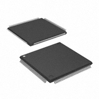


 工商网监
湘ICP备2023018690号
工商网监
湘ICP备2023018690号
