TMUX136
TMUX136
SCDS367D – AUGUST 2017 – REVISED AUGUST
2020
SCDS367D – AUGUST 2017 – REVISED AUGUST 2020
www.ti.com
TMUX136 6-GHz, 2-Channel, 2:1 Switch, With Power-off Isolation
1 Features
3 Description
•
•
The TMUX136 device is a high performance, 6-GHz,
2-channel, 2:1 switch that will support both differential
and single ended signals. The device has a wide VCC
range of 2.3 V to 4.8 V and supports a power-off
protection feature forcing all I/O pins to be in highimpedance mode when power is not present on the
VCC pin. The select pins of TMUX136 are compatible
with 1.8-V control voltage, allowing them to be directly
interfaced with the General-Purpose I/O (GPIO) from
low voltage processors.
•
•
•
•
VCC Range 2.3 V to 4.8 V
High Performance Switch Characteristics:
– Bandwidth (–3 dB): 6.1 GHz
– RON (Typical): 5.7 Ω
– CON (Typical): 1.6 pF
Current Consumption: 30 µA (Typical)
Special Features:
– IOFF Protection Prevents Current Leakage in
Powered-Down State
– 1.8-V Compatible Control Inputs (SEL, EN)
ESD Performance:
– 5-kV Human Body Model (A114B, Class II)
– 1-kV Charged-Device Model (C101)
Compact 10-Pin UQFN Package
(1.5-mm × 2-mm, 0.5-mm Pitch)
2 Applications
•
•
•
•
•
•
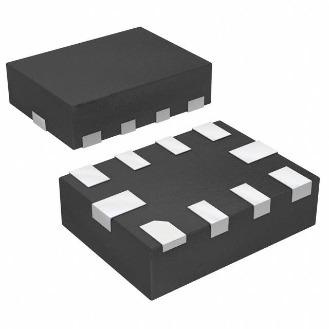
The TMUX136 comes in a small 10-pin UQFN
package with only 1.5 mm × 2 mm in size, which
makes it useful when PCB area is limited.
Device Information
PART NUMBER (1)
TMUX136
(1)
Handset: Smartphone
Notebook PC
Tablet: Multimedia
Electronic point of Sale
Field instrumentation
Portable Monitor
COM1
A1
COM2
A2
PACKAGE
UQFN (10)
BODY SIZE (NOM)
1.50 mm × 2.00 mm
For all available packages, see the orderable addendum at
the end of the data sheet.
A
B
VCC
B1
B2
Charge
Pump
Digital Control
SEL
EN
Simplified Schematic
EN (see Note A)
Note A: EN is the internal enable signal applied to the switch.
Functional Block Diagram
An IMPORTANT NOTICE at the end of this data sheet addresses availability, warranty, changes, use in safety-critical applications,
Submit Document Feedback
Copyright
© 2020 Texas
Instruments
Incorporated
intellectual
property
matters
and other important disclaimers. PRODUCTION DATA.
Product Folder Links: TMUX136
1
�TMUX136
www.ti.com
SCDS367D – AUGUST 2017 – REVISED AUGUST 2020
Table of Contents
1 Features............................................................................1
2 Applications..................................................................... 1
3 Description.......................................................................1
4 Revision History.............................................................. 2
5 Pin Configuration and Functions...................................3
Pin Functions.................................................................... 3
6 Specifications.................................................................. 4
6.1 Absolute Maximum Ratings........................................ 4
6.2 ESD Ratings............................................................... 4
6.3 Recommended Operating Conditions.........................4
6.4 Thermal Information....................................................5
6.5 Electrical Characteristics.............................................5
6.6 Dynamic Characteristics............................................. 7
6.7 Timing Requirements.................................................. 7
6.8 Typical Characteristics................................................ 8
7 Parameter Measurement Information............................ 9
8 Detailed Description...................................................... 11
8.1 Overview................................................................... 11
8.2 Functional Block Diagram......................................... 11
8.3 Feature Description...................................................11
8.4 Device Functional Modes..........................................11
9 Application and Implementation.................................. 12
9.1 Application Information............................................. 12
9.2 Typical Application.................................................... 12
10 Power Supply Recommendations..............................16
11 Layout........................................................................... 16
11.1 Layout Guidelines................................................... 16
11.2 Layout Example...................................................... 17
12 Device and Documentation Support..........................18
12.1 Documentation Support.......................................... 18
12.2 Receiving Notification of Documentation Updates..18
12.3 Support Resources................................................. 18
12.4 Trademarks............................................................. 18
12.5 Electrostatic Discharge Caution..............................18
12.6 Glossary..................................................................18
13 Mechanical, Packaging, and Orderable
Information.................................................................... 18
4 Revision History
Changes from Revision C (July 2018) to Revision D (August 2020)
Page
• Added new specification limits to support added temperature range TA = -40°C to +125°C .............................4
Changes from Revision B (November 2017) to Revision C (July 2018)
Page
• Changed pin 6 To: EN, pin 7 To: COM2, and pin 8 To: COM1 in Figure 11-2 ..................................................17
Changes from Revision A (October 2017) to Revision B (November 2017)
Page
• Changed Pin 7 From: COM1 To: COM2............................................................................................................. 3
• Changed Pin 8 From: COM2 To: COM1............................................................................................................. 3
Changes from Revision * (August 2017) to Revision A (October 2017)
Page
• Changed the HBM value From: ±3500 To: ±5000 in the ESD Ratings table...................................................... 4
2
Submit Document Feedback
Copyright © 2020 Texas Instruments Incorporated
Product Folder Links: TMUX136
�TMUX136
www.ti.com
SCDS367D – AUGUST 2017 – REVISED AUGUST 2020
10
VCC
5 Pin Configuration and Functions
1
9
SEL
A2
2
8
COM1
B1
3
7
COM2
B2
4
6
EN
GND
5
A1
Not to scale
Figure 5-1. RSE Package 10 Pin (UQFN) Top View
Pin Functions
PIN
NO.
NAME
I/O
DESCRIPTION
1
A1
I/O
Signal path A1
2
A2
I/O
Signal path A2
3
B1
I/O
Signal path B1
4
B2
I/O
Signal path B2
5
GND
—
Ground
6
EN
I
7
COM2
I/O
Enable (Active Low)
Common signal path 2
8
COM1
I/O
Common signal path 1
9
SEL
I
10
VCC
—
Switch select (logic Low = COM to A PORT Logic High = COM to B PORT)
Supply Voltage
Submit Document Feedback
Copyright © 2020 Texas Instruments Incorporated
Product Folder Links: TMUX136
3
�TMUX136
www.ti.com
SCDS367D – AUGUST 2017 – REVISED AUGUST 2020
6 Specifications
6.1 Absolute Maximum Ratings
over operating free-air temperature range (unless otherwise noted)(1) (2)
Supply voltage(3)
VCC
voltage(3)
MIN
MAX
UNIT
–0.3
5.5
V
–0.3
5.5
V
–0.3
5.5
V
VI/O
Input-output DC
VSEL, V EN
Digital input voltage (SEL, EN)
IK
Input-output port diode current
VI/O < 0
–50
mA
IIK
Digital logic input clamp current(3)
VI < 0
–50
mA
ICC
Continuous current through VCC
IGND
Continuous current through GND
–100
Tstg
Storage temperature
–65
(1)
(2)
(3)
100
mA
mA
150
°C
Stresses beyond those listed under Absolute Maximum Ratings may cause permanent damage to the device. These are stress ratings
only, which do not imply functional operation of the device at these or any other conditions beyond those indicated under
Recommended Operating Conditions. Exposure to absolute-maximum-rated conditions for extended periods may affect device
reliability.
The algebraic convention, whereby the most negative value is a minimum and the most positive value is a maximum.
All voltages are with respect to ground, unless otherwise specified.
6.2 ESD Ratings
VALUE
V(ESD)
(1)
(2)
Electrostatic
discharge
Human body model (HBM), per ANSI/ESDA/JEDEC JS-001(1)
±5000
Charged-device model (CDM), per JEDEC specification JESD22-C101(2)
±1000
UNIT
V
JEDEC document JEP155 states that 500-V HBM allows safe manufacturing with a standard ESD control process.
JEDEC document JEP157 states that 250-V CDM allows safe manufacturing with a standard ESD control process.
6.3 Recommended Operating Conditions
4
MIN
MAX
VCC
Supply voltage
2.3
4.8
V
VI/O
Analog voltage
0
3.6
V
VSEL, V EN
Digital input voltage (SEL, EN)
0
VCC
V
TRAMP (VCC)
Power supply ramp time requirement (VCC)
100
1000
μs/V
II/O
Continous current through I/O signal path (COMx, Ax, Bx) TA = –40°C to +85°C
±20
mA
II/O
Continous current through I/O signal path (COMx, Ax, Bx) TA = –40°C to +125°C
±10
mA
TA
Operating free-air temperature
125
°C
–40
Submit Document Feedback
UNIT
Copyright © 2020 Texas Instruments Incorporated
Product Folder Links: TMUX136
�TMUX136
www.ti.com
SCDS367D – AUGUST 2017 – REVISED AUGUST 2020
6.4 Thermal Information
TMUX136
THERMAL METRIC
(1)
RSE (UQFN)
UNIT
10 PINS
RθJA
Junction-to-ambient thermal resistance
191.6
°C/W
RθJC(top)
Junction-to-case (top) thermal resistance
94.3
°C/W
RθJB
Junction-to-board thermal resistance
117.5
°C/W
ψJT
Junction-to-top characterization parameter
7.4
°C/W
ψJB
Junction-to-board characterization parameter
117.4
°C/W
(1)
For more information about traditional and new thermal metrics, see the Semiconductor and IC Package Thermal Metrics application
report.
6.5 Electrical Characteristics
TA = –40°C to +85°C, Typical values are at VCC = 3.3 V, TA = 25°C, (unless otherwise noted)
PARAMETER
TEST CONDITIONS
MIN
TYP MAX
UNIT
A PORT SWITCH
RON
ΔRON
RON
(FLAT)
IOZ
IOFF
VCC = 2.7 V
VI/O = 1.65 V, ION = –8 mA
5.7
9
5.7
9.5
VCC = 2.3 V
VI/O = 1.65 V, ION = –8 mA
VCC = 2.7 V
VI/O = 1.65 V, ION = –8 mA
TA = –40°C to +125°C
13
VCC = 2.3 V
VI/O = 1.65 V, ION = –8 mA
TA = –40°C to +125°C
13
ON-state resistance
match between signal
path 1 and 2
VCC = 2.3 V
VI/O = 1.65 V, ION = –8 mA
ON-state resistance
flatness
VCC = 2.3 V
VI/O = 1.65 V to 3.45 V, ION = –8 mA
ON-state resistance
OFF leakage current
Power-off leakage
current
VCC = 4.8 V
VCC = 0 V
VCC = 4.8 V
ION
ON leakage current
VCC = 2.3 V
Ω
0.1
Ω
1
Ω
Switch OFF, VB = 1.65 V to 3.45 V,
VCOM = 0 V
–2
2
Switch OFF, VB = 1.65 V to 3.45 V,
VCOM = 0 V
TA = –40°C to +125°C
–15
15
Switch ON or OFF, VB = 1.65 V to 3.45 V,
VCOM = NC
–10
10
Switch ON or OFF, VB = 1.65 V to 3.45 V,
VCOM = NC
TA = –40°C to +125°C
–50
50
Switch ON, VB = 1.65 V to 3.45 V,
VCOM = NC
–2
2
Switch ON, VB = 1.65 V to 3.45 V,
VCOM = NC
TA = –40°C to +125°C
–15
15
Switch ON, VB = 1.65 V to 3.45 V,
VCOM = NC
–125
125
Switch ON, VB = 1.65 V to 3.45 V,
VCOM = NC
TA = –40°C to +125°C
–175
175
µA
µA
µA
B PORT SWITCH
VI/O = 0.4 V, ION = –8 mA
RON
ON-state resistance
VCC = 2.3 V
VI/O = 0.4 V, ION = –8 mA
TA = –40°C to +125°C
4.6
7.5
12
Ω
Submit Document Feedback
Copyright © 2020 Texas Instruments Incorporated
Product Folder Links: TMUX136
5
�TMUX136
www.ti.com
SCDS367D – AUGUST 2017 – REVISED AUGUST 2020
TA = –40°C to +85°C, Typical values are at VCC = 3.3 V, TA = 25°C, (unless otherwise noted)
PARAMETER
TEST CONDITIONS
ON-state resistance
match between signal
path 1 and 2
VCC = 2.3 V
VI/O = 0.4 V, ION = –8 mA
(FLAT)
ON-state resistance
flatness
VCC = 2.3 V
VI/O = 0 V to 0.4 V, ION = –8 mA
IOZ
OFF leakage current
VCC = 4.8 V
ΔRON
RON
IOFF
Power-off leakage
current
VCC = 0 V
VCC = 4.8 V
VCC = 4.8 V
ION
ON leakage current
VCC = 2.3 V
VCC = 2.3 V
MIN
TYP MAX
UNIT
0.1
Ω
1
Ω
Switch OFF, VA = 0 V to 3.6 V, VCOM = 0 V
–2
2
Switch OFF, VA = 0 V to 3.6 V, VCOM = 0 V
TA = –40°C to +125°C
–15
15
Switch ON or OFF, VA = 0 V to 3.6 V,
VCOM = NC
–10
10
Switch ON or OFF, VA = 0 V to 3.6 V,
VCOM = NC
TA = –40°C to +125°C
–50
50
Switch ON, VA = 0 V to 3.6 V,
VD± = NC
–2
2
Switch ON, VA = 0 V to 3.6 V,
VD± = NC
TA = –40°C to +125°C
–15
15
Switch ON, VA = 0 V to 3.6 V,
VB = NC
–125
125
Switch ON, VA = 0 V to 3.6 V,
VB = NC
TA = –40°C to +125°C
–175
175
µA
µA
µA
DIGITAL CONTROL INPUTS (SEL, EN)
6
VIH
Input logic high
VCC = 2.3 V to 4.8 V
TA = –40°C to +125°C
VIL
Input logic low
VCC = 2.3 V to 4.8 V
TA = –40°C to +125°C
IIN
Input leakage current
VCC = 4.8 V, VI/O = 0 V to 3.6 V, VIN = 0 to 4.8 V
Submit Document Feedback
1.3
–10
V
0.6
V
10
μA
Copyright © 2020 Texas Instruments Incorporated
Product Folder Links: TMUX136
�TMUX136
www.ti.com
SCDS367D – AUGUST 2017 – REVISED AUGUST 2020
6.6 Dynamic Characteristics
over operating free-air temperature range (unless otherwise noted)
PARAMETER
TEST CONDITIONS
MIN
TYP
MAX
UNIT
PORT B ON capacitance
VCC = 3.3 V, VI/O = 0 or 3.3 V,
f = 240 MHz
Switch ON
1.6
2
pF
PORT A ON capacitance
VCC = 3.3 V, VI/O = 0 or 3.3 V,
f = 240 MHz
Switch ON
1.4
2
pF
PORT B OFF capacitance
VCC = 3.3 V, VI/O = 0 or 3.3 V
f = 240 MHz
Switch OFF
1.4
2
pF
PORT A OFF capacitance
VCC = 3.3 V, VI/O = 0 or 3.3 V
f = 240 MHz
Switch OFF
1.6
2
pF
CI
Digital input capacitance
VCC = 3.3 V, VI = 0 or 2 V
OISO
OFF Isolation
VCC = 2.3 V to 4.8 V, RL = 50 Ω,
f = 240 MHz
XTALK
Crosstalk
BW
–3-dB bandwidth
CON
COFF
2.2
pF
Switch OFF
–34
dB
VCC = 2.3 V to 4.8 V, RL = 50 Ω,
f = 240 MHz
Switch ON
–37
dB
VCC = 2.3 V to 4.8 V, RL = 50 Ω,
Switch ON
6.1
GHz
SUPPLY
VCC
Power supply voltage
2.3
VCC = 4.8 V, VIN = VCC or GND, VI/O = 0 V,
Switch ON or OFF
ICC
Icc, HZ
Positive supply current
4.8
30
50
µA
VCC = 4.8 V, VIN = VCC or GND, VI/O = 0 V,
Switch ON or OFF
TA = –40°C to +125°C
Power supply current in high-Z
mode
V
70
VCC = 4.8 V, VIN = VCC or GND, VI/O = 0 V,
Switch ON or OFF, OE = H
5
10
µA
VCC = 4.8 V, VIN = VCC or GND, VI/O = 0 V,
Switch ON or OFF, OE = H
TA = –40°C to +125°C
20
6.7 Timing Requirements
MIN
tpd
Propagation delay
tswitch
Switching time (SEL to output)
tZH, ZL
Enable time ( EN to output)
tHZ, LZ
Disable time ( EN to output)
tSK(P)
Skew of opposite transitions of same output
VI/O = 3.3 V or 0 V
RL = 50 Ω,
CL = 5 pF,
VCC = 2.3 V to 4.8 V
NOM
MAX
100
ps
600
100
UNIT
ns
µs
200
ns
20
ps
Submit Document Feedback
Copyright © 2020 Texas Instruments Incorporated
Product Folder Links: TMUX136
7
�TMUX136
www.ti.com
SCDS367D – AUGUST 2017 – REVISED AUGUST 2020
6.8 Typical Characteristics
6.0
5.5
Ron (Ÿ)
5.0
4.5
4.0
3.5
3.0
2.5
2.0
0.0
0.4
0.8
1.2
1.6
2.0
2.4
2.8
3.2
Vin (V)
3.6
4.0
C002
Figure 6-1. ON-Resistance vs VI/O
Figure 6-3. Off Isolation
8
Figure 6-2. Bandwidth
Figure 6-4. Cross Talk
Submit Document Feedback
Copyright © 2020 Texas Instruments Incorporated
Product Folder Links: TMUX136
�TMUX136
www.ti.com
SCDS367D – AUGUST 2017 – REVISED AUGUST 2020
7 Parameter Measurement Information
A
COM
3V
1.8 V
B
CL
RL
VSEL
50 %
50 %
0V
SEL
CL
RL
tSWITCH
3V
VA/B
VSEL
tSWITCH
50 %
50 %
0V
Copyright © 2017, Texas Instruments Incorporated
A. All input pulses are suppleid by generators having the following characteristics: PRR ≤ 10 MHz, ZO = 50 Ω , tr < 5 ns, tf < 5 ns.
B. CL includes probe and jig capacitance.
Figure 7-1. Timing Diagram
VDD
VOUT1
VON
VOUT2
+
Channel ON
SEL
ION
VSEL
+
RON = (VON – VI/O1) / ION or (VON –
VI/O2) / ION
VSEL = H or L
GND
Figure 7-2. ON-State Resistance (RON)
VDD
VOUT1
VOUT2
+
A
SEL
Channel OFF
+
VSEL
IOZ
VIN
VSEL = H or L
+
GND
Figure 7-3. OFF Leakage Current (IOZ)
Submit Document Feedback
Copyright © 2020 Texas Instruments Incorporated
Product Folder Links: TMUX136
9
�TMUX136
www.ti.com
SCDS367D – AUGUST 2017 – REVISED AUGUST 2020
VDD
Network Analyzer
VOUT+
RS
VS
VOUT-
RS
Channel ON
VS
VSEL = H or L
RS=RL=50Ω
GND
RL
RL
Figure 7-4. Bandwidth (BW)
10
Submit Document Feedback
Copyright © 2020 Texas Instruments Incorporated
Product Folder Links: TMUX136
�TMUX136
www.ti.com
SCDS367D – AUGUST 2017 – REVISED AUGUST 2020
8 Detailed Description
8.1 Overview
The TMUX136 device is a 2-channel, 2:1, switch specifically designed for the switching of high-speed signals in
handset and consumer applications, such as cell phones, tablets, and notebooks but may be used for any high
speed application. The wide bandwidth (6.1 GHz) of this switch allows signals to pass with minimum edge and
phase distortion. The switch is bidirectional and offers little or no attenuation of the high-speed signals at the
outputs and will support both signle-ended and differential signals. The device also has a low power mode that
reduces the power consumption to 5 μA for portable applications with a battery or limited power budget.
The TMUX136 device integrates ESD protection cells on all pins, is available in a tiny UQFN package
(1.5 mm × 2 mm) and is characterized over the free-air temperature range from –40°C to +125°C.
8.2 Functional Block Diagram
A
B
VCC
Charge
Pump
EN (see Note A)
Note A: EN is the internal enable signal applied to the switch.
8.3 Feature Description
8.3.1 Low Power Mode
The TMUX136 has a low power mode that reduces the power consumption to 5 μA while the device is not in
use. To put the device in low power mode and disable the switch, the bus-switch enable pin EN must be supplied
with a logic High signal.
8.4 Device Functional Modes
8.4.1 High Impedance Mode
The TMUX136 has a high impedance mode that places all the signal paths in a Hi-Z state while the device is not
in use. To put the device in high impedance mode and disable the switch, the bus-switch enable pin EN must be
supplied with a logic High signal as shown in Table 8-1.
Table 8-1. Function Table
SEL
EN
SWITCH STATUS
X
High
Both A PORT and B PORT switches in High-Z
Low
Low
COM to A PORT
High
Low
COM to B PORT
Submit Document Feedback
Copyright © 2020 Texas Instruments Incorporated
Product Folder Links: TMUX136
11
�TMUX136
www.ti.com
SCDS367D – AUGUST 2017 – REVISED AUGUST 2020
9 Application and Implementation
Note
Information in the following applications sections is not part of the TI component specification, and TI
does not warrant its accuracy or completeness. TI’s customers are responsible for determining
suitability of components for their purposes. Customers should validate and test their design
implementation to confirm system functionality.
9.1 Application Information
9.2 Typical Application
There are many applications in which microprocessors or controllers have a limited number of I/Os. The
TMUX136 solution can effectively expand the limited I/Os by switching between multiple buses in order to
interface them to a single microprocessor or controller.
3.3 V
0.1 μF
VCC
System
Controller
Switch
Control Logic
2-channel
SPDT
SEL
OE
A1
A2
Port A
B1
B2
Port B
COM1
High Speed
Port
COM2
GND
Figure 9-1. Typical Application
9.2.1 Design Requirements
The TMUX136 has internal 6-MΩ pulldown resistors on SEL and EN, so no external resistors are required on the
logic pins. The internal pulldown resistor on SEL ensures PORT A channel is selected by default. The internal
pulldown resistor on EN enables the switch when power is applied to VCC.
9.2.1.1 Detailed Design Procedure
The TMUX136 can operate without any external components; however, TI recommends that unused pins must
be connected to ground through a 50-Ω resistor to prevent signal reflections back into the device.
12
Submit Document Feedback
Copyright © 2020 Texas Instruments Incorporated
Product Folder Links: TMUX136
�TMUX136
www.ti.com
SCDS367D – AUGUST 2017 – REVISED AUGUST 2020
9.2.2 Application Curves
Figure 9-2. Eye Pattern: 0.7 Gbps with No Device
Figure 9-3. Time Interval Error Histogram: 0.7 Gbps
with No Device
With Switch
The TMUX136 contributes only 8.4 ps of peak-to-peak jitter for
0.7-Gbps data rate
Figure 9-4. Eye Pattern: 0.7 Gbps with Switch
Figure 9-6. Eye Pattern: 2.2 Gbps with No Device
The TMUX136 contributes only 8.4 ps of peak-to-peak jitter for
0.7-Gbps data rate
Figure 9-5. Time Interval Error Histogram: 0.7 Gbps
with Switch
Figure 9-7. Time Interval Error Histogram: 2.2 Gbps
with No Device
Submit Document Feedback
Copyright © 2020 Texas Instruments Incorporated
Product Folder Links: TMUX136
13
�TMUX136
www.ti.com
SCDS367D – AUGUST 2017 – REVISED AUGUST 2020
With Switch
The TMUX136 contributes only 3.8 ps of peak-to-peak jitter for
2.2-Gbps data rate
Figure 9-8. Eye Pattern: 2.2 Gbps with Switch
Figure 9-10. Eye Pattern: 3 Gbps with No Device
The TMUX136 contributes only 3.8 ps of peak-to-peak jitter for
2.2-Gbps data rate
Figure 9-9. Time Interval Error Histogram: 2.2 Gbps
with Switch
Figure 9-11. Time Interval Error Histogram: 3 Gbps
with No Device
With Switch
The TMUX136 contributes only 5.8 ps of peak-to-peak jitter for
3-Gbps data rate
Figure 9-12. Eye Pattern: 3 Gbps with Switch
14
The TMUX136 contributes only 5.8 ps of peak-to-peak jitter for
3-Gbps data rate
Figure 9-13. Time Interval Error Histogram: 3 Gbps
with Switch
Submit Document Feedback
Copyright © 2020 Texas Instruments Incorporated
Product Folder Links: TMUX136
�TMUX136
www.ti.com
SCDS367D – AUGUST 2017 – REVISED AUGUST 2020
Figure 9-14. Eye Pattern: 4.5 Gbps with No Device
Figure 9-15. Time Interval Error Histogram: 4.5
Gbps with No Device
With Switch
The TMUX136 contributes only 7.6 ps of peak-to-peak jitter for
4.5-Gbps data rate
Figure 9-16. Eye Pattern: 4.5 Gbps with Switch
The TMUX136 contributes only 7.6 ps of peak-to-peak jitter for
4.5-Gbps data rate
Figure 9-17. Time Interval Error Histogram: 4.5
Gbps with Switch
Submit Document Feedback
Copyright © 2020 Texas Instruments Incorporated
Product Folder Links: TMUX136
15
�TMUX136
www.ti.com
SCDS367D – AUGUST 2017 – REVISED AUGUST 2020
10 Power Supply Recommendations
TI recommends placing a bypass capacitor as close to the supply pin VCC as possible to help smooth out lower
frequency noise to provide better load regulation across the frequency spectrum.
11 Layout
11.1 Layout Guidelines
Place supply bypass capacitors as close to VCC pin as possible and avoid placing the bypass caps near the
high speed traces.
The high-speed signalpaths must should be no more than 4 inches long; otherwise, the eye diagram
performance may be degraded.
Route the high-speed signals using a minimum of vias and corners which reduces signal reflections and
impedance changes. When a via must be used, increase the clearance size around it to minimize its
capacitance. Each via introduces discontinuities in the signal’s transmission line and increases the chance of
picking up interference from the other layers of the board. Be careful when designing test points on twisted pair
lines; through-hole pins are not recommended.
When it becomes necessary to turn 90°, use two 45° turns or an arc instead of making a single 90° turn. This
reduces reflections on the signal traces by minimizing impedance discontinuities.
Do not route high speed signal traces under or near crystals, oscillators, clock signal generators, switching
regulators, mounting holes, magnetic devices or ICs that use or duplicate clock signals.
Avoid stubs on the high-speed signals traces because they cause signal reflections. If a stub is unavoidable,
then the stub must be less than 200 mm.
Route all high-speed signal traces over continuous GND planes, with no interruptions.
Avoid crossing over anti-etch, commonly found with plane splits.
Due to high frequencies, a printed circuit board with at least four layers is recommended; two signal layers
separated by a ground and power layer as shown in Figure 11-1.
Signal 1
GND Plane
Power Plane
Signal 2
Figure 11-1. Four-Layer Board Stack-Up
The majority of signal traces must run on a single layer, preferably Signal 1. Immediately next to this layer must
be the GND plane, which is solid with no cuts. Avoid running signal traces across a split in the ground or power
plane. When running across split planes is unavoidable, sufficient decoupling must be used. Minimizing the
number of signal vias reduces EMI by reducing inductance at high frequencies.
16
Submit Document Feedback
Copyright © 2020 Texas Instruments Incorporated
Product Folder Links: TMUX136
�TMUX136
www.ti.com
SCDS367D – AUGUST 2017 – REVISED AUGUST 2020
11.2 Layout Example
LEGEND
VIA to Power Plane
Polygonal Copper Pour
VIA to GND Plane
Bypass Capacitor
V+
To Microcontroller
10
1 A1
VCC
SEL 9
Port A
2 A2
COM1 8
3 B1
COM2 7
To Common Port
Port B
4 B2
EN 6
GND
5
To Microcontroller
Figure 11-2. Package Layout Diagram
Submit Document Feedback
Copyright © 2020 Texas Instruments Incorporated
Product Folder Links: TMUX136
17
�TMUX136
www.ti.com
SCDS367D – AUGUST 2017 – REVISED AUGUST 2020
12 Device and Documentation Support
12.1 Documentation Support
12.1.1 Related Documentation
For related documentation see the following:
•
•
High-Speed Layout Guidelines Application Report
High-Speed Interface Layout Guidelines
12.2 Receiving Notification of Documentation Updates
To receive notification of documentation updates, navigate to the device product folder on ti.com. Click on
Subscribe to updates to register and receive a weekly digest of any product information that has changed. For
change details, review the revision history included in any revised document.
12.3 Support Resources
TI E2E™ support forums are an engineer's go-to source for fast, verified answers and design help — straight
from the experts. Search existing answers or ask your own question to get the quick design help you need.
Linked content is provided "AS IS" by the respective contributors. They do not constitute TI specifications and do
not necessarily reflect TI's views; see TI's Terms of Use.
12.4 Trademarks
TI E2E™ is a trademark of Texas Instruments.
All other trademarks are the property of their respective owners.
12.5 Electrostatic Discharge Caution
This integrated circuit can be damaged by ESD. Texas Instruments recommends that all integrated circuits be handled
with appropriate precautions. Failure to observe proper handling and installation procedures can cause damage.
ESD damage can range from subtle performance degradation to complete device failure. Precision integrated circuits may
be more susceptible to damage because very small parametric changes could cause the device not to meet its published
specifications.
12.6 Glossary
TI Glossary
This glossary lists and explains terms, acronyms, and definitions.
13 Mechanical, Packaging, and Orderable Information
The following pages include mechanical, packaging, and orderable information. This information is the most
current data available for the designated devices. This data is subject to change without notice and revision of
this document. For browser-based versions of this data sheet, refer to the left-hand navigation.
18
Submit Document Feedback
Copyright © 2020 Texas Instruments Incorporated
Product Folder Links: TMUX136
�PACKAGE OPTION ADDENDUM
www.ti.com
11-Dec-2021
PACKAGING INFORMATION
Orderable Device
Status
(1)
Package Type Package Pins Package
Drawing
Qty
Eco Plan
(2)
Lead finish/
Ball material
MSL Peak Temp
Op Temp (°C)
Device Marking
(3)
(4/5)
(6)
TMUX136MRSER
ACTIVE
UQFN
RSE
10
3000
RoHS & Green
NIPDAU
Level-1-260C-UNLIM
-40 to 125
19H
TMUX136RSER
ACTIVE
UQFN
RSE
10
3000
RoHS & Green
NIPDAU
Level-1-260C-UNLIM
-40 to 125
19G
(1)
The marketing status values are defined as follows:
ACTIVE: Product device recommended for new designs.
LIFEBUY: TI has announced that the device will be discontinued, and a lifetime-buy period is in effect.
NRND: Not recommended for new designs. Device is in production to support existing customers, but TI does not recommend using this part in a new design.
PREVIEW: Device has been announced but is not in production. Samples may or may not be available.
OBSOLETE: TI has discontinued the production of the device.
(2)
RoHS: TI defines "RoHS" to mean semiconductor products that are compliant with the current EU RoHS requirements for all 10 RoHS substances, including the requirement that RoHS substance
do not exceed 0.1% by weight in homogeneous materials. Where designed to be soldered at high temperatures, "RoHS" products are suitable for use in specified lead-free processes. TI may
reference these types of products as "Pb-Free".
RoHS Exempt: TI defines "RoHS Exempt" to mean products that contain lead but are compliant with EU RoHS pursuant to a specific EU RoHS exemption.
Green: TI defines "Green" to mean the content of Chlorine (Cl) and Bromine (Br) based flame retardants meet JS709B low halogen requirements of