����������
���
���
��� �������� ��
��������
�
��
SLLS367D − JUNE 1999 − REVISED AUGUST 2007
D 1.25 Gigabits Per Second (Gbps) Gigabit
D
D
D
D
Ethernet Transceiver
Based on the P802.3Z Specification
Transmits Serial Data up to 1.25 Gbps
Operates With 3.3-V Supply Voltage
5-V Tolerant on TTL Inputs
D Interfaces to Electrical Cables/Backplane or
D
D
D
D
Optical Modules
PECL Voltage Differential Signaling Load,
1 V Typ With 50 Ω − 75 Ω
Receiver Differential Input Voltage
200 mV Minimum
Low Power Consumption
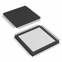
64-Pin Quad Flat Pack With Thermally
Enhanced Package
description
The TNETE2201B gigabit Ethernet transceiver provides for ultra high-speed bidirectional point-to-point data
transmission. This device is based on the timing requirements of the proposed 10-bit interface specification by
the P802.3z Gigabit Task Force.
1
64 63 62 61 60 59 58 57 56 55 54 53 52 51 50 49
48
2
47
3
46
4
45
5
44
6
43
7
42
8
41
9
40
10
39
11
38
12
37
13
36
14
35
15
34
33
16
1718 19 20 21 22 23 24 25 26 27 28 29 30 31 32
RC0
SYNC
GND_TTL
RD0
RD1
RD2
VCC_TTL
RD3
RD4
RD5
RD6
VCC_TTL
RD7
RD8
RD9
GND_TTL
TC0
VCC _TX
LOOPEN
VCC _A
GND_A
REFCLK
VCC _CMOS
SYNCEN
GND_CMOS
RESERVED
LCKREFN
VCC _A
VCC _A
RBC1
RBC0
GND_A
GND_CMOS
TD0
TD1
TD2
VCC_CMOS
TD3
TD4
TD5
TD6
VCC_CMOS
TD7
TD8
TD9
GND_CMOS
GND_TX
TC1
VCC _RX
RC1
GND_A
VCC _A
DOUT_TXP
DOUT_TXN
VCC _A
VCC _A
GND_CMOS
VCC _A
GND_A
VCC _A
DIN_RXP
VCC _A
DIN_RXN
GND_RX
PHD, PJD, OR PJW PACKAGE
(TOP VIEW)
Please be aware that an important notice concerning availability, standard warranty, and use in critical applications of
Texas Instruments semiconductor products and disclaimers thereto appears at the end of this data sheet.
Copyright 1999 − 2007, Texas Instruments Incorporated
���������� �
�
����������� �! "#��$�� �! �� %#&'�"����� (��$�)
���(#"�! "������ �� !%$"���"�����! %$� �*$ �$��! �� �$+�! ��!��#�$��!
!���(��( ,������-� ���(#"���� %��"$!!��. (�$! ��� �$"$!!���'- ��"'#($
�$!���. �� �'' %����$�$�!�
POST OFFICE BOX 655303
• DALLAS, TEXAS 75265
1
�����������
���
���
��� �������� ��
��������
�
�
SLLS367D − JUNE 1999 − REVISED AUGUST 2007
description (continued)
The intended application of this device is to provide building blocks for developing point-to-point baseband data
transmission over controlled-impedance media of approximately 50 Ω to 75 Ω. The transmission media can be
printed-circuit board traces, back planes, cables, or fiber optical media. The ultimate rate and distance of data
transfer is dependent upon the attenuation characteristics of the media and the noise coupling to the
environment.
The TNETE2201B performs the data serialization and deserialization (SERDES) functions for the gigabit
ethernet physical layer interface. The transceiver operates at 1.25 Gbps (typical), providing up to 1000 Mbps
of bandwidth over a copper or optical media interface. The serializer/transmitter accepts 8b/10b parallel
encoded data bytes. The parallel data bytes are serialized and transmitted differentially nonreturn-to-zero
(NRZ) at pseudo-ECL (PECL) voltage levels. The deserializer/receiver extracts clock information from the input
serial stream and deserializes the data, outputting a parallel 10-bit data byte. The 10-bit data bytes are output
with respect to two receive byte clocks (RBC0, RBC1), allowing a protocol device to clock the parallel bytes in
RBC clock rising edges.
The transceiver automatically locks onto incoming data without the need to prelock. However, the transceiver
can be commanded to lock to the externally supplied reference clock (REFCLK) as a reset function, if needed.
The TNETE2201B provides an internal loopback capability for self-test purposes. Serial data from the serializer
is passed directly to the deserializer allowing the protocol device a functional self-check of the physical interface.
The TNETE2201B is characterized for operation from 0°C to 70°C.
2
POST OFFICE BOX 655303
• DALLAS, TEXAS 75265
�����������
���
���
��� �������� ��
��������
�
�
SLLS367D − JUNE 1999 − REVISED AUGUST 2007
functional block diagram
LOOPEN
TX+
TX−
TD0 − TD9
10
/
10-Bit
Register
10
/
Clock
Multiplier
REFCLK
125 MHz
SYNCEN
Synchronous
Detect
SYNC
RD0 − RD9
Shift
Register
10
/
10-Bit
Register
10
/
Shift
Register
62.5 MHz
RBC0
÷2
RBC1
125 MHz
PLL Clock
Recovery and
Data Retiming
62.5 MHz
2:1
MUX
RX+
RX−
POST OFFICE BOX 655303
• DALLAS, TEXAS 75265
3
�����������
���
���
��� �������� ��
��������
�
�
SLLS367D − JUNE 1999 − REVISED AUGUST 2007
I/O structures
PECL inputs (DIN_RXP, DIN_RXN)
PECL outputs (DIN_TXP, DIN_TXN)
VDD
VDD
100 Ω
DIN_RXP
DOUT_TXP
4 kΩ
VCM
VDD
+
_
VDD
4 kΩ
DIN_RXN
DOUT_TXN
CMOS inputs (TD0 − TD9, LOOPEN, REFCLK, SYNCEN, LCKREFN)
VDD
VDD
TERMINALS
P
R1
120 Ω
Input
Open Circuit Open Circuit
LOOPEN
Open Circuit
400 kΩ
400 kΩ
Open Circuit
N
CMOS outputs (RD0 − RD9, RBC0, RBC1, SYNC)
VDD
P
Output
N
4
POST OFFICE BOX 655303
R2
REFCLK, TD0 − TD9
SYNCEN, LCKREFN
R2
R1
• DALLAS, TEXAS 75265
�����������
���
���
��� �������� ��
��������
�
�
SLLS367D − JUNE 1999 − REVISED AUGUST 2007
Terminal Functions
TERMINAL
NAME
NO.
DESCRIPTION
TYPE
I/O and DATA
DOUT_TXP
DOUT_TXN
62
61
Output
Differential output transmit. DOUT_TXP and DOUT_TXN are differential serial outputs that interface
to a copper or an optical I/F module. These terminals transmit NRZ data at a rate of 1.25 Gbps.
DOUT_TXP and DOUT_TXN are held static when LOOPEN is high and are active when LOOPEN is
low.
DIN_RXP
DIN_RXN
54
52
Input
Differential input receive. DIN_RXP and DIN_RXN together are the differential serial input interface
from a copper or an optical I/F module. These terminals receive NRZ data at a rate of 1.25 Gbps and
are active when LOOPEN is held low.
LCKREFN
27
Input
Lock to reference. When LCKREFN is asserted low, the receive PLL phase locks to the supplied
REFCLK signal. LCKREFN prelocks or resets the receive PLL.
LOOPEN
19
Input
Loop enable. When LOOPEN is high (active), the internal loop-back path is activated. The
transmitted serial data is directly routed to the inputs of the receiver. This provides a self-test
capability in conjunction with the protocol device. The DOUT_TXP and DOUT_TXN outputs are held
static during the loop-back test. LOOPEN is held low during standard operational state with external
serial outputs and inputs active.
RBC0
RBC1
31
30
Output
Receive byte clock. RBC0 and RBC1 are 62.5-MHz recovered clocks used for synchronizing the
10-bit output data on RD0 − RD9. The 10-bit output data words are valid on the rising edges of RBC0
and RBC1. These clocks are adjusted to half-word boundaries in conjunction with synchronous
detect. The clocks are always expanded during data realignment and never slivered or truncated.
RBC0 registers bytes 1 and 3 of received data. RBC1 registers bytes 0 and 2 of received data.
RC1,
RC0
49
48
Analog
Receive capacitor. RC0 and RC1 are external capacitor connections used for the receiver internal
PLL filter. The recommend value for this external capacitor is 2 nF (a value of 0.1 µF can also be used,
see Note 1).
45,44,43,41
40,39,38,36
35,34
Output
Receive data. These outputs carry 10-bit parallel data output from the transceiver to the protocol
layer. The data is referenced to terminals RBC0 and RBC1. Received data byte 0, which contains the
K28.5 character, is byte aligned to the rising edge of RBC1. RD0 is the first bit received.
REFCLK
22
Input
Reference clock. REFCLK is an external 125 MHz input clock that synchronizes the receiver and
transmitter interfaces. The transmitter uses this clock to register the 10-bit input data (TD0..TD9) for
serialization. REFCLK is also used as a RX PLL preset or reference when LCKREFN is enabled.
SYNC
47
Output
Synchronous detect. SYNC is asserted high upon detection of the K28.5 character in the serial data
path. SYNC is a high level for 1/2 REFCLK period. SYNC pulses are output only when SYNCEN is
activated (asserted high). Note: SYNC is active on byte0 and, therefore, active on rising edge of
RCB1.
SYNCEN
24
Input
Synchronous function enable. When SYNCEN is asserted high, the internal synchronization function
is activated. When this function is enabled, the transceiver detects the K28.5 character (0011111010
negative beginning disparity) in the serial data stream and realigns data on byte boundaries if
required. When SYNCEN is low, serial input data is unframed in RD0 − RD9.
TC1
TC0
16
17
Analog
Transmit capacitor. TC0 and TC1 are external capacitor connections used for the transmitter internal
PLL filter. The recommended value of this external capacitor is 2 nF (a value of 0.1 µF can also be
used, see Note 1).
2,3,4,6
7,8,9,11
12,13
Input
Transmit data. These inputs carry 10-bit parallel data output from a protocol device to the transceiver
for serialization and transmission. This 10-bit parallel data is clocked into the transceiver on the rising
edge of REFCLK and transmitted as a serial stream with TD0 sent as the first bit.
RD0 − RD9
TD0 − TD9
NOTE 1: A filter capacitor value of 0.1 µF can be used with the following consideration: The tracking bandwidth of the PLL will be reduced due
to the larger filter capacitor. This reduces the transmit and receive PLL’s ability to reject low-frequency noise or wonder in the voltage
supply or datastream. Care must be taken in the filtering of the supply VCC_TX (terminal 18) and VCC_RX (terminal 50) to reject power
supply noise.
POST OFFICE BOX 655303
• DALLAS, TEXAS 75265
5
�����������
���
���
��� �������� ��
��������
�
�
SLLS367D − JUNE 1999 − REVISED AUGUST 2007
Terminal Functions (Continued)
TERMINAL
NAME
NO.
DESCRIPTION
TYPE
POWER
VCC_A
20,28,29,53
55,57,59,60
63
Supply
Analog power. VCC_A provides a supply reference voltage for the high-speed analog circuits.
5,10,23,
Supply
Digital PECL logic power. VCC_CMOS provides an isolated low-noise power supply for the logic
circuits.
VCC_RX
50
Supply
Receiver power. VCC_RX provides a low-noise supply reference voltage for the receiver high-speed
analog circuits.
VCC_TTL
VCC_TX
42,37
Supply
TTL power. VCC_TTL provides a supply reference voltage for the receiver TTL circuits.
18
Supply
Transmitter power. VCC_TX provides a low-noise supply reference voltage for the transmitter
high-speed analog circuits.
VCC_CMOS
GROUND
GND_A
21,32,56,64
Ground
Analog ground. GND_A provides a ground reference for the high-speed analog circuits.
1,14,
25,58
Ground
Digital PECL logic ground. GND_CMOS provides an isolated low-noise ground for the logic circuits.
GND_RX
51
Ground
Receiver ground. GND_RX provides a ground reference for the receiver circuits.
GND_TTL
33,46
Ground
TTL circuit ground. GND_TTL provides a ground for TTL interface circuits.
GND_TX
15
Ground
Transmitter ground. GND_TX provides a ground reference for the transmitter circuits.
RESERVED
26
GND_CMOS
MISCELLANEOUS
Reserved. Internally pulled to GND, leave open or assert low.
detailed description
data transmission
The transmitter registers incoming 10-bit-wide data words (8b/10b encoded data, TD0...TD9) on the rising edge
of REFCLK (125 MHz). The reference clock is also used by the serializer, which multiplies the clock by a factor
of 10 providing a 1.25 Gbaud signal that is fed to the shift register. The data is then transmitted differentially at
PECL voltage levels. The 8b/10b encoded data is transmitted sequentially bit 0 through 9.
transmission latency
The data transmission latency of the TNETE2201B is defined as the delay from the initial 10-bit word load to
the serial transmission of bit 9. The typical transmission latency is 9 ns.
data reception
The receiver of the TNETE2201B deserializes 1.25 Gbps differential serial data. The 8b/10b data (or equivalent)
is retimed based on an extracted clock from the serial data. The serial data is then aligned to the 10-bit word
boundaries and presented to the protocol controller along with two receive byte clocks (RBC0, RBC1). RBC0
and RBC1 are 180 degrees out of phase and are generated by dividing down the recovered 1.25 Gbps
(625 MHz) clock by 10 providing for two 62.5-MHz signals. The receiver presents the protocol device byte 0 of
the received data valid on the rising edge of RBC1.
NOTE:
This allows the option of byte alignment without the use of the synchronous detection
(SYNC) function by the protocol device.
The receiver PLL can lock to the incoming 1.25 GHz data without the need for a lock-to-reference preset. The
received serial data rate (RX+ and RX−) should be 1.25 Gbps ± 0.01% (100 ppm) for proper operation.
6
POST OFFICE BOX 655303
• DALLAS, TEXAS 75265
�����������
���
���
��� �������� ��
��������
�
�
SLLS367D − JUNE 1999 − REVISED AUGUST 2007
data reception (continued)
During a bus error condition or word alignment, the receive byte clocks RBC0 and RBC1 are stretched (never
truncated). When the incoming serial data does not meet its frequency requirements, then the receive byte clock
frequency is maintained at 62.5 MHz.
receive PLL operation
The receive PLL provides automatic locking to the incoming data. At power up, the maximum initial lock time
is 500 µs. The PLL can also be initiated or set to phase lock to the externally supplied reference clock by enabling
lock-to-reference (LCKREFN). The lock-to-reference causes the receive PLL to lock to 10× the reference clock
(REFCLK) input providing a PLL preset and reset capability.
If during normal operation a transient occurs, which is defined as any arbitrary phase shift in the incoming data
and/or a frequency wander of up to 200 ppm, then the PLL recovers lock within 2.4 µs. Any condition exceeding
these values is considered a power-up scenario and the PLL recovers lock within 500 µs with a 0.1 µF capacitor
the PLL recovers lock within 10 ms on power up (see the following note).
NOTE:
A filter capacitor value of 0.1 µF can be used with the following consideration: The tracking
bandwidth of the PLL will be reduced due to the larger filter capacitor. This reduces the transmit and
receive PLL’s ability to reject low-frequency noise or wonder in the voltage supply or datastream.
Care must be taken in the filtering of the supply VCC_TX (terminal 18) and VCC_RX (terminal 50)
to reject power supply noise.
receiver word alignment
The TNETE2201B uses a 10-bit K28.5 character (comma character) word alignment scheme. The following
sections explain how this scheme works and how it realigns itself.
comma character on expected boundary
The TNETE2201B provides 10-bit K28.5 character recognition and word alignment. The 10-bit word alignment
is enabled by forcing SYCNEN high. This enables the function that examines and compares ten bits of serial
input data to the K28.5 synchronization character. The K28.5 character is defined in the fibre channel standard
as a pattern consisting of 0011111010 (a negative number beginning disparity) with the 7 MSBs (0011111)
referred to as the comma character. The K28.5 character was implemented specifically for aligning data words.
As long as the K28.5 character falls within the expected 10-bit word boundary, the received 10-bit data is
properly aligned and data realignment is not required. Figure 1 shows the timing characteristics of RBC0, RBC1,
SYNC and RD0 − RD9 while synchronized.
NOTE:
The K28.5 character is valid on the rising edge of RBC1.
RBC0
RBC1
SYNC
RD0 − RD9
K28.5
Dxx.x
Dxx.x
Dxx.x
K28.5
Dxx.x
Figure 1. Synchronous Timing Characteristics Waveforms
POST OFFICE BOX 655303
• DALLAS, TEXAS 75265
7
�����������
���
���
��� �������� ��
��������
�
�
SLLS367D − JUNE 1999 − REVISED AUGUST 2007
comma character not on expected boundary
When synchronization is enabled and a K28.5 character straddles the expected 10-bit word boundary, then
word realignment is necessary. Realignment or shifting the 10-bit word boundary truncates the character
following the misaligned K28.5, but the following K28.5 and all subsequent data is aligned properly as shown
in Figure 2. The 10b specification requires that RCLK cycles can not be truncated and can only be stretched
or stalled in their current state during realignment. With this design the maximum stretch that occurs is an extra
10 bit times. This occurs during a worst case scenario when the K28.5 is aligned to the falling edge of RBC1
instead of the rising edge. This system transmits a minimum of three consecutively ordered K28.5 data sets
between frames and ensures that the receiver sees at least two of K28.5 sets (the fabric is allowed to drop one).
Figure 2 shows the timing characteristics of the data realignment.
Systems that do not require framed data can disable byte alignment by tying SYNCEN low.
When a synchronization character is detected the SYNC signal is asserted high and is aligned with the K28.5
character. The duration of the SYNC-signal pulse is equal to the duration of the data which is half an RCLK
period.
Typical Receive
Path Latency = 18 ns
Serial Rx Data Stream
DIN_RxP − DIN_RxN
K28.5
Dxx.x
Dxx.x
K28.5
Dxx.x
Dxx.x
Dxx.x
K28.5
Dxx.x
K28.5
Dxx.x
K28.5
10 Bit Times
10 Bit Times
20 Bit Times
(MAX)
RBC1
RBC0
Corrupted Data
Misalignment
Corrected
Worst Case
Misaligned K28.5
RD0 − RD9
Dxx.x
Dxx.x
K28.5
Dxx.x
Dxx.x
K28.5
Dxx.x
Dxx.x
SYNC
Figure 2. Word Realignment Timing Characteristics Waveforms
data reception latency
The serial-to-parallel data latency is the time from when the first bit arrives at the receiver until it is output in the
aligned parallel word with RD0 received as first bit. The receive latency is typically 18 ns.
8
POST OFFICE BOX 655303
• DALLAS, TEXAS 75265
�����������
���
���
��� �������� ��
��������
�
�
SLLS367D − JUNE 1999 − REVISED AUGUST 2007
loop-back testing
The transceiver can provide a self-test function by enabling (LOOPEN to high level) the internal loop-back path.
Enabling LOOPEN causes serially transmitted data to be routed internally to the receiver. The parallel data
output can be compared to the parallel input data for functional verification. The external differential output is
held in a static state during loop-back testing.
absolute maximum ratings†
Supply voltage, VCC (see Note 2) . . . . . . . . . . . . . . . . . . . . . . . . . . . . . . . . . . . . . . . . . . . . . . . . . . . . . −0.5 to 4.0 V
Input voltage, VI (TTL, PECL) . . . . . . . . . . . . . . . . . . . . . . . . . . . . . . . . . . . . . . . . . . . . . . . . . . . . . . . . −0.5 to 4.0 V
Output current IO, (TTL) . . . . . . . . . . . . . . . . . . . . . . . . . . . . . . . . . . . . . . . . . . . . . . . . . . . . . . . . . . . . . . . . . . 50 mA
Output current IO, (PECL) . . . . . . . . . . . . . . . . . . . . . . . . . . . . . . . . . . . . . . . . . . . . . . . . . . . . . . . . . . . . . . . . −50 mA
Voltage range at any terminal . . . . . . . . . . . . . . . . . . . . . . . . . . . . . . . . . . . . . . . . . . . . . . . . . . −0.5 to VCC + 0.5 V
Electrostatic discharge, 5-V tolerant input terminals (see Note 3) . . . . . . . . . . . . . . Class 1, A:1 kV, B:150 V
Electrostatic discharge, all other terminals (see Note 3) . . . . . . . . . . . . . . . . . . . . . . Class 1, A:2 kV, B:200 V
Characterized free-air operating temperature range . . . . . . . . . . . . . . . . . . . . . . . . . . . . . . . . . . . . . 0°C to 70°C
Storage temperature . . . . . . . . . . . . . . . . . . . . . . . . . . . . . . . . . . . . . . . . . . . . . . . . . . . . . . . . . . . . . −65°C to 150°C
† Stresses beyond those listed under “absolute maximum ratings” may cause permanent damage to the device. These are stress ratings only, and
functional operation of the device at these or any other conditions beyond those indicated under “recommended operating conditions” is not
implied. Exposure to absolute-maximum-rated conditions for extended periods may affect device reliability.
NOTES: 2. All voltage values, except differential I/O bus voltages, are with respect to network ground.
3. This parameter is tested in accordance with MIL-PRF-38535.
recommended operating conditions
PARAMETER
TEST CONDITIONS
Supply voltage, VCC
Supply current, ICC (static)
Static pattern†
Power dissipation, PD (static)
Outputs open,
Supply current, ICC (dynamic)
K28.5
Power dissipation, PD (dynamic)
Outputs open,
MIN
NOM
MAX
UNIT
3.14
3.3
3.47
V
180
260
mA
590
900
mW
Static pattern†
K28.5
Operating free-air temperature, TA
† Power (static pattern) = 125 MHz to the receiver and 5 ones and 5 zeros to the transmitter.
240
330
mA
790
1150
mW
0
70
°C
reference clock (REFCLK) timing requirements over recommended operating conditions (unless
otherwise noted)†
PARAMETER
TEST CONDITIONS
MIN
TYP −
0.01%
Frequency
Accuracy
−100
Duty cycle
40%
NOM
MAX
UNIT
125
TYP +
0.01%
MHz
100
ppm
50%
60%
Jitter
Random and deterministic
40
ps
† This clock should be crystal referenced to meet the requirements of the this table. The maximum rate of frequency change specified is valid after
10 seconds from power on.
POST OFFICE BOX 655303
• DALLAS, TEXAS 75265
9
�����������
���
���
��� �������� ��
��������
�
�
SLLS367D − JUNE 1999 − REVISED AUGUST 2007
electrical characteristics over recommended operating conditions (unless otherwise noted)
TTL Signals: TD0 .. TD9, REFCLK, LOOPEN, SYNCEN, SYNC, RD0 .. RD9, RBC0, RBC1, LCKREFN
PARAMETER
VOH
VOL
High-level output voltage
VIH
VIL
High-level input voltage
IIH
High-level input current
Low-level output voltage
IOH = − 400 µA
IOL = 1 mA
MIN
TYP
2.4
3
0.25
2
Low-level input voltage
IIL
Low-level input current
ci
Input capacitance
10
TEST CONDITIONS
VCC = MIN,
VCC = MIN,
REFCLK
VCC = MAX,
VCC = MAX,
VI = 2.4 V
VI = 2.4 V
REFCLK
VCC = MAX,
VCC = MAX,
VI = 0.4 V
VI = 0.4 V
MAX
V
0.4
V
5.5
V
0.8
V
40
µA
900
µA
µA
−40
µA
−900
4
POST OFFICE BOX 655303
• DALLAS, TEXAS 75265
UNIT
pF
�����������
���
���
��� �������� ��
��������
�
�
SLLS367D − JUNE 1999 − REVISED AUGUST 2007
TRANSMITTER SECTION
differential electrical characteristics over recommended operating conditions (unless otherwise
noted)
PARAMETER
TEST CONDITIONS
VODP
Driver differential output voltage (peak) (TXP − TXN )
RL = 75 Ω,
RL = 50 Ω,
VOC
Driver common-mode output voltage
RL = 75 Ω
MIN
TYP
MAX
See Figure 3
550
1100
See Figure 3
550
1100
2100
UNIT
mV
mV
differential switching characteristics over recommended operating conditions (unless otherwise
noted).
PARAMETER
tr3
tf3
TEST CONDITIONS
MIN
TYP
MAX
UNIT
Serial data deterministic jitter (peak-to-peak)
Differential output jitter
80
ps
Serial data total jitter (peak-to-peak)
Differential output jitter
192
ps
Differential signal rise time (20% to 80%)
RL = 75 Ω,,
See Figure 3
300
ps
300
ps
Differential signal fall time (20% to 80%)
CL = 5 pF,
80%
TX+
≈ VCC − 0.7 V
50%
20%
≈ VCC − 1.6 V
80%
≈ VCC − 0.7 V
tf
tr
TX−
50%
20%
≈ VCC − 1.6 V
tr
tf
80%
VOD
0V
20%
tr3
|VOD|P
tf3
Figure 3. Differential and Common-Mode Output Voltage Definitions
POST OFFICE BOX 655303
• DALLAS, TEXAS 75265
11
�����������
���
���
��� �������� ��
��������
�
�
SLLS367D − JUNE 1999 − REVISED AUGUST 2007
transmitter timing requirements over recommended operating conditions (unless otherwise
noted)
TEST CONDITIONS
tsu1
th1
MIN
Setup time, TD0 − TD9 valid to REFCLK ↑
See Figure 4
2
Hold time, REFCLK ↑ to TD0 − TD9 invalid
See Figure 4
1
Parallel-to-serial data latency
NOM
MAX
UNIT
ns
ns
9
ns
transmit interface timing
The transmit interface is defined in the 10 b spec as the 10-bit parallel data input to the physical layer for serial
transmission. The timing values are specified from REFCLK midpoint to valid input signal levels or from valid
input signal levels to REFCLK midpoint.
50%
REFCLK
tsu1
th1
ÉÉÉÉÉÉÉÉ
ÉÉÉÉÉÉÉÉ
TD0 − TD9
Valid
ÉÉÉÉÉÉ
ÉÉÉÉÉÉ
Valid
ÉÉÉÉÉÉÉ
ÉÉÉÉÉÉÉ
Figure 4. Transmit 10-Bit Interface Timing Waveforms
12
POST OFFICE BOX 655303
• DALLAS, TEXAS 75265
Valid
�����������
���
���
��� �������� ��
��������
�
�
SLLS367D − JUNE 1999 − REVISED AUGUST 2007
RECEIVER SECTION
differential electrical characteristics over recommended operating conditions (unless otherwise
noted)
PARAMETER
|VID |P
Receive input voltage (peak) (RXP − RXN )
TEST CONDITIONS
MIN
See Figure 5
200
TYP
MAX
UNIT
1300
mV
receiver and phase-locked loop performance characteristics over recommended operating
conditions (unless otherwise noted)
PARAMETER
TEST CONDITIONS
Jitter tolerance
MIN
TYP
See P802.3Z specification
From power up at 2 nF capacitor value
From power up at 0.1 µF capacitor value
(See Note 4)
Data acquisition lock time
Data relock time
† UI is the unit interval of a single bit (800 ps).
From synchronization loss
MAX
UNIT†
74.9%
UI
500
µs
10
ms
2500
ns
NOTE 4: A filter capacitor value of 0.1 µF can be used with the following consideration: The tracking bandwidth of the PLL will be reduced due
to the larger filter capacitor. This reduces the transmit and receive PLL’s ability to reject low-frequency noise or wonder in the voltage
supply or datastream. Care must be taken in the filtering of the supply VCC_TX (terminal 18) and VCC_RX (terminal 50) to reject power
supply noise.
receive clock timing requirements over recommended operating conditions (unless otherwise
noted)
PARAMETER
TEST CONDITIONS
MIN
TYP
MAX
62.5
UNIT
fclk
fclk
Clock frequency, RBC0
tr4
tf4
Data rise time
See Figure 6
0.7
4
ns
Data fall time
See Figure 6
0.7
4
ns
tr5
tf5
Rise time, single-ended output signal on RBC0 or RBC1
See Figure 6
0.7
2
ns
Fall time, single-ended output signal on RBC0 or RBC1
See Figure 6
0.7
2
ns
40%
60%
Clock frequency, RBC1 (180 deg out of phase with RBC0)
MHz
62.5
Duty cycle, RBC0 or RBC1
MHz
t(skew)
tsu2
Skew time, RBC1 ↑ to RBC0 ↑
See Figure 7
7.5
Setup time, RD0 − RD9, SYNC valid to RBC0 ↑
See Figure 7
2.5
ns
tsu3
tsu4
Setup time, RD0 − RD9, SYNC valid to RBC1 ↑
See Figure 7
2.5
ns
Setup time, RBC1 ↑ to RD0 − RD9, SYNC invalid
See Figure 7
1.5
ns
tsu5
Setup time, RBC1 ↑ to RD0 − RD9, SYNC invalid
See Figure 7
1.5
ns
8
8.5
ns
Serial-to-parallel data latency
18
ns
† t(drift) is the minimum time for RBC0 or RBC1 to drift from 63.5 MHz to 64.5 MHz or from 60 MHz to 59 MHz from the RCLK lock value. This is
applicable under all input signal conditions with PLL locked to the REFCLK of DATA signals.
| VID |
0V
| VID |P
Figure 5. Differential Input Voltage (Peak-to-Peak) Timing Waveform
POST OFFICE BOX 655303
• DALLAS, TEXAS 75265
13
�����������
���
���
��� �������� ��
��������
�
�
SLLS367D − JUNE 1999 − REVISED AUGUST 2007
80%
50%
Data
20%
tf4
tr4
80%
Clock
50%
20%
tf5
tr5
Figure 6. Receiver Data Measurement Levels
t(skew)
50%
50%
RBC0
50%
RBC1
50%
tsu2
tsu3
RD0 − RD9, SYNC
ÉÉÉ
ÉÉÉ
ÉÉÉ ÉÉÉ
ÉÉÉ ÉÉÉ
tsu4
Valid
Valid
Valid
ÉÉ
ÉÉ
tsu5
Valid
Figure 7. Receiver Interface Timing Waveforms
14
POST OFFICE BOX 655303
• DALLAS, TEXAS 75265
ÉÉ
ÉÉ
Valid
ÉÉ
ÉÉ
�����������
���
���
��� �������� ��
��������
�
�
SLLS367D − JUNE 1999 − REVISED AUGUST 2007
APPLICATION INFORMATION
Ferrite Bead
Ferrite Bead
3.3 V
50
0.01 µF
VCC_RX
51
5 Ω at 100 MHz
18
VCC_TX
GND_RX
GND_TX
TNETE2201B
DOUT_TXP
15
3.3 V
0.01 µF
62
Controlled Impedance
Transmission Line
R(pd)
(see Note A)
10
/
TD0 − TD9
22
27
19
Host
Protocol
Device
24
47
2
/
10
/
REFCLK
DOUT_TXN
61
Controlled Impedance
Transmission Line
54
Controlled Impedance
Transmission Line
LCKREFN
LOOPEN
SYNCEN
SYNC
DIN_RXP
RD0 − RD9
31,30
50 Ω − 75 Ω
RBC0,RBC1
Vt
(see Note B)
DIN_RXN
49
PLL Filter
Capacitor = 2 nF or 0.1 µF
(see Note C)
48
RC1
RC0
TC1
TC0
52
Controlled Impedance
Transmission Line
16
17
PLL Filter
Capacitor = 2 nF or 0.1 µF
(see Note C)
NOTES: A. R(pd) − This value is set to match the falling edge to rising edge transistion times, typically 150 Ω. to 220 Ω..
B. Vt (termination voltage): Vt = VCC − 1.3 V, if ac coupled
Vt = VCC − 2 V, if directly coupled.
C. A filter capacitor value of 0.1 µF can be used with the following consideration: The tracking bandwidth of the PLL will be reduced
due to the larger filter capacitor. This reduces the transmit and receive PLL’s ability to reject low-frequency noise or wonder in the
voltage supply or datastream. Care must be taken in the filtering of the supply VCC_TX (terminal 18) and VCC_RX (terminal 50) to
reject power supply noise.
Figure 8. Typical Application Circuit
POST OFFICE BOX 655303
• DALLAS, TEXAS 75265
15
�����������
���
���
��� �������� ��
��������
�
�
SLLS367D − JUNE 1999 − REVISED AUGUST 2007
MECHANICAL INFORMATION
The TNETE2201B incorporates the latest development in TI’s package line. The new patent-pending design,
designated the PWP, delivers thermal performance comparing to a heat-spreader design in a true low-profile
package. The PWP for the TNETE2201B is designed to maximize heat transfer away from the die through the
top of the chip. As seen in Figures 9 and 10 the bottom of the leadframe is deep downset towards the top of
the chip, providing a thermal path away from the die and board. All this has been accomplished without
exceeding the 1.15 mm height of the TQFP. This package in the 10mm × 10mm TQFP (PJD) provides a thermal
resistance RθJA of 40°C/W and the package in the 14mm × 14mm TQFP (PHD) provides a RθJA of 40°C/W.
Figure 9. Heat-Spreader Design
Figure 10. Leadframe Downset
16
POST OFFICE BOX 655303
• DALLAS, TEXAS 75265
�PACKAGE OPTION ADDENDUM
www.ti.com
13-Jul-2022
PACKAGING INFORMATION
Orderable Device
Status
(1)
Package Type Package Pins Package
Drawing
Qty
Eco Plan
(2)
Lead finish/
Ball material
MSL Peak Temp
Op Temp (°C)
(3)
Device Marking
Samples
(4/5)
(6)
TNETE2201BPHD
ACTIVE
HTQFP
PHD
64
90
RoHS & Green
NIPDAU
Level-3-260C-168 HR
0 to 70
TNETE2201B
Samples
TNETE2201BPJD
ACTIVE
HTQFP
PJD
64
160
RoHS & Green
NIPDAU
Level-3-260C-168 HR
0 to 70
TNETE2201B
Samples
TNETE2201BPJW
ACTIVE
HTQFP
PJW
64
160
RoHS & Green
NIPDAU
Level-3-260C-168 HR
0 to 70
TNETE2201B
Samples
TNETE2201BPJWG4
ACTIVE
HTQFP
PJW
64
160
RoHS & Green
NIPDAU
Level-3-260C-168 HR
0 to 70
TNETE2201B
Samples
TNETE2201BPJWR
ACTIVE
HTQFP
PJW
64
1000
RoHS & Green
NIPDAU
Level-3-260C-168 HR
0 to 70
TNETE2201B
Samples
(1)
The marketing status values are defined as follows:
ACTIVE: Product device recommended for new designs.
LIFEBUY: TI has announced that the device will be discontinued, and a lifetime-buy period is in effect.
NRND: Not recommended for new designs. Device is in production to support existing customers, but TI does not recommend using this part in a new design.
PREVIEW: Device has been announced but is not in production. Samples may or may not be available.
OBSOLETE: TI has discontinued the production of the device.
(2)
RoHS: TI defines "RoHS" to mean semiconductor products that are compliant with the current EU RoHS requirements for all 10 RoHS substances, including the requirement that RoHS substance
do not exceed 0.1% by weight in homogeneous materials. Where designed to be soldered at high temperatures, "RoHS" products are suitable for use in specified lead-free processes. TI may
reference these types of products as "Pb-Free".
RoHS Exempt: TI defines "RoHS Exempt" to mean products that contain lead but are compliant with EU RoHS pursuant to a specific EU RoHS exemption.
Green: TI defines "Green" to mean the content of Chlorine (Cl) and Bromine (Br) based flame retardants meet JS709B low halogen requirements of