TPA2037D1
www.ti.com
SLOS648B – OCTOBER 2009 – REVISED JUNE 2010
3.2W Mono Class-D Audio Power Amplifier
With 6-dB Gain and Auto Short-Circuit Recovery
Check for Samples: TPA2037D1
FEATURES
APPLICATIONS
•
•
•
•
1
•
•
•
•
•
•
•
•
•
Powerful Mono Class-D Speaker Amplifier
– 3.24 W (4 Ω, 5 V, 10% THDN)
– 2.57 W (4 Ω, 5 V, 1% THDN)
– 1.80 W (8 Ω, 5 V, 10% THDN)
– 1.46 W (8 Ω, 5 V, 1% THDN)
+6 dB Fixed Gain
Integrated Image Reject Filter for DAC Noise
Reduction
Low Output Noise of 20 mV
Low Quiescent Current of 1.5 mA
Differential Input Impedance of 300 kΩ
Auto-Recovering Short-Circuit Protection
Thermal-Overload Protection
Filter-Free Mono Class-D Amp
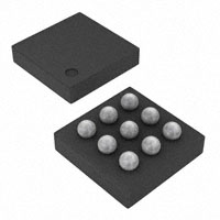
9-Ball 1,21 mm × 1,16 mm 0,4mm Pitch WCSP
Wireless or Cellular Handsets and PDAs
Portable Navigation Devices
General Portable Audio Devices
DESCRIPTION
The TPA2037D1 is a 3.2 W high efficiency filter-free
class-D audio power amplifier (class-D amp) with
6 dB of fixed gain in a 1.21 mm x 1.16 mm wafer chip
scale package (WCSP). The device requires only one
external component.
Features like 95% efficiency, 1.5 mA quiescent
current, 0.1 mA shutdown current, 81-dB PSRR,
20 mV output noise, and improved RF immunity make
the TPA2037D1 class-D amplifier ideal for cellular
handsets. A start-up time of 4 ms with no audible pop
makes the TPA2037D1 ideal for PDA and
smart-phone applications.
APPLICATION CIRCUIT
VDD
IN+
VO+
–
PWM
To battery
Cs
Internal
Oscillator
H-Bridge
VO+
TPA2037D1
9-BALL 0.4mm PITCH
WAFER CHIP SCALE PACKAGE (YFF)
(TOP VIEW OF PCB)
IN+
GND
VO-
A1
A2
A3
VDD
PVDD
PGND
B1
B2
B3
IN-
EN
VO+
C1
C2
C3
EN
Bias
Circuitry
GND
1.160 mm
IN-
TPA 2037 D1
1.214 mm
1
Please be aware that an important notice concerning availability, standard warranty, and use in critical applications of Texas
Instruments semiconductor products and disclaimers thereto appears at the end of this data sheet.
PRODUCTION DATA information is current as of publication date.
Products conform to specifications per the terms of the Texas
Instruments standard warranty. Production processing does not
necessarily include testing of all parameters.
Copyright © 2009–2010, Texas Instruments Incorporated
�TPA2037D1
SLOS648B – OCTOBER 2009 – REVISED JUNE 2010
www.ti.com
These devices have limited built-in ESD protection. The leads should be shorted together or the device placed in conductive foam
during storage or handling to prevent electrostatic damage to the MOS gates.
ORDERING INFORMATION
PACKAGED DEVICES (1)
TA
—40°C to 85°C
(1)
(2)
PART NUMBER (2)
SYMBOL
TPA2037D1YFFR
OCA
TPA2037D1YFFT
OCA
9-ball WSCP
For the most current package and ordering information, see the Package Option Addendum at the end of this document, or see the TI
Web site at www.ti.com
The YFF package is only available taped and reeled. The suffix "R" indicates a reel of 3000, the suffix "T" indicates a reel of 250.
ABSOLUTE MAXIMUM RATINGS
over operating free-air temperature range, TA = 25°C (unless otherwise noted) (1)
VALUE
UNIT
In active mode
–0.3 to 6.0
V
In shutdown mode
–0.3 to 6.0
V
VDD, PVDD
Supply voltage
VI
Input voltage
RL
Minimum load resistance
EN, IN+, IN–
Output continuous total power dissipation
–0.3 to VDD + 0.3
V
3.2
Ω
See Dissipation Rating Table
TA
Operating free-air temperature range
–40 to 85
°C
TJ
Operating junction temperature range
–40 to 150
°C
Tstg
Storage temperature range
–65 to 85
°C
(1)
Stresses beyond those listed under absolute maximum ratings may cause permanent damage to the device. These are stress ratings
only, and functional operation of the device at these or any other conditions beyond those indicated under recommended operating
conditions is not implied. Exposure to Absolute Maximum Ratings conditions for extended periods may affect device reliability.
DISSIPATION RATINGS
(1)
PACKAGE
DERATING FACTOR (1)
TA < 25°C
TA = 70°C
TA = 85°C
YFF (WCSP)
4.2 mW/°C
525 mW
336 mW
273 mW
Derating factor measure with high K board.
RECOMMENDED OPERATING CONDITIONS
VDD,
PVDD
Class-D supply voltage
VIH
High-level input voltage
EN
VIL
Low-level input voltage
EN
VIC
Common mode input voltage range
VDD = 2.5V, 5.5V, CMRR ≥ 49 dB
TA
2
MIN
MAX
2.5
5.5
1.3
UNIT
V
V
0.35
V
0.75
VDD-1.1
V
Operating free-air temperature
–40
85
°C
Submit Documentation Feedback
Copyright © 2009–2010, Texas Instruments Incorporated
Product Folder Link(s) : TPA2037D1
�TPA2037D1
www.ti.com
SLOS648B – OCTOBER 2009 – REVISED JUNE 2010
ELECTRICAL CHARACTERISTICS
TA = 25°C (unless otherwise noted)
PARAMETER
TEST CONDITIONS
|VOS|
Output offset voltage (measured
differentially)
VI = 0 V, VDD = 2.5 V to 5.5 V
|IIH|
High-level EN input current
VDD = 5.5 V, VEN = 5.5 V
|IIL|
Low-level EN input current
VDD = 5.5 V, VEN = 0 V
MIN
TYP
MAX
1
5
mV
50
mA
1
mA
VDD = 5.5 V, no load
1.8
2.5
VDD = 3.6 V, no load
1.5
2.3
I(Q)
Quiescent current
VDD = 2.5 V, no load
1.3
2.1
I(SD)
Shutdown current
VEN = 0.35 V, VDD = 3.6 V
0.1
2
RO,
Output impedance in shutdown mode
VEN = 0.35 V
f(SW)
Switching frequency
VDD = 2.5 V to 5.5 V
250
AV
Gain
VDD = 2.5 V to 5.5 V, RL = no load
5.5
REN
Resistance from EN to GND
RIN
Single ended input resistance
SD
UNIT
mA
mA
2
kΩ
300
350
6.0
6.5
kHz
dB
300
VEN ≥ VIH
150
VEN ≤ VIL
75
kΩ
kΩ
OPERATING CHARACTERISTICS
VDD = 3.6 V, TA = 25°C, RL = 8 Ω (unless otherwise noted)
PARAMETER
TEST CONDITIONS
THD + N = 10%, f = 1 kHz, RL = 4 Ω
THD + N = 1%, f = 1 kHz, RL = 4 Ω
PO
Output power
THD + N = 10%, f = 1 kHz, RL = 8 Ω
THD + N = 1%, f = 1 kHz, RL = 8 Ω
Vn
THD+N
Noise output voltage
Total harmonic distortion plus
noise
VDD = 3.6 V, Inputs AC grounded
with CI = 2mF, f = 20 Hz to 20 kHz
MIN
TYP
VDD = 5 V
3.24
VDD = 3.6 V
1.62
VDD = 2.5 V
0.70
VDD = 5 V
2.57
VDD = 3.6 V
1.32
VDD = 2.5 V
0.57
VDD = 5 V
1.80
VDD = 3.6 V
0.91
VDD = 2.5 V
0.42
VDD = 5 V
1.46
VDD = 3.6 V
0.74
VDD = 2.5 V
0.33
A-weighting
20
No weighting
26
VDD = 5.0 V, PO = 1.0 W, f = 1 kHz, RL = 8 Ω
0.12%
VDD = 3.6 V, PO = 0.5 W, f = 1 kHz, RL = 8 Ω
0.05%
VDD = 2.5 V, PO = 0.2 W, f = 1 kHz, RL = 8 Ω
0.05%
VDD = 5.0 V, PO = 2.0 W, f = 1 kHz, RL = 4 Ω
0.32%
VDD = 3.6 V, PO = 1.0 W, f = 1 kHz, RL = 4 Ω
0.11%
VDD = 2.5 V, PO = 0.4 W, f = 1 kHz, RL = 4 Ω
0.12%
MAX
UNIT
W
W
W
W
mVRMS
PSRR
AC power supply rejection ratio
VDD = 3.6 V, Inputs AC grounded with CI = 2 mF,
200 mVpp ripple, f = 217 Hz
81
dB
CMRR
Common mode rejection ratio
VDD = 3.6 V, VIC = 1 VPP, f = 217 Hz
79
dB
TSU
Startup time from shutdown
VDD = 3.6 V
4
ms
Submit Documentation Feedback
Copyright © 2009–2010, Texas Instruments Incorporated
Product Folder Link(s) : TPA2037D1
3
�TPA2037D1
SLOS648B – OCTOBER 2009 – REVISED JUNE 2010
www.ti.com
OPERATING CHARACTERISTICS (continued)
VDD = 3.6 V, TA = 25°C, RL = 8 Ω (unless otherwise noted)
PARAMETER
TEST CONDITIONS
Short circuit protection
threshold
ISC
Time for which output is
disabled after a short circuit
event, after which
auto-recovery trials are
continuously made
TAR
MIN
TYP
VDD = 3.6 V, VO+ shorted to VDD
2
VDD = 3.6 V, VO– shorted to VDD
2
VDD = 3.6 V, VO+ shorted to GND
2
VDD = 3.6 V, VO– shorted to GND
2
VDD = 3.6 V, VO+ shorted to VO–
2
VDD = 2.5 V to 5.5 V
100
MAX
UNIT
A
ms
Terminal Functions
TERMINAL
NAME
WCSP BALL
I/O
DESCRIPTION
IN–
C1
I
Negative differential audio input.
IN+
A1
I
Positive differential audio input.
VO-
A3
O
Negative BTL audio output.
VO+
C3
O
Positive BTL audio output.
GND
A2
I
Analog ground terminal. Must be connected to same potential as PGND using a direct connection
to a single point ground.
PGND
B3
I
High-current Analog ground terminal. Must be connected to same potential as GND using a direct
connection to a single point ground.
VDD
B1
I
Power supply terminal. Must be connected to same power supply as PVDD using a direct
connection. Voltage must be within values listed in Recommended Operating Conditions table.
PVDD
B2
I
High-current Power supply terminal. Must be connected to same power supply as VDD using a
direct connection. Voltage must be within values listed in Recommended Operating Conditions
table.
EN
C2
I
Enable terminal. Connect to Logic High voltage to enable device, Logic Low voltage to disable
(shutdown).
FUNCTIONAL BLOCK DIAGRAM
EN
Input
Buffer
SC
300 KΩ
4
Submit Documentation Feedback
Copyright © 2009–2010, Texas Instruments Incorporated
Product Folder Link(s) : TPA2037D1
�TPA2037D1
www.ti.com
SLOS648B – OCTOBER 2009 – REVISED JUNE 2010
TEST SETUP FOR GRAPHS
CI
+
Measurement
Output
OUT+
IN+
TPA2037D1
CI
-
IN-
+
Load
30 kHz
Low Pass
Filter
OUTVDD
Measurement
Input
-
GND
CS1
CS2
+
VDD
-
1. CI was shorted for any common-mode input voltage measurement. All other measurements were taken with CI = 0.1-mF
(unless otherwise noted).
2. CS1 = 0.1mF is placed very close to the device. The optional CS2 = 10mF is used for datasheet graphs.
3. The 30-kHz low-pass filter is required even if the analyzer has an internal low-pass filter. An RC low-pass filter (1kΩ,
4700pF) is used on each output for the data sheet graphs.
Submit Documentation Feedback
Copyright © 2009–2010, Texas Instruments Incorporated
Product Folder Link(s) : TPA2037D1
5
�TPA2037D1
SLOS648B – OCTOBER 2009 – REVISED JUNE 2010
www.ti.com
TYPICAL CHARACTERISTICS
VDD = 3.6 V, CI = 0.1 mF, CS1 = 0.1 mF, CS2 = 10 mF, TA = 25°C, RL = 8 Ω (unless otherwise noted)
EFFICIENCY
vs OUTPUT POWER
100
100
90
90
80
80
70
70
60
50
40
RL = 8 Ω + 33 µH
30
20
0.2
0.4
0.6
0.8
1.0
1.2
1.4
1.6
1.8
60
50
40
RL = 4 Ω + 33 µH
30
20
VDD = 2.5 V
VDD = 3.6 V
VDD = 5.0 V
10
0
0.0
η − Efficiency − %
η − Efficiency − %
EFFICIENCY
vs OUTPUT POWER
VDD = 2.5 V
VDD = 3.6 V
VDD = 5.0 V
10
0
0.0
2.0
0.4
0.8
1.2
PO − Output Power − W
POWER DISSIPATION
vs OUTPUT POWER
0.5
0.2
0.1
0.6
RL = 8 Ω + 33 µH
RL = 4 Ω + 33 µH
VDD = 3.6 V
0.3
0.4
0.8
1.0
1.2
1.4
3.6
4.0
1.6
1.8
0.3
0.2
0.1
0.0
0.0
2.0
VDD = 5.0 V
0.4
0.8
1.2
1.6
2.0
2.4
2.8
3.2
3.6
4.0
PO − Output Power − W
Figure 3.
Figure 4.
SUPPLY CURRENT
vs OUTPUT POWER
SUPPLY CURRENT
vs OUTPUT POWER
900m
500m
RL = 4 Ω + 33 µH
VDD = 2.5 V
VDD = 3.6 V
VDD = 5.0 V
600m
500m
400m
300m
200m
RL = 8 Ω + 33 µH
VDD = 2.5 V
VDD = 3.6 V
VDD = 5.0 V
400m
700m
IDD − Supply Current − A
IDD − Supply Current − A
3.2
0.4
PO − Output Power − W
800m
2.8
POWER DISSIPATION
vs OUTPUT POWER
RL = 8 Ω + 33 µH
RL = 4 Ω + 33 µH
0.2
2.4
Figure 2.
0.4
0.0
0.0
2.0
Figure 1.
PD − Power Dissipation − W
PD − Power Dissipation − W
0.5
1.6
PO − Output Power − W
300m
200m
100m
100m
0
0.0
0.4
0.8
1.2
1.6
2.0
2.4
2.8
3.2
3.6
4.0
0
0.0
0.2
PO − Output Power − W
0.6
0.8
1.0
1.2
1.4
1.6
1.8
2.0
PO − Output Power − W
Figure 5.
6
0.4
Figure 6.
Submit Documentation Feedback
Copyright © 2009–2010, Texas Instruments Incorporated
Product Folder Link(s) : TPA2037D1
�TPA2037D1
www.ti.com
SLOS648B – OCTOBER 2009 – REVISED JUNE 2010
TYPICAL CHARACTERISTICS (continued)
VDD = 3.6 V, CI = 0.1 mF, CS1 = 0.1 mF, CS2 = 10 mF, TA = 25°C, RL = 8 Ω (unless otherwise noted)
SUPPLY CURRENT
vs SUPPLY VOLTAGE
SUPPLY CURRENT
vs EN VOLTAGE
2.00
200
VDD = 2.5 V
VDD = 3.6 V
VDD = 5.0 V
1.75
IDD − Supply Current − nA
IDD − Supply Current − mA
RL = No Load
RL = 8 Ω + 33 µH
RL = 4 Ω + 33 µH
1.50
1.25
1.00
2.5
3.0
3.5
4.0
4.5
5.0
150
100
50
0
0.0
5.5
0.1
0.2
VDD − Supply Voltage − V
Figure 8.
OUTPUT POWER
vs LOAD RESISTANCE
OUTPUT POWER
vs LOAD RESISTANCE
0.5
4
VDD = 2.5 V
VDD = 3.6 V
VDD = 5.0 V
THD+N = 10 %
Frequency = 1 kHz
3
2
1
VDD = 2.5 V
VDD = 3.6 V
VDD = 5.0 V
THD+N = 1 %
Frequency = 1 kHz
PO − Output Power − W
PO − Output Power − W
0.4
Figure 7.
4
0
3
2
1
0
4
8
12
16
20
24
28
32
4
8
12
RL − Load Resistance − Ω
3
24
Figure 10.
OUTPUT POWER
vs SUPPLY VOLTAGE
THD + NOISE
vs OUTPUT POWER
RL = 4 Ω, THD+N = 1 %
RL = 4 Ω, THD+N = 10 %
RL = 8 Ω, THD+N = 1 %
RL = 8 Ω, THD+N = 10 %
1
Frequency = 1 kHz
3.0
20
Figure 9.
2
0
2.5
16
3.5
28
32
RL − Load Resistance − Ω
4.0
4.5
5.0
THD+N − Total Harmonic Distortion + Noise − %
4
PO − Output Power − W
0.3
VEN − EN Voltage − V
100
RL = 4 Ω + 33 µH
VDD = 2.5 V
VDD = 3.6 V
VDD = 5.0 V
10
1
0.1
0.01
10m
VDD − Supply Voltage − V
100m
1
5
PO − Output Power − W
Figure 11.
Figure 12.
Submit Documentation Feedback
Copyright © 2009–2010, Texas Instruments Incorporated
Product Folder Link(s) : TPA2037D1
7
�TPA2037D1
SLOS648B – OCTOBER 2009 – REVISED JUNE 2010
www.ti.com
TYPICAL CHARACTERISTICS (continued)
VDD = 3.6 V, CI = 0.1 mF, CS1 = 0.1 mF, CS2 = 10 mF, TA = 25°C, RL = 8 Ω (unless otherwise noted)
100
THD + NOISE
vs FREQUENCY
THD+N − Total Harmonic Distortion + Noise − %
THD+N − Total Harmonic Distortion + Noise − %
THD + NOISE
vs OUTPUT POWER
RL = 8 Ω + 33 µH
VDD = 2.5 V
VDD = 3.6 V
VDD = 5.0 V
10
1
0.1
0.01
10m
100m
1
10
1
0.1
0.01
0.001
5
20
100
THD+N − Total Harmonic Distortion + Noise − %
THD + NOISE
vs FREQUENCY
THD + NOISE
vs FREQUENCY
PO = 25 mW
PO = 125 mW
PO = 500 mW
VDD = 3.6 V
RL = 8 Ω + 33 µH
1
0.1
0.01
0.001
1k
f − Frequency − Hz
10k
0.1
0.01
0.001
20
100
THD + NOISE
vs FREQUENCY
0.1
0.01
0.001
1k
f − Frequency − Hz
10k
20k
10k
20k
10
PO = 50 mW
PO = 250 mW
PO = 1 W
VDD = 3.6 V
RL = 4 Ω + 33 µH
1
0.1
0.01
0.001
20
Figure 17.
8
1k
f − Frequency − Hz
THD + NOISE
vs FREQUENCY
1
100
1
Figure 16.
PO = 100 mW
PO = 500 mW
PO = 2 W
20k
PO = 15 mW
PO = 75 mW
PO = 200 mW
VDD = 2.5 V
RL = 8 Ω + 33 µH
Figure 15.
VDD = 5.0 V
RL = 4 Ω + 33 µH
10k
10
20k
10
20
THD+N − Total Harmonic Distortion + Noise − %
Figure 14.
10
100
1k
f − Frequency − Hz
Figure 13.
THD+N − Total Harmonic Distortion + Noise − %
THD+N − Total Harmonic Distortion + Noise − %
PO − Output Power − W
20
PO = 50 mW
PO = 250 mW
PO = 1 W
VDD = 5.0 V
RL = 8 Ω + 33 µH
100
1k
f − Frequency − Hz
10k
20k
Figure 18.
Submit Documentation Feedback
Copyright © 2009–2010, Texas Instruments Incorporated
Product Folder Link(s) : TPA2037D1
�TPA2037D1
www.ti.com
SLOS648B – OCTOBER 2009 – REVISED JUNE 2010
TYPICAL CHARACTERISTICS (continued)
VDD = 3.6 V, CI = 0.1 mF, CS1 = 0.1 mF, CS2 = 10 mF, TA = 25°C, RL = 8 Ω (unless otherwise noted)
THD + NOISE vs
COMMON MODE INPUT VOLTAGE
10
PO = 30 mW
PO = 150 mW
PO = 400 mW
VDD = 2.5 V
RL = 4 Ω + 33 µH
1
0.1
0.01
0.001
20
100
1k
f − Frequency − Hz
10k
THD+N − Total Harmonic Distortion + Noise − %
THD+N − Total Harmonic Distortion + Noise − %
THD + NOISE
vs FREQUENCY
20k
VDD = 2.5 V
VDD = 3.6 V
VDD = 5.0 V
1
0.1
0.01
0.0
0.5
1.0
1.5
2.0
2.5
3.0
3.5
4.0
4.5
Figure 19.
Figure 20.
POWER SUPPLY REJECTION RATIO
vs FREQUENCY
POWER SUPPLY REJECTION RATIO
vs FREQUENCY
5.0
0
Inputs AC−Grounded
CI = 2 µF
RL = 8 Ω + 33 µH
−10
−20
VDD = 2.5 V
VDD = 3.6 V
VDD = 5.0 V
−30
−40
−50
−60
−70
−80
−90
PSRR − Power Supply Rejection Ratio − dB
PSRR − Power Supply Rejection Ratio − dB
RL = 8 Ω + 33 µH
Frequency = 1 kHz
PO = 200 mW
VIC − Common Mode Input Voltage − V
0
−100
Inputs AC−Grounded
CI = 2 µF
RL = 4 Ω + 33 µH
−10
−20
VDD = 2.5 V
VDD = 3.6 V
VDD = 5.0 V
−30
−40
−50
−60
−70
−80
−90
−100
20
−10
100
1k
f − Frequency − Hz
10k
20k
100
1k
f − Frequency − Hz
10k
Figure 21.
Figure 22.
POWER SUPPLY REJECTION RATIO
vs COMMON MODE INPUT VOLTAGE
COMMON MODE REJECTION RATIO
vs FREQUENCY
RL = 8 Ω + 33 µH
Frequency = 217 Hz
VDD = 2.5 V
VDD = 3.6 V
VDD = 5.0 V
−20
−30
−40
−50
−60
−70
−80
−90
−100
0.0
20
CMRR − Common Mode Rejection Ratio − dB
0
PSRR − Power Supply Rejection Ratio − dB
10
20k
−30
VIC = 1 VPP
RL = 8 Ω + 33 µH
−40
VDD = 2.5 V
VDD = 3.6 V
VDD = 5.0 V
−50
−60
−70
−80
−90
−100
0.5
1.0
1.5
2.0
2.5
3.0
3.5
4.0
4.5
5.0
20
VIC − Common Mode Input Voltage − V
Figure 23.
100
1k
f − Frequency − Hz
10k
20k
Figure 24.
Submit Documentation Feedback
Copyright © 2009–2010, Texas Instruments Incorporated
Product Folder Link(s) : TPA2037D1
9
�TPA2037D1
SLOS648B – OCTOBER 2009 – REVISED JUNE 2010
www.ti.com
TYPICAL CHARACTERISTICS (continued)
VDD = 3.6 V, CI = 0.1 mF, CS1 = 0.1 mF, CS2 = 10 mF, TA = 25°C, RL = 8 Ω (unless otherwise noted)
COMMON MODE REJECTION RATIO
vs COMMON MODE INPUT VOLTAGE
CMRR − Common Mode Rejection Ratio − dB
0
RL = 8 Ω + 33 µH
Frequency = 217 Hz
−10
VDD = 2.5 V
VDD = 3.6 V
VDD = 5.0 V
−20
−30
−40
−50
−60
−70
−80
−90
−100
0.0
0.5
1.0
1.5
2.0
2.5
3.0
3.5
4.0
4.5
5.0
VIC − Common Mode Input Voltage − V
Figure 25.
GSM POWER SUPPLY REJECTION
vs TIME
C1 - High
3.6 V
VDD
500 mV/div
C1 - Amplitude
500 mV
C1 - Duty Cycle
20%
VOUT
500 mV/div
0
2.5
5
7.5
10
12.5
15
17.5
20
22.5
25
t − Time − ms
G026
Figure 26.
0
−25
−50
−75
−100
VO − Output Voltage − dBV
−125
−25
−150
−50
−175
VDD − Supply Voltage − dBV
GSM POWER SUPPLY REJECTION
vs FREQUENCY
−75
−100
−125
−150
−175
−200
0
2.4
4.8
7.2
9.6
12
14.4
16.8
19.2
21.6
24
f − Frequency − kHz
G027
Figure 27.
10
Submit Documentation Feedback
Copyright © 2009–2010, Texas Instruments Incorporated
Product Folder Link(s) : TPA2037D1
�TPA2037D1
www.ti.com
SLOS648B – OCTOBER 2009 – REVISED JUNE 2010
APPLICATION INFORMATION
SHORT CIRCUIT AUTO-RECOVERY
When a short-circuit event occurs, the TPA2037D1 goes to shutdown mode and activates the integrated
auto-recovery process whose aim is to return the device to normal operation once the short-circuit is removed.
This process repeatedly examines (once every 100ms) whether the short-circuit condition persists, and returns
the device to normal operation immediately after the short-circuit condition is removed. This feature helps protect
the device from large currents and maintain a good long-term reliability.
INTEGRATED IMAGE REJECT FILTER FOR DAC NOISE REJECTION
In applications which use a DAC to drive Class-D amplifiers, out-of-band noise energy present at the DAC's
image frequencies fold back into the audio-band at the output of the Class-D amplifier. An external low-pass filter
is often placed between the DAC and the Class-D amplifier in order to attenuate this noise.
The TPA2037D1 has an integrated Image Reject Filter with a low-pass cutoff frequency of 130 kHz, which
significantly attenuates this noise. Depending on the system noise specification, the integrated Image Reject
Filter may help eliminate external filtering, thereby saving board space and component cost.
COMPONENT SELECTION
Figure 28 shows the TPA2037D1 typical schematic with differential inputs, while Figure 29 shows the
TPA2037D1 with differential inputs and input capacitors. Figure 30 shows the TPA2037D1 with a single-ended
input.
Decoupling Capacitors (CS1, CS2)
The TPA2037D1 is a high-performance class-D audio amplifier that requires adequate power supply decoupling
to ensure the efficiency is high and total harmonic distortion (THD) is low. For higher frequency transients,
spikes, or digital hash on the line, a good low equivalent-series-resistance (ESR) ceramic capacitor CS1 = 0.1mF ,
placed as close as possible to the device VDD lead works best. Placing CS1 close to the TPA2037D1 is important
for the efficiency of the class-D amplifier, because any resistance or inductance in the trace between the device
and the capacitor can cause a loss in efficiency. For filtering lower-frequency noise signals, a 10 mF or greater
capacitor (CS2) placed near the audio power amplifier would also help, but it is not required in most applications
because of the high PSRR of this device. Typically, the smaller the capacitor's case size, the lower the
inductance and the closer it can be placed to the TPA2037D1. X5R and X7R dielectric capacitors are
recommended for both CS1 and CS2.
Input Capacitors (CI)
The TPA2037D1 does not require input coupling capacitors if the design uses a differential source that is biased
within the common-mode input voltage range. That voltage range is listed in the Recommended Operating
Conditions table. If the input signal is not biased within the recommended common-mode input range, such as in
needing to use the input as a high pass filter, shown in Figure 29, or if using a single-ended source, shown in
Figure 30, input coupling capacitors are required. The same value capacitors should be used on both IN+ and
IN– for best pop performance. The 3-dB high-pass cutoff frequency fC of the filter formed by the input coupling
capacitor CI and the input resistance RI (typically 150 kΩ) of the TPA2037D1 is given by Equation 1:
1
fC =
(2πRICI )
(1)
The value of the input capacitor is important to consider as it directly affects the bass (low frequency)
performance of the circuit. Speaker response may also be taken into consideration when setting the corner
frequency using input capacitors. Solving for the input coupling capacitance, we get:
1
CI =
2πR
( IfC )
(2)
If the corner frequency is within the audio band, the capacitors should have a tolerance of ±10% or better,
because any mismatch in capacitance causes an impedance mismatch at the corner frequency and below.
Submit Documentation Feedback
Copyright © 2009–2010, Texas Instruments Incorporated
Product Folder Link(s) : TPA2037D1
11
�TPA2037D1
SLOS648B – OCTOBER 2009 – REVISED JUNE 2010
www.ti.com
For a flat low-frequency response, use large input coupling capacitors (0.1 mF or larger). X5R and X7R dielectric
capacitors are recommended.
To Battery
Internal
Oscillator
VDD
CS
IN−
PWM
_
Differential
Input
H−
Bridge
VO−
VO+
+
IN+
GND
Bias
Circuitry
EN
TPA2037D1
Filter-Free Class D
Figure 28. Typical TPA2037D1 Application Schematic With DC-coupled Differential Input
To Battery
CI
Internal
Oscillator
CS
IN−
PWM
_
Differential
Input
VDD
CI
H−
Bridge
VO−
VO+
+
IN+
GND
EN
Bias
Circuitry
TPA2037D1
Filter-Free Class D
Figure 29. TPA2037D1 Application Schematic With Differential Input and Input Capacitors
CI
Single-ended
Input
To Battery
Internal
Oscillator
VDD
IN−
_
PWM
H−
Bridge
CS
VO−
VO+
+
IN+
CI
GND
EN
Bias
Circuitry
TPA2037D1
Filter-Free Class D
Figure 30. TPA2037D1 Application Schematic With Single-Ended Input
12
Submit Documentation Feedback
Copyright © 2009–2010, Texas Instruments Incorporated
Product Folder Link(s) : TPA2037D1
�TPA2037D1
www.ti.com
SLOS648B – OCTOBER 2009 – REVISED JUNE 2010
EFFICIENCY AND THERMAL INFORMATION
The maximum ambient operating temperature of the TPA2037D1 depends on the load resistance, power supply
voltage and heat-sinking ability of the PCB system. The derating factor for the YFF package is shown in the
dissipation rating table. Converting this to qJA:
1
q
+
JA
Derating Factor
(3)
Given qJA (from the Package Dissipation ratings table), the maximum allowable junction temperature (from the
Absolute Maximum ratings table), and the maximum internal dissipation (from Power Dissipation vs Output
Power figures) the maximum ambient temperature can be calculated with the following equation. Note that the
units on these figures are Watts RMS. Because of crest factor (ratio of peak power to RMS power) from 9–15
dB, thermal limitations are not usually encountered.
T Max + T Max * q P
A
J
JA Dmax
(4)
The TPA2037D1 is designed with thermal protection that turns the device off when the junction temperature
surpasses 150°C to prevent damage to the IC. Note that the use of speakers less resistive than 4-Ω (typ) is not
advisable. Below 4-Ω (typ) the thermal performance of the device dramatically reduces because of increased
output current and reduced amplifier efficiency. The Absolute Maximum rating of 3.2-Ω covers the manufacturing
tolerance of a 4-Ω speaker and speaker impedance decrease due to frequency. qJA is a gross approximation of
the complex thermal transfer mechanisms between the device and its ambient environment. If the qJA calculation
reveals a potential problem, a more accurate estimate should be made.
WHEN TO USE AN OUTPUT FILTER
Design the TPA2037D1 without an Inductor / Capacitor (LC) output filter if the traces from the amplifier to the
speaker are short. Wireless handsets and PDAs are great applications for this class-D amplifier to be used
without an output filter.
The TPA2037D1 does not require an LC output filter for short speaker connections (approximately 100 mm long
or less). A ferrite bead can often be used in the design if failing radiated emissions testing without an LC filter;
and, the frequency-sensitive circuit is greater than 1 MHz. If choosing a ferrite bead, choose one with high
impedance at high frequencies, but very low impedance at low frequencies. The selection must also take into
account the currents flowing through the ferrite bead. Ferrites can begin to loose effectiveness at much lower
than rated current values. See the EVM User's Guide (SLOU266) for components used successfully by TI.
Figure 31 shows a typical ferrite-bead output filter.
Ferrite
Chip Bead
VO−
1 nF
Ferrite
Chip Bead
VO+
1 nF
Figure 31. Typical Ferrite Chip Bead Filter
Submit Documentation Feedback
Copyright © 2009–2010, Texas Instruments Incorporated
Product Folder Link(s) : TPA2037D1
13
�TPA2037D1
SLOS648B – OCTOBER 2009 – REVISED JUNE 2010
www.ti.com
PRINTED CIRCUIT BOARD LAYOUT
In making the pad size for the WCSP balls, it is recommended that the layout use nonsolder mask defined
(NSMD) land. With this method, the solder mask opening is made larger than the desired land area, and the
opening size is defined by the copper pad width. Figure 32 shows the appropriate diameters for a WCSP layout.
Figure 32. Land Pattern Image and Dimensions
SOLDER PAD
DEFINITIONS
COPPER PAD
SOLDER MASK
OPENING(5)
COPPER
THICKNESS
STENCIL OPENING(6) (7)
STENCIL
THICKNESS
Nonsolder mask
defined (NSMD)
0.23 mm
0.310 mm
1 oz max
(0.032 mm)
0.275 mm x 0.275 mm Sq.
(rounded corners)
0.1 mm thick
1. Circuit traces from NSMD defined PWB lands should be 75 mm to 100 mm wide in the exposed area inside
the solder mask opening. Wider trace widths reduce device stand off and impact reliability.
2. Best reliability results are achieved when the PWB laminate glass transition temperature is above the
operating the range of the intended application.
3. Recommend solder paste is Type 3 or Type 4.
4. For a PWB using a Ni/Au surface finish, the gold thickness should be less 0.5 mm to avoid a reduction in
thermal fatigue performance.
5. Solder mask thickness should be less than 20 mm on top of the copper circuit pattern
6. Best solder stencil performance is achieved using laser cut stencils with electro polishing. Use of chemically
etched stencils give inferior solder paste volume control.
7. Trace routing away from WCSP device should be balanced in X and Y directions to avoid unintentional
component movement due to solder wetting forces.
Figure 33. Layout Snapshot
An on-pad via is not required to route the middle ball B2 (PVDD) of the TPA2037D1. Just short ball B2 (PVDD) to
ball B1 (VDD) and connect both to the supply trace as shown in Figure 33. This simplifies board routing and
saves manufacturing cost.
14
Submit Documentation Feedback
Copyright © 2009–2010, Texas Instruments Incorporated
Product Folder Link(s) : TPA2037D1
�TPA2037D1
www.ti.com
SLOS648B – OCTOBER 2009 – REVISED JUNE 2010
PACKAGE DIMENSIONS
D
E
Max = 1190µm
Max = 1244µm
Min = 1130µm
Min = 1184µm
REVISION HISTORY
Changes from Original (October 2009) to Revision A
Page
•
Changed graph using supplied data ................................................................................................................................... 10
•
Changed graph using supplied data ................................................................................................................................... 10
•
Added package dimensions table ....................................................................................................................................... 15
Changes from Revision A (December 2009) to Revision B
•
Page
Changed the Package Dimensions table. D was Max = 1244mm, Min = 1184mm. E was Max = 1190mm, Min =
1130mm ............................................................................................................................................................................... 15
Submit Documentation Feedback
Copyright © 2009–2010, Texas Instruments Incorporated
Product Folder Link(s) : TPA2037D1
15
�PACKAGE OPTION ADDENDUM
www.ti.com
10-Dec-2020
PACKAGING INFORMATION
Orderable Device
Status
(1)
Package Type Package Pins Package
Drawing
Qty
Eco Plan
(2)
Lead finish/
Ball material
MSL Peak Temp
Op Temp (°C)
Device Marking
(3)
(4/5)
(6)
TPA2037D1YFFR
ACTIVE
DSBGA
YFF
9
3000
RoHS & Green
SNAGCU
Level-1-260C-UNLIM
-40 to 85
OCA
TPA2037D1YFFT
ACTIVE
DSBGA
YFF
9
250
RoHS & Green
SNAGCU
Level-1-260C-UNLIM
-40 to 85
OCA
(1)
The marketing status values are defined as follows:
ACTIVE: Product device recommended for new designs.
LIFEBUY: TI has announced that the device will be discontinued, and a lifetime-buy period is in effect.
NRND: Not recommended for new designs. Device is in production to support existing customers, but TI does not recommend using this part in a new design.
PREVIEW: Device has been announced but is not in production. Samples may or may not be available.
OBSOLETE: TI has discontinued the production of the device.
(2)
RoHS: TI defines "RoHS" to mean semiconductor products that are compliant with the current EU RoHS requirements for all 10 RoHS substances, including the requirement that RoHS substance
do not exceed 0.1% by weight in homogeneous materials. Where designed to be soldered at high temperatures, "RoHS" products are suitable for use in specified lead-free processes. TI may
reference these types of products as "Pb-Free".
RoHS Exempt: TI defines "RoHS Exempt" to mean products that contain lead but are compliant with EU RoHS pursuant to a specific EU RoHS exemption.
Green: TI defines "Green" to mean the content of Chlorine (Cl) and Bromine (Br) based flame retardants meet JS709B low halogen requirements of


 工商网监
湘ICP备2023018690号
工商网监
湘ICP备2023018690号
