TPA4411
TPA4411M
www.ti.com
SLOS430E – AUGUST 2004 – REVISED MARCH 2008
80-mW DIRECTPATH™ STEREO HEADPHONE DRIVER
FEATURES
16
18
17
20
19
17
16
18
20
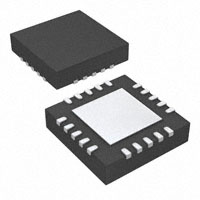
• Space Saving Packages
– 20-Pin, 4 mm × 4 mm Thin QFN
– TPA4411 – Thermally Optimized
PowerPAD™ Package
– TPA4411M – Thermally Enhanced
PowerPAD™ Package
– 16-Ball, 2.18 mm × 2.18 mm WCSP
• Ground-Referenced Outputs Eliminate
DC-Bias Voltages on Headphone Ground Pin
– No Output DC-Blocking Capacitors
– Reduced Board Area
– Reduced Component Cost
– Improved THD+N Performance
– No Degradation of Low-Frequency
Response Due to Output Capacitors
• Wide Power Supply Range: 1.8 V to 4.5 V
• 80-mW/Ch Output Power into 16-Ω at 4.5 V
• Independent Right and Left Channel
Shutdown Control
• Short-Circuit and Thermal Protection
• Pop Reduction Circuitry
19
1
2
APPLICATIONS
•
•
•
•
•
Notebook Computers
CD / MP3 Players
Smart Phones
Cellular Phones
PDAs
4
12
5
11
5
11
6
TPA4411RTJ
TPA4411MRTJ
A2
A3
A4
INR
SGND
PVDD
C1P
B1
SDR
SDL
NC
PGND
C1
INL
OUTR
NC
C1N
D1
SVDD
OUTL
SVSS
PVSS
A1
10
12
8
13
4
9
3
7
13
10
14
3
9
15
2
8
1
14
6
15
2
7
1
TPA4411YZH
DESCRIPTION
The TPA4411 and TPA4411M are stereo headphone
drivers designed to allow the removal of the output
DC-blocking capacitors for reduced component count
and cost. The TPA4411 and TPA4411M are ideal for
small portable electronics where size and cost are
critical design parameters.
The TPA4411 and TPA4411M are capable of driving
80 mW into a 16-Ω load at 4.5 V. Both TPA4411 and
TPA4411M have a fixed gain of –1.5 V/V and
headphone outputs that have ±8-kV IEC ESD
protection. The TPA4411 and TPA4411M have
independent shutdown control for the right and left
audio channels.
The TPA4411 is available in a 2.18 mm × 2.18 mm
WCSP and 4 mm × 4 mm Thin QFN packages. The
TPA4411M is available in a 4 mm × 4 mm Thin QFN
package. The TPA4411RTJ package is a thermally
optimized PowerPAD™ package allowing the
maximum amount of thermal dissipation and the
TPA4411MRTJ is a thermally enhanced PowerPAD
package designed to match competitive package
footprints.
1
2
Please be aware that an important notice concerning availability, standard warranty, and use in critical applications of
Texas Instruments semiconductor products and disclaimers thereto appears at the end of this data sheet.
PowerPAD, DirectPath are trademarks of Texas Instruments.
PRODUCTION DATA information is current as of publication date.
Products conform to specifications per the terms of the Texas
Instruments standard warranty. Production processing does not
necessarily include testing of all parameters.
Copyright © 2004–2008, Texas Instruments Incorporated
�TPA4411
TPA4411M
www.ti.com
SLOS430E – AUGUST 2004 – REVISED MARCH 2008
These devices have limited built-in ESD protection. The leads should be shorted together or the device placed in conductive foam
during storage or handling to prevent electrostatic damage to the MOS gates.
PVSS
5
PVDD
SDL
SGND
NC
18
17
16
C1N
3
13
INL
12
NC
NC
4
12
NC
11
OUTR
PVSS
5
11
OUTR
TPA4411RTJ
10
INL
SVDD
SDR
9
14
OUTL
2
NC
PGND
8
INR
6
15
NC
NC
19
NC
16
4
10
NC
SVDD
13
1
7
SGND
17
3
9
C1N
OUTL
SDR
C1P
SVSS
SDL
18
14
8
2
NC
PGND
NC
PVDD
19
INR
7
15
SVSS
1
6
C1P
20
NC
20
RTJ (QFN) PACKAGE
(TOP VIEW)
TPA4411MRTJ
NC − No internal connection
NC − No internal connection
YZH (WCSP) PACKAGE
(TOP VIEW)
A2
A3
A4
A1
INR
SGND
PVDD
C1P
B1
SDR
SDL
NC
PGND
C1
INL
OUTR
NC
C1N
D1
SVDD
OUTL
SVSS
PVSS
TPA4411YZH
NC - No internal connection
2
Copyright © 2004–2008, Texas Instruments Incorporated
Product Folder Link(s): TPA4411 TPA4411M
�TPA4411
TPA4411M
www.ti.com
SLOS430E – AUGUST 2004 – REVISED MARCH 2008
TERMINAL FUNCTIONS
TERMINAL
NAME
I/O DESCRIPTION
QFN
WCSP
C1P
1
A4
PGND
2
B4
C1N
3
C4
NC
4, 6, 8,
12, 16,
20
B3, C3
PVSS
5
D4
O
Output from charge pump.
SVSS
7
D3
I
Amplifier negative supply, connect to PVSS via star connection.
OUTL
9
D2
O
Left audio channel output signal
SVDD
10
D1
I
Amplifier positive supply, connect to PVDD via star connection.
OUTR
11
C2
O
Right audio channel output signal
INL
13
C1
I
Left audio channel input signal
SDR
14
B1
I
Right channel shutdown, active low logic.
INR
15
A1
I
Right audio channel input signal
SGND
17
A2
I
Signal ground, connect to ground.
SDL
18
B2
I
Left channel shutdown, active low logic.
PVDD
19
A3
I
Supply voltage, connect to positive supply.
Exposed Pad
I/O Charge pump flying capacitor positive terminal
I
Power ground, connect to ground.
I/O Charge pump flying capacitor negative terminal
No connection
-
Exposed pad must be soldered to a floating plane. Do NOT connect to power or ground.
ABSOLUTE MAXIMUM RATINGS (1)
over operating free-air temperature range, TA = 25°C (unless otherwise noted)
VALUE / UNIT
Supply voltage, AVDD, PVDD
VI
–0.3 V to 5.5 V
Input voltage
–0.3 V to VDD + 0.3 V
Output Continuous total power dissipation
See Dissipation Rating Table
TA
Operating free-air temperature range
–40°C to 85°C
TJ
Operating junction temperature range
–40°C to 150°C
Tstg
Storage temperature range
–65°C to 150°C
Lead temperature 1,6 mm (1/16 inch) from case for 10 seconds
(1)
260°C
Stresses beyond those listed under absolute maximum ratings may cause permanent damage to the device. These are stress ratings
only, and functional operation of the device at these or any other conditions beyond those indicated under recommended operating
conditions is not implied. Exposure to absolute-maximum-rated conditions for extended periods may affect device reliability.
Copyright © 2004–2008, Texas Instruments Incorporated
Product Folder Link(s): TPA4411 TPA4411M
3
�TPA4411
TPA4411M
www.ti.com
SLOS430E – AUGUST 2004 – REVISED MARCH 2008
DISSIPATION RATINGS TABLE
PACKAGE
TA ≤ 25°C
POWER RATING
DERATING FACTOR (1)
TA = 70°C
POWER RATING
TA = 85°C
POWER RATING
RTJ
(TPA4411)
5200 mW
41.6 mW/°C
3120 mW
2700 mW
RTJ
(TPA4411M)
3450 mW
34.5 mW/°C
1898 mW
1380 mW
YZH
1200 mW
9.21 mW/°C
690 mW
600 mW
(1)
Derating factor measured with High K board.
AVAILABLE OPTIONS
PACKAGED DEVICES (1)
PART NUMBER
SYMBOL
20-pin, 4 mm × 4 mm QFN
TPA4411RTJ (2)
AKQ
20-pin, 4 mm × 4 mm QFN
TPA4411MRTJ (2)
BPB
16-ball, 2.18 mm × 2.18 mm WSCP
TPA4411YZH
AKT
TA
–40°C to 85°C
(1)
(2)
For the most current package and ordering information, see the Package Option Addendum at the end of this document, or see the TI
website at www.ti.com.
The RTJ package is only available taped and reeled. To order, add the suffix “R” to the end of the part number for a reel of 3000, or add
the suffix “T” to the end of the part number for a reel of 250 (e.g., TPA4411RTJR).
RECOMMENDED OPERATING CONDITIONS
MIN
MAX
UNIT
Supply voltage, AVDD, PVDD
1.8
4.5 (1)
V
VIH
High-level input voltage
SDL, SDR
1.5
VIL
Low-level input voltage
SDL, SDR
TA
Operating free-air temperature
(1)
V
0.5
V
–40
85
°C
TYP
MAX
Device can shut down for VDD > 4.5 V to prevent damage to the device.
ELECTRICAL CHARACTERISTICS
TA = 25°C (unless otherwise noted)
PARAMETER
TEST CONDITIONS
MIN
Output offset voltage
VDD = 1.8 V to 4.5 V, Inputs grounded
PSRR
Power Supply Rejection Ratio
VDD = 1.8 V to 4.5 V
–69
VOH
High-level output voltage
VDD = 3 V, RL = 16 Ω
2.2
VOL
Low-level output voltage
VDD = 3 V, RL = 16 Ω
–1.1
V
|IIH|
High-level input current (SDL, SDR)
VDD = 4.5 V, VI = VDD
1
µA
|IIL|
Low-level input current (SDL, SDR)
VDD = 4.5 V, VI = 0 V
1
µA
IDD
Supply Current
–80
mV
dB
V
VDD = 1.8 V, No load, SDL= SDR = VDD
5.3
6.5
VDD = 3 V, No load, SDL = SDR = VDD
6.5
8.0
VDD = 4.5 V, No load, SDL = SDR = VDD
8.0
10.0
Shutdown mode, VDD = 1.8 V to 4.5 V
4
8
UNIT
|VOS|
1
mA
µA
Copyright © 2004–2008, Texas Instruments Incorporated
Product Folder Link(s): TPA4411 TPA4411M
�TPA4411
TPA4411M
www.ti.com
SLOS430E – AUGUST 2004 – REVISED MARCH 2008
OPERATING CHARACTERISTICS
VDD = 3 V , TA = 25°C, RL = 16 Ω (unless otherwise noted)
PARAMETER
TEST CONDITIONS
MIN
THD = 1%, VDD = 3 V, f = 1 kHz
PO
100
THD = 1%, VDD = 3 V, f = 1 kHz, RL = 32
Ω
THD+N
Total harmonic distortion plus noise
Crosstallk
kSVR
Supply ripple rejection ratio
Av
Closed-loop voltage gain
ΔAv
Gain matching
PO = 25 mW, f = 1 kHz
0.054%
PO = 25 mW, f = 20 kHz
0.010%
PO = 20 mW, f = 1 kHz
–82.5
200-mVpp ripple, f = 1 kHz
–70.4
dB
dB
–45.1
–1.5
–1.55
V/V
1%
Slew rate
2.2
Maximum capacitive load
400
pF
10
µVRMS
Noise output voltage
OUTR, OUTL
Charge pump switching frequency
V/µs
±8
280
Start-up time from shutdown
320
kV
420
kHz
18
kΩ
450
Input impedance
SNR
mW
–83
200-mVpp ripple, f = 217 Hz
–1.45
Electrostatic discharge, IEC
fosc
UNIT
50
200-mVpp ripple, f = 20 kHz
Vn
MAX
50
THD = 1%, VDD = 4.5 V, f = 1 kHz
Output power (Outputs In Phase)
TYP
12
Signal-to-noise ratio
Po = 40 mW (THD+N = 0.1%)
Threshold
Thermal shutdown
Hysteresis
Copyright © 2004–2008, Texas Instruments Incorporated
Product Folder Link(s): TPA4411 TPA4411M
15
µs
98
150
dB
170
15
°C
°C
5
�TPA4411
TPA4411M
www.ti.com
SLOS430E – AUGUST 2004 – REVISED MARCH 2008
Functional Block Diagram
TPA4411
SVDD
Audio In − R
_
Audio Out − R
+
Short
Circuit
Protection
SVSS
SVDD
SGND
+
_
Audio In − L
Audio Out − L
SVSS
C1P
Av = −1.5 V/V
Charge
Pump
Bias
Circuitry
SDx
C1N
PVSS
APPLICATION CIRCUIT
TLV320AIC26
or
TLV320AIC28
HPL
or
SPK1
TPA2012D2
HPR
or
SPK2
Shutdown
Control
SDL
SDR
PGND
SGND
TPA4411
OUTL
INR
OUTR
INL
1.8 − 4.5 V
PVSS
SVSS
PVDD
SVDD
C1P
6
C1N
Copyright © 2004–2008, Texas Instruments Incorporated
Product Folder Link(s): TPA4411 TPA4411M
�TPA4411
TPA4411M
www.ti.com
SLOS430E – AUGUST 2004 – REVISED MARCH 2008
TYPICAL CHARACTERISTICS
C(PUMP) = C(PVSS) = 2.2 µF , CIN = 1 µF (unless otherwise noted)
Table of Graphs
FIGURE
Total harmonic distortion + noise
vs Output power
1–24
Total harmonic distortion + noise
vs Frequency
25–32
Supply voltage rejection ratio
vs Frequency
33, 34
Power dissipation
vs Output power
35–42
Crosstalk
vs Frequency
43–46
Output power
vs Supply voltage
47–50
Quiescent supply current
vs Supply voltage
51
Output power
vs Load resistance
5–60
Output spectrum
61
Gain and phase
vs Frequency
VDD = 1.8 V,
RL = 16 Ω,
fIN = 20 Hz
10
In Phase
1
Single
Channel
0.1
0.01
180° Out of Phase
0.001
1
10
30
100
VDD = 1.8 V,
RL = 16 Ω,
fIN = 1 kHz
180° Out of Phase
10
1
In Phase
0.1
Single Channel
0.01
1
10
30
100
VDD = 1.8 V,
RL = 16 Ω,
fIN = 10 kHz
In Phase
10
180° Out of Phase
1
0.1
Single Channel
0.01
1
10
30
PO − Output Power − mW
PO − Output Power − mW
Figure 2.
Figure 3.
TOTAL HARMONIC DISTORTION
+ NOISE
vs
OUTPUT POWER
TOTAL HARMONIC DISTORTION
+ NOISE
vs
OUTPUT POWER
TOTAL HARMONIC DISTORTION
+ NOISE
vs
OUTPUT POWER
100
VDD = 1.8 V,
RL = 32 Ω,
fIN = 20 Hz
10
In Phase
180° Out of Phase
1
Single Channel
0.1
0.01
0.001
1
10
30
100
VDD = 1.8 V,
RL = 32 Ω,
fIN = 1 kHz
In Phase
10
180° Out of Phase
Single Channel
1
0.1
0.01
1
10
30
PO − Output Power − mW
PO − Output Power − mW
Figure 4.
Figure 5.
Copyright © 2004–2008, Texas Instruments Incorporated
Product Folder Link(s): TPA4411 TPA4411M
THD+N − Total Harmonic Distortion + Noise − %
Figure 1.
THD+N − Total Harmonic Distortion + Noise − %
THD+N − Total Harmonic Distortion + Noise − %
PO − Output Power − mW
TOTAL HARMONIC DISTORTION
+ NOISE
vs
OUTPUT POWER
THD+N − Total Harmonic Distortion + Noise − %
100
TOTAL HARMONIC DISTORTION
+ NOISE
vs
OUTPUT POWER
THD+N − Total Harmonic Distortion + Noise − %
THD+N − Total Harmonic Distortion + Noise − %
TOTAL HARMONIC DISTORTION
+ NOISE
vs
OUTPUT POWER
62, 63
100
VDD = 1.8 V,
RL = 32 Ω,
fIN = 10 kHz
In Phase
10
180° Out of Phase
1
Single Channel
0.1
0.01
1
10
PO − Output Power − mW
30
Figure 6.
7
�TPA4411
TPA4411M
www.ti.com
SLOS430E – AUGUST 2004 – REVISED MARCH 2008
10
In Phase
1
0.1
180° Out of Phase
0.01
Single Channel
0.001
1
10
100
PO − Output Power − mW
100
VDD = 3 V,
RL = 16 Ω,
fIN = 1 kHz
In Phase
10
1
180° Out of Phase
0.1
Single Channel
0.01
1
10
100
PO − Output Power − mW
300
100
VDD = 3 V,
RL = 16 Ω,
fIN = 10 kHz
In Phase
10
1
180° Out of Phase
0.1
Single Channel
0.01
1
10
100
300
PO − Output Power − mW
Figure 9.
TOTAL HARMONIC DISTORTION
+ NOISE
vs
OUTPUT POWER
TOTAL HARMONIC DISTORTION
+ NOISE
vs
OUTPUT POWER
TOTAL HARMONIC DISTORTION
+ NOISE
vs
OUTPUT POWER
100
VDD = 3 V,
RL = 32 Ω,
fIN = 20 Hz
10
In Phase
180° Out of Phase
1
0.1
Single Channel
0.01
0.001
1
10
100
PO − Output Power − mW
300
100
VDD = 3 V,
RL = 32 Ω,
fIN = 1 kHz
In Phase
10
Single Channel
1
180° Out of Phase
0.1
0.01
1
10
100
300
THD+N − Total Harmonic Distortion + Noise − %
Figure 8.
THD+N − Total Harmonic Distortion + Noise − %
Figure 7.
100
VDD = 3 V,
RL = 32 Ω,
fIN = 10 kHz
10
In Phase
1
0.1
Single Channel
0.01
180° Out of Phase
0.001
1
PO − Output Power − mW
10
100
300
PO − Output Power − mW
Figure 11.
Figure 12.
TOTAL HARMONIC DISTORTION
+ NOISE
vs
OUTPUT POWER
TOTAL HARMONIC DISTORTION
+ NOISE
vs
OUTPUT POWER
TOTAL HARMONIC DISTORTION
+ NOISE
vs
OUTPUT POWER
100
VDD = 3.6 V,
RL = 16 Ω,
fIN = 20 Hz
10
In Phase
180° Out of Phase
1
Single Channel
0.1
0.01
0.001
1
10
100
Figure 13.
300
100
VDD = 3.6 V,
RL = 16 Ω,
fIN = 1 kHz
10
In Phase
180° Out of Phase
1
Single Channel
0.1
0.01
1
10
100
300
PO − Output Power − mW
THD+N − Total Harmonic Distortion + Noise − %
Figure 10.
PO − Output Power − mW
8
300
TOTAL HARMONIC DISTORTION
+ NOISE
vs
OUTPUT POWER
THD+N − Total Harmonic Distortion + Noise − %
VDD = 3 V,
RL = 16 Ω,
fIN = 20 Hz
THD+N − Total Harmonic Distortion + Noise − %
100
TOTAL HARMONIC DISTORTION
+ NOISE
vs
OUTPUT POWER
THD+N − Total Harmonic Distortion + Noise − %
THD+N − Total Harmonic Distortion + Noise − %
THD+N − Total Harmonic Distortion + Noise − %
THD+N − Total Harmonic Distortion + Noise − %
TOTAL HARMONIC DISTORTION
+ NOISE
vs
OUTPUT POWER
100
VDD = 3.6 V,
RL = 16 Ω,
fIN = 10 kHz
10
In Phase
180° Out of Phase
1
Single Channel
0.1
0.01
1
10
100
300
PO − Output Power − mW
Figure 14.
Figure 15.
Copyright © 2004–2008, Texas Instruments Incorporated
Product Folder Link(s): TPA4411 TPA4411M
�TPA4411
TPA4411M
www.ti.com
SLOS430E – AUGUST 2004 – REVISED MARCH 2008
VDD = 3.6 V,
RL = 32 Ω,
fIN = 20 Hz
10
In Phase
180° Out of Phase
1
0.1
Single Channel
0.01
0.001
1
10
100
300
100
VDD = 3.6 V,
RL = 32 Ω,
fIN = 1 kHz
10
180° Out of Phase
1
0.1
Single Channel
0.01
1
10
100
300
100
VDD = 3.6 V,
RL = 32 Ω,
fIN = 10 kHz
10
In Phase
180° Out of Phase
1
0.1
0.01
Single Channel
0.001
1
PO − Output Power − mW
10
100
300
PO − Output Power − mW
Figure 17.
Figure 18.
TOTAL HARMONIC DISTORTION
+ NOISE
vs
OUTPUT POWER
TOTAL HARMONIC DISTORTION
+ NOISE
vs
OUTPUT POWER
TOTAL HARMONIC DISTORTION
+ NOISE
vs
OUTPUT POWER
100
VDD = 4.5 V,
RL = 16 Ω,
fIN = 20 Hz
10
In Phase
180° Out of Phase
1
Single Channel
0.1
0.01
0.001
1
10
100
300
100
VDD = 4.5 V,
RL = 16 Ω,
fIN = 1 k Hz
In Phase
10
180° Out of Phase
1
Single Channel
0.1
0.01
1
PO − Output Power − mW
10
100
300
THD+N − Total Harmonic Distortion + Noise − %
Figure 16.
THD+N − Total Harmonic Distortion + Noise − %
100
VDD = 4.5 V,
RL = 16 Ω,
fIN = 10 k Hz
In Phase
10
180° Out of Phase
1
0.1
Single Channel
0.01
1
100
10
300
PO − Output Power − mW
PO − Output Power − mW
Figure 20.
Figure 21.
TOTAL HARMONIC DISTORTION
+ NOISE
vs
OUTPUT POWER
TOTAL HARMONIC DISTORTION
+ NOISE
vs
OUTPUT POWER
TOTAL HARMONIC DISTORTION
+ NOISE
vs
OUTPUT POWER
100
VDD = 4.5 V,
RL = 32 Ω,
fIN = 20 Hz
10
In Phase
1
Single Channel
0.1
180° Out of Phase
0.01
0.001
1
10
100
300
THD+N − Total Harmonic Distortion + Noise − %
Figure 19.
PO − Output Power − mW
100
VDD = 4.5 V,
RL = 32 Ω,
fIN = 1 kHz
In Phase
10
1
180° Out of Phase
Single Channel
0.1
0.01
1
10
100
300
PO − Output Power − mW
Figure 22.
Figure 23.
Copyright © 2004–2008, Texas Instruments Incorporated
Product Folder Link(s): TPA4411 TPA4411M
THD+N − Total Harmonic Distortion + Noise − %
THD+N − Total Harmonic Distortion + Noise − %
PO − Output Power − mW
THD+N − Total Harmonic Distortion + Noise − %
In Phase
TOTAL HARMONIC DISTORTION
+ NOISE
vs
OUTPUT POWER
THD+N − Total Harmonic Distortion + Noise − %
100
TOTAL HARMONIC DISTORTION
+ NOISE
vs
OUTPUT POWER
THD+N − Total Harmonic Distortion + Noise − %
THD+N − Total Harmonic Distortion + Noise − %
TOTAL HARMONIC DISTORTION
+ NOISE
vs
OUTPUT POWER
100
VDD = 4.5 V,
RL = 32 Ω,
fIN = 10 kHz
10
In Phase
1
180° Out of Phase
0.1
0.01
1
Single Channel
10
100
300
PO − Output Power − mW
Figure 24.
9
�TPA4411
TPA4411M
www.ti.com
SLOS430E – AUGUST 2004 – REVISED MARCH 2008
VDD = 1.8 V
RL = 16 Ω
PO = 1 mW
0.1
PO = 3 mW
0.01
PO = 2 mW
0.001
10
100
1k
10 k
100 k
1
VDD = 1.8 V
RL = 32 Ω
PO = 6 mW
0.01
PO = 5 mW
0.001
10
1k
10 k
100 k
VDD = 3 V
RL = 16 Ω
PO = 5 mW
0.1
PO = 40 mW
PO = 25 mW
0.01
0.001
10
100
1k
10 k
100 k
f − Frequency − Hz
Figure 26.
Figure 27.
TOTAL HARMONIC DISTORTION
+ NOISE
vs
FREQUENCY
TOTAL HARMONIC DISTORTION
+ NOISE
vs
FREQUENCY
TOTAL HARMONIC DISTORTION
+ NOISE
vs
FREQUENCY
1
VDD = 3 V
RL = 32 Ω
PO = 5 mW
PO = 25 mW
0.1
0.01
PO = 45 mW
0.001
10
100
1k
10 k
100 k
1
VDD = 3.6 V
RL = 16 Ω
PO = 5 mW
PO = 40 mW
0.1
0.01
PO = 20 mW
0.001
10
100
1k
10 k
100 k
f − Frequency − Hz
THD+N − Total Harmonic Distortion + Noise − %
Figure 25.
THD+N − Total Harmonic Distortion + Noise − %
1
VDD = 3.6 V
RL = 32 Ω
PO = 5 mW
PO = 35 mW
0.1
PO = 70 mW
0.01
0.001
10
100
1k
10 k
Figure 29.
Figure 30.
TOTAL HARMONIC DISTORTION
+ NOISE
vs
FREQUENCY
TOTAL HARMONIC DISTORTION
+ NOISE
vs
FREQUENCY
SUPPLY VOLTAGE
REJECTION RATIO
vs
FREQUENCY
VDD = 4.5 V
RL = 16 Ω
PO = 50 mW
PO = 35 mW
0.1
0.01
PO = 25 mW
PO = 5 mW
0.001
10
100
1k
10 k
f − Frequency − Hz
Figure 31.
100 k
THD+N − Total Harmonic Distortion + Noise − %
Figure 28.
1
1
VDD = 4.5 V
RL = 32 Ω
PO = 5 mW
0.1
PO = 80 mW
PO = 25 mW
0.01
PO = 50 mW
0.001
10
100
1k
10 k
100 k
f − Frequency − Hz
k SVR − Supply Voltage Rejection Ratio − V
THD+N − Total Harmonic Distortion + Noise − %
100
1
f − Frequency − Hz
f − Frequency − Hz
THD+N − Total Harmonic Distortion + Noise − %
PO = 2 mW
0.1
f − Frequency − Hz
10
TOTAL HARMONIC DISTORTION
+ NOISE
vs
FREQUENCY
THD+N − Total Harmonic Distortion + Noise − %
1
TOTAL HARMONIC DISTORTION
+ NOISE
vs
FREQUENCY
THD+N − Total Harmonic Distortion + Noise − %
THD+N − Total Harmonic Distortion + Noise − %
TOTAL HARMONIC DISTORTION
+ NOISE
vs
FREQUENCY
100 k
0
−10
RL = 16 Ω
−20
−30
3V
−40
4.5 V
−50
−60
−70
1.8 V
3.6 V
−80
−90
−100
10
100
1k
10 k
100 k
f − Frequency − Hz
f − Frequency − Hz
Figure 32.
Figure 33.
Copyright © 2004–2008, Texas Instruments Incorporated
Product Folder Link(s): TPA4411 TPA4411M
�TPA4411
TPA4411M
www.ti.com
SLOS430E – AUGUST 2004 – REVISED MARCH 2008
−20
−30
−40
−50
−60
3V
−70
1.8 V
4.5 V
−80
−90
3.6 V
−100
10
60
80
RL = 32 Ω
−10
POWER DISSIPATION
vs
OUTPUT POWER
100
70
10 k
In Phase
60
180° Out of Phase
50
40
30
20
VDD = 1.8 V,
RL = 16 Ω
10
0
1k
P D − Power Dissipation − mW
0
POWER DISSIPATION
vs
OUTPUT POWER
P D − Power Dissipation − mW
k SVR − Supply Voltage Rejection Ratio − V
SUPPLY VOLTAGE
REJECTION RATIO
vs
FREQUENCY
100 k
0
5
10
15
20
25
40
180° Out of Phase
30
20
VDD = 1.8 V,
RL = 32 Ω
10
0
30
In Phase
50
0
5
10
Figure 36.
POWER DISSIPATION
vs
OUTPUT POWER
POWER DISSIPATION
vs
OUTPUT POWER
POWER DISSIPATION
vs
OUTPUT POWER
400
250
200
180° Out of Phase
150
100
VDD = 3 V,
RL = 16 Ω
50
140
120
P D − Power Dissipation − mW
In Phase
P D − Power Dissipation − mW
180° Out of Phase
100
80
60
40
VDD = 3 V,
RL = 32 Ω
20
50
100
150
200
0
In Phase
300
180° Out of Phase
250
200
150
100
VDD = 3.6 V,
RL = 16 Ω
50
100
150
0
200
50
100
150
200
250
PO − Output Power − mW
PO − Output Power − mW
PO − Output Power − mW
Figure 37.
Figure 38.
Figure 39.
POWER DISSIPATION
vs
OUTPUT POWER
POWER DISSIPATION
vs
OUTPUT POWER
POWER DISSIPATION
vs
OUTPUT POWER
250
350
600
PD − Power Dissipation − mW
In Phase
200
150
180° Out of Phase
100
50
VDD = 3.6 V,
RL = 32 Ω
0
VDD = 4.5 V,
RL = 16 Ω
500
In Phase
400
180° Out of Phase
300
200
100
100
150
200
250
300
350
VDD = 4.5 V,
RL = 32 Ω
300
250
300
In Phase
180° Out of Phase
200
150
100
50
0
0
50
40
0
0
0
35
350
50
P D − Power Dissipation − mW
P D − Power Dissipation − mW
30
Figure 35.
In Phase
PD − Power Dissipation − mW
25
Figure 34.
160
0
20
PO − Output Power − mW
300
0
15
PO − Output Power − mW
f − Frequency − Hz
0
50
100
150
200
PO − Output Power − mW
PO − Output Power − mW
Figure 40.
Figure 41.
250
Copyright © 2004–2008, Texas Instruments Incorporated
Product Folder Link(s): TPA4411 TPA4411M
0
50
100
150
200
250
PO − Output Power − mW
300
Figure 42.
11
�TPA4411
TPA4411M
www.ti.com
SLOS430E – AUGUST 2004 – REVISED MARCH 2008
CROSSTALK
vs
FREQUENCY
CROSSTALK
vs
FREQUENCY
0
VDD = 3 V,
PO = 1.6 mW
RL = 16 Ω
−20
−40
−60
Left to Right
−80
−100
−120
10
−60
Left to Right
−80
−100
Right to Left
1k
10 k
100 k
10
100
10 k
100 k
OUTPUT POWER
vs
SUPPLY VOLTAGE
OUTPUT POWER
vs
SUPPLY VOLTAGE
THD = 10 %
RL = 16 Ω
180° Out of Phase
80
60
In Phase
40
20
Right to Left
100
PO − Output Power − mW
PO − Output Power − mW
100
−80
1k
10 k
200
180° Out of Phase
150
100
In Phase
50
0
0
100 k
100 k
250
THD = 1 %
RL = 16 Ω
Left to Right
1.8
f − Frequency − Hz
2.3
2.8
3.3
3.8
VDD − Supply Voltage − V
4.3
1.8
2.3
2.8
3.3
3.8
VDD − Supply Voltage − V
4.3
Figure 46.
Figure 47.
Figure 48.
OUTPUT POWER
vs
SUPPLY VOLTAGE
OUTPUT POWER
vs
SUPPLY VOLTAGE
QUIESCENT SUPPLY CURRENT
vs
SUPPLY VOLTAGE
250
160
THD = 1 %
RL = 32 Ω
10
180° Out of Phase
100
80
60
In Phase
40
I DD − Quiescent Supply Current − mA
PO − Output Power − mW
THD = 10 %
RL = 32 Ω
120
200
180° Out of Phase
150
100
In Phase
50
20
2.3
2.8
3.3
3.8
VDD − Supply Voltage − V
Figure 49.
4.3
9
8
7
6
5
4
3
2
1
0
0
1.8
10 k
CROSSTALK
vs
FREQUENCY
−60
−120
10
1k
f − Frequency − Hz
120
−100
100
Figure 45.
−40
Crosstalk − dB
1k
Right to Left
−120
10
Figure 44.
VDD = 3.6 V,
PO = 20 mW
RL = 16 Ω
−20
PO − Output Power − mW
Left to Right
−80
Figure 43.
0
12
−60
f − Frequency − Hz
f − Frequency − Hz
0
−40
−100
Right to Left
−120
100
VDD = 3.6 V,
PO = 1.6 mW
RL = 16 Ω
−20
−40
Crosstalk − dB
Crosstalk − dB
−20
0
VDD = 3 V,
PO = 20 mW
RL = 16 Ω
Crosstalk − dB
0
140
CROSSTALK
vs
FREQUENCY
1.8
2.3
2.8
3.3
3.8
VDD − Supply Voltage − V
4.3
0
1
1.5
2
2.5
3
3.5
4
4.5 5
VDD − Supply Voltage − V
Figure 50.
Figure 51.
Copyright © 2004–2008, Texas Instruments Incorporated
Product Folder Link(s): TPA4411 TPA4411M
�TPA4411
TPA4411M
www.ti.com
SLOS430E – AUGUST 2004 – REVISED MARCH 2008
OUTPUT POWER
vs
LOAD RESISTANCE
0.68 µF
PO − Output Power − mW
100
0.47 µF
90
80
70
60
50
In Phase,
VDD = 3 V,
THD = 1%,
Vary C(PUMP)
40
10
20
30
40
RL − Load Resistance − Ω
Out of Phase
15
10
In Phase
Out of Phase
25
20
15
In Phase
10
5
0
10
50
30
100
1000
0
10
10000
100
1000
Figure 54.
OUTPUT POWER
vs
LOAD RESISTANCE
OUTPUT POWER
vs
LOAD RESISTANCE
OUTPUT POWER
vs
LOAD RESISTANCE
250
120
PO − Output Power − mW
VDD = 3 V,
THD = 1%,
fIN = 1 kHz,
PO = POUTL + POUTR
Out of Phase
100
80
In Phase
40
250
VDD = 3 V,
THD = 10%,
fIN = 1 kHz,
PO = POUTL + POUTR
200
10000
RL − Load Resistance − Ω
RL − Load Resistance − Ω
Figure 53.
140
PO − Output Power − mW
20
Figure 52.
160
60
25
VDD = 1.8 V,
THD = 10%,
fIN = 1 kHz,
PO = POUTL + POUTR
35
5
30
0
VDD = 1.8 V,
THD = 1%,
fIN = 1 kHz,
PO = POUTL + POUTR
PO − Output Power − mW
PO − Output Power − mW
110
40
30
2.2 µF
1 µF
OUTPUT POWER
vs
LOAD RESISTANCE
PO − Output Power − mW
120
OUTPUT POWER
vs
LOAD RESISTANCE
Out of Phase
150
100
In Phase
50
VDD = 3.6 V,
THD = 1%,
fIN = 1 kHz,
PO = POUTL + POUTR
200
Out of Phase
150
100
In Phase
50
20
0
10
0
100
1000
RL − Load Resistance − Ω
10
10000
1000
0
10
10000
RL − Load Resistance − Ω
100
1000
Figure 56.
Figure 57.
OUTPUT POWER
vs
LOAD RESISTANCE
OUTPUT POWER
vs
LOAD RESISTANCE
OUTPUT POWER
vs
LOAD RESISTANCE
500
350
300
PO − Output Power − mW
300
VDD = 4.5 V,
THD = 10%,
fIN = 1 kHz,
PO = POUTL + POUTR
250
Out of Phase
200
150
In Phase
100
250
Out of Phase
200
150
In Phase
100
50
50
0
0
VDD = 4.5 V,
THD = 10%,
fIN = 1 kHz,
PO = POUTL + POUTR
450
PO − Output Power − mW
VDD = 3.6 V,
THD = 10%,
fIN = 1 kHz,
PO = POUTL + POUTR
10000
RL − Load Resistance − Ω
Figure 55.
350
PO − Output Power − mW
100
400
350
Out of Phase
300
250
200
In Phase
150
100
50
10
100
1000
10000
0
10
RL − Load Resistance − Ω
100
1000
10000
RL − Load Resistance − Ω
Figure 58.
Figure 59.
Copyright © 2004–2008, Texas Instruments Incorporated
Product Folder Link(s): TPA4411 TPA4411M
10
100
1000
10000
RL − Load Resistance − Ω
Figure 60.
13
�TPA4411
TPA4411M
www.ti.com
SLOS430E – AUGUST 2004 – REVISED MARCH 2008
GAIN AND PHASE
vs
FREQUENCY
2.5
3
60
2.5
60
2
40
−40
−80
40
2
1.5
20
Phase
−100
0
1
100
Gain
80
Gain − dB
3
−60
3.5
100
Gain
Phase − Degrees
−20
Gain − dB
Output Spectrum − dBv
3.5
VO = 1 VRMS
VDD = 3 V
fIN = 1 kHz
RL = 32 Ω
0
80
1.5
20
Phase
Phase − Degrees
OUTPUT SPECTRUM
20
GAIN AND PHASE
vs
FREQUENCY
0
1
−120
−160
10
14
VCC = 3.6 V,
RL = 16 Ω
0.5
−140
100
1k
10 k
100 k
0
10
100
1k
10 k
100 k
f − Frequency − Hz
f − Frequency − Hz
Figure 61.
Figure 62.
-20
VCC = 3 V,
RL = 16 Ω
0.5
-40
1G
0
10
100
1k
10 k
100 k
-20
-40
1G
f − Frequency − Hz
Figure 63.
Copyright © 2004–2008, Texas Instruments Incorporated
Product Folder Link(s): TPA4411 TPA4411M
�TPA4411
TPA4411M
www.ti.com
SLOS430E – AUGUST 2004 – REVISED MARCH 2008
APPLICATION INFORMATION
Headphone Amplifiers
Single-supply headphone amplifiers typically require dc-blocking capacitors. The capacitors are required because
most headphone amplifiers have a dc bias on the outputs pin. If the dc bias is not removed, the output signal is
severely clipped, and large amounts of dc current rush through the headphones, potentially damaging them. The
top drawing in Figure 64 illustrates the conventional headphone amplifier connection to the headphone jack and
output signal.
DC blocking capacitors are often large in value. The headphone speakers (typical resistive values of 16 Ω or 32
Ω) combine with the dc blocking capacitors to form a high-pass filter. Equation 1 shows the relationship between
the load impedance L), the capacitor O), and the cutoff frequency (fC).
1
fc =
2pRLCO
(1)
CO can be determined using Equation 2, where the load impedance and the cutoff frequency are known.
1
CO =
2pRLfc
(2)
If fC is low, the capacitor must then have a large value because the load resistance is small. Large capacitance
values require large package sizes. Large package sizes consume PCB area, stand high above the PCB,
increase cost of assembly, and can reduce the fidelity of the audio output signal.
Two different headphone amplifier applications are available that allow for the removal of the output dc blocking
capacitors. The Capless amplifier architecture is implemented in the same manner as the conventional amplifier
with the exception of the headphone jack shield pin. This amplifier provides a reference voltage, which is
connected to the headphone jack shield pin. This is the voltage on which the audio output signals are centered.
This voltage reference is half of the amplifier power supply to allow symmetrical swing of the output voltages. Do
not connect the shield to any GND reference or large currents will result. The scenario can happen if, for
example, an accessory other than a floating GND headphone is plugged into the headphone connector. See the
second block diagram and waveform in Figure 64.
Copyright © 2004–2008, Texas Instruments Incorporated
Product Folder Link(s): TPA4411 TPA4411M
15
�TPA4411
TPA4411M
www.ti.com
SLOS430E – AUGUST 2004 – REVISED MARCH 2008
Conventional
VDD
CO
VOUT
CO
VDD/2
GND
Capless
VDD
VOUT
VBIAS
GND
VBIAS
DirectPathTM
VDD
GND
VSS
Figure 64. Amplifier Applications
The DirectPath™ amplifier architecture operates from a single supply but makes use of an internal charge pump
to provide a negative voltage rail. Combining the user provided positive rail and the negative rail generated by
the IC, the device operates in what is effectively a split supply mode. The output voltages are now centered at
zero volts with the capability to swing to the positive rail or negative rail. The DirectPath™ amplifier requires no
output dc blocking capacitors, and does not place any voltage on the sleeve. The bottom block diagram and
waveform of Figure 64 illustrate the ground-referenced headphone architecture. This is the architecture of the
TPA4411.
Input-Blocking Capacitors
DC input-blocking capacitors are required to be added in series with the audio signal into the input pins of the
TPA4411 and TPA4411M. These capacitors block the DC portion of the audio source and allow the TPA4411
and TPA4411M inputs to be properly biased to provide maximum performance.
These capacitors form a high-pass filter with the input impedance of the TPA4411 and TPA4411M. The cutoff
frequency is calculated using Equation 3. For this calculation, the capacitance used is the input-blocking
capacitor and the resistance is the input impedance of the TPA4411 or TPA4411M. Because the gains of both
the TPA4411 and TPA4411M are fixed, the input impedance remains a constant value. Using the input
impedance value from the operating characteristics table, the frequency and/or capacitance can be determined
when one of the two values are given.
1
1
fc IN +
or C IN + 2p fc R
2p RIN C IN
IN IN
(3)
16
Copyright © 2004–2008, Texas Instruments Incorporated
Product Folder Link(s): TPA4411 TPA4411M
�TPA4411
TPA4411M
www.ti.com
SLOS430E – AUGUST 2004 – REVISED MARCH 2008
Charge Pump Flying Capacitor and PVSS Capacitor
The charge pump flying capacitor serves to transfer charge during the generation of the negative supply voltage.
The PVSS capacitor must be at least equal to the charge pump capacitor in order to allow maximum charge
transfer. Low ESR capacitors are an ideal selection, and a value of 2.2 µF is typical. Capacitor values that are
smaller than 2.2 µF can be used, but the maximum output power is reduced and the device may not operate to
specifications. Figure 65 through Figure 75 compare the performance of the TPA4411 and TPA4411M with the
recommended 2.2-µF capacitors and 1-µF capacitors.
THD+N − Total Harmonic Distortion + Noise − %
TOTAL HARMONIC DISTORTION
+ NOISE
vs
FREQUENCY
1
VDD = 3.6 V,
RL = 32 Ω,
PO = 35 mW,
0.1
C = 1 µF
0.01
C = 2.2 µF
0.001
10
100
1k
10 k
100 k
f − Frequency − Hz
Figure 65.
100
VDD = 3.6 V,
RL = 16 Ω,
fIN = 20 HZ
C = 1 µF
180° Out of Phase
10
In Phase
1
Single Channel
0.1
0.0001
0.001
0.01
0.1
1
TOTAL HARMONIC DISTORTION
+ NOISE
vs
OUTPUT POWER
THD+N − Total Harmonic Distortion + Noise − %
THD+N − Total Harmonic Distortion + Noise − %
TOTAL HARMONIC DISTORTION
+ NOISE
vs
OUTPUT POWER
100
10
VDD = 3.6 V,
RL = 16 Ω,
fIN = 20 Hz
C = 2.2 µF
In Phase
180° Out of Phase
1
Single Channel
0.1
0.01
0.001
0.001
PO − Output Power − mW
0.01
0.1
PO − Output Power − mW
Figure 66.
Figure 67.
Copyright © 2004–2008, Texas Instruments Incorporated
Product Folder Link(s): TPA4411 TPA4411M
17
�TPA4411
TPA4411M
www.ti.com
SLOS430E – AUGUST 2004 – REVISED MARCH 2008
Single Channel
In Phase
10
1
180° Out of Phase
0.1
0.01
0.0001
0.001
0.01
0.1
PO − Output Power − mW
1
VDD = 3.6 V,
RL = 16 Ω,
fIN = 1 kHz
C = 2.2 µF
10
180° Out of Phase
1
Single Channel
0.1
0.01
0.001
0.01
0.1
TOTAL HARMONIC DISTORTION
+ NOISE
vs
OUTPUT POWER
TOTAL HARMONIC DISTORTION
+ NOISE
vs
OUTPUT POWER
10
VDD = 3.6 V,
RL = 16 Ω,
fIN = 10 kHZ
C = 1 µF
In Phase
1
180° Out of Phase
0.1
0.01
Single Channel
0.001
0.0001
0.001
0.01
0.1
1
THD+N − Total Harmonic Distortion + Noise − %
Figure 69.
100
VDD = 3.6 V,
RL = 16 Ω,
fIN = 10 kHz
C = 2.2 µF
10
In Phase
180° Out of Phase
1
Single Channel
0.1
0.01
0.001
0.01
0.1
PO − Output Power − mW
PO − Output Power − mW
Figure 70.
Figure 71.
TOTAL HARMONIC DISTORTION
+ NOISE
vs
OUTPUT POWER
TOTAL HARMONIC DISTORTION
+ NOISE
vs
OUTPUT POWER
VDD = 3.6 V,
RL = 32 Ω,
fIN = 20 HZ
C = 1 µF
In Phase
10
Single Channel
1
180° Out of Phase
0.1
0.0001
0.001
0.01
0.1
PO − Output Power − mW
1
100
10
VDD = 3.6 V,
RL = 32 Ω,
fIN = 20 Hz
C = 2.2 µF
In Phase
180° Out of Phase
1
0.1
Single Channel
0.01
0.001
0.001
0.01
0.1
PO − Output Power − mW
Figure 72.
18
In Phase
Figure 68.
100
100
100
PO − Output Power − mW
THD+N − Total Harmonic Distortion + Noise − %
THD+N − Total Harmonic Distortion + Noise − %
VDD = 3.6 V,
RL = 16 Ω,
fIN = 1 kHZ
C = 1 µF
TOTAL HARMONIC DISTORTION
+ NOISE
vs
OUTPUT POWER
THD+N − Total Harmonic Distortion + Noise − %
100
THD+N − Total Harmonic Distortion + Noise − %
THD+N − Total Harmonic Distortion + Noise − %
TOTAL HARMONIC DISTORTION
+ NOISE
vs
OUTPUT POWER
Figure 73.
Copyright © 2004–2008, Texas Instruments Incorporated
Product Folder Link(s): TPA4411 TPA4411M
�TPA4411
TPA4411M
www.ti.com
SLOS430E – AUGUST 2004 – REVISED MARCH 2008
SUPPLY VOLTAGE
REJECTION RATIO
vs
FREQUENCY
0
k SVR − Supply Voltage Rejection Ratio − V
k SVR − Supply Voltage Rejection Ratio − V
SUPPLY VOLTAGE
REJECTION RATIO
vs
FREQUENCY
VDD = 3.6 V,
RL = 32 Ω,
C = 1 µF
−10
−20
−30
−40
−50
−60
−70
−80
−90
−100
10
100
1k
10 k
100 k
0
−10
RL = 32 Ω
C = 2.2 µF
−20
−30
−40
−50
−60
−70
3V
1.8 V
4.5 V
−80
−90
−100
10
f − Frequency − Hz
3.6 V
100
1k
10 k
100 k
f − Frequency − Hz
Figure 74.
Figure 75.
Decoupling Capacitors
The TPA4411 and TPA4411M are DirectPath™ headphone amplifiers that require adequate power supply
decoupling to ensure that the noise and total harmonic distortion (THD) are low. A good low
equivalent-series-resistance (ESR) ceramic capacitor, typically 2.2 µF, placed as close as possible to the device
VDD lead works best. Placing this decoupling capacitor close to the TPA4411 or TPA4411M is important for the
performance of the amplifier. For filtering lower frequency noise signals, a 10-µF or greater capacitor placed near
the audio power amplifier would also help, but it is not required in most applications because of the high PSRR of
this device.
Supply Voltage Limiting At 4.5 V
The TPA4411 and TPA4411M have a built-in charge pump which serves to generate a negative rail for the
headphone amplifier. Because the headphone amplifier operates from a positive voltage and negative voltage
supply, circuitry has been implemented to protect the devices in the amplifier from an overvoltage condition.
Once the supply is above 4.5 V, the TPA4411 and TPA4411M can shut down in an overvoltage protection mode
to prevent damage to the device. The TPA4411 and TPA4411M resume normal operation once the supply is
reduced to 4.5 V or lower.
Layout Recommendations
Exposed Pad On TPA4411RTJ and TPA4411MRTJ Package Option
The exposed metal pad on the TPA4411RTJ and TPA4411MRTJ packages must be soldered down to a pad on
the PCB in order to maintain reliability. The pad on the PCB should be allowed to float and not be connected to
ground or power. Connecting this pad to power or ground prevents the device from working properly because it
is connected internally to PVSS.
TPA4411RTJ and TPA441MRTJ PowerPAD Sizes
Both the TPA4411 and TPA4411M are available in a 4 mm × 4mm QFN. The exposed pad on the bottom of the
package is sized differently between the two devices. The TPA4411RTJ PowerPAD is larger than the
TPA4411MRTJ PowerPAD. Please see the layout and mechanical drawings at the end of the datasheet for
proper sizing.
SGND and PGND Connections
The SGND and PGND pins of the TPA4411 and TPA4411M must be routed separately back to the decoupling
capacitor in order to provide proper device operation. If the SGND and PGND pins are connected directly to each
other, the part functions without risk of failure, but the noise and THD performance do not meet the
specifications.
Copyright © 2004–2008, Texas Instruments Incorporated
Product Folder Link(s): TPA4411 TPA4411M
19
�TPA4411
TPA4411M
www.ti.com
SLOS430E – AUGUST 2004 – REVISED MARCH 2008
PVDD
INL−
INL+
CODEC
HPL
or
SPK1
TLV320AIC26
or
TLV320AIC28
AVDD
PGND
TPA2012D2
HPR
or
SPK2
INR−
INR+
AGND
SDR SDL Gain0 Gain1
Control
SDL
SDR
PGND
SGND
TPA4411
OUTL
1 mF
INR
OUTR
1 mF
VCC
INL
PVSS
SVSS
PVDD
SVDD
2.2 mF
C1P
2.2 mF
C1N
2.2 mF
Figure 76. Application Circuit
Shutdown Control
16
17
18
C1
2.2 mF
19
20
1.8 − 4.5 V
C5
1
15
C2
2.2 mF
2
14
Shutdown Control
1 mF
3
13
−
C3
2.2 mF
Right Audio Input
1 mF
+
+
Left Audio Input
−
4
C4
12
5
10
9
8
7
6
11
No Output DC-Blocking
Capacitors
Note: PowerPAD must be soldered down and plane must be floating.
Figure 77. Typical Circuit
20
Copyright © 2004–2008, Texas Instruments Incorporated
Product Folder Link(s): TPA4411 TPA4411M
���PACKAGE OPTION ADDENDUM
www.ti.com
14-Oct-2022
PACKAGING INFORMATION
Orderable Device
Status
(1)
Package Type Package Pins Package
Drawing
Qty
Eco Plan
(2)
Lead finish/
Ball material
MSL Peak Temp
Op Temp (°C)
Device Marking
(3)
Samples
(4/5)
(6)
TPA4411MRTJR
ACTIVE
QFN
RTJ
20
3000
RoHS & Green
NIPDAU
Level-2-260C-1 YEAR
-40 to 85
BPB
Samples
TPA4411MRTJT
ACTIVE
QFN
RTJ
20
250
RoHS & Green
NIPDAU
Level-2-260C-1 YEAR
-40 to 85
BPB
Samples
TPA4411RTJR
ACTIVE
QFN
RTJ
20
3000
RoHS & Green
NIPDAU
Level-2-260C-1 YEAR
-40 to 85
AKQ
Samples
TPA4411RTJT
ACTIVE
QFN
RTJ
20
250
RoHS & Green
NIPDAU
Level-2-260C-1 YEAR
-40 to 85
AKQ
Samples
TPA4411YZHR
ACTIVE
DSBGA
YZH
16
3000
RoHS & Green
SNAGCU
Level-1-260C-UNLIM
-40 to 85
AKT
Samples
TPA4411YZHT
ACTIVE
DSBGA
YZH
16
250
RoHS & Green
SNAGCU
Level-1-260C-UNLIM
-40 to 85
AKT
Samples
(1)
The marketing status values are defined as follows:
ACTIVE: Product device recommended for new designs.
LIFEBUY: TI has announced that the device will be discontinued, and a lifetime-buy period is in effect.
NRND: Not recommended for new designs. Device is in production to support existing customers, but TI does not recommend using this part in a new design.
PREVIEW: Device has been announced but is not in production. Samples may or may not be available.
OBSOLETE: TI has discontinued the production of the device.
(2)
RoHS: TI defines "RoHS" to mean semiconductor products that are compliant with the current EU RoHS requirements for all 10 RoHS substances, including the requirement that RoHS substance
do not exceed 0.1% by weight in homogeneous materials. Where designed to be soldered at high temperatures, "RoHS" products are suitable for use in specified lead-free processes. TI may
reference these types of products as "Pb-Free".
RoHS Exempt: TI defines "RoHS Exempt" to mean products that contain lead but are compliant with EU RoHS pursuant to a specific EU RoHS exemption.
Green: TI defines "Green" to mean the content of Chlorine (Cl) and Bromine (Br) based flame retardants meet JS709B low halogen requirements of


 工商网监
湘ICP备2023018690号
工商网监
湘ICP备2023018690号
