TPA6030A4
www.ti.com
SLOS395B − DECEMBER 2002 − REVISED JANUARY 2005
3-W STEREO AUDIO POWER AMPLIFIER
WITH ADVANCED DC VOLUME CONTROL
FEATURES
DESCRIPTION
The TPA6030A4 is designed to drive 3 W into 16-Ω
speakers using a surface-mount package without the need
for an external heatsink. These features make it ideal for
15I−17I LCD monitors, small multimedia speakers, and
notebook computers.
D 3 W Into 16 Ω From 12-V Supply
D Volume Control for Speakers (BTL) and
Headphones (SE)
D Differential Inputs
To simplify system design, the speaker volume level is
adjusted by applying a dc voltage to the VOLUME
terminal. The delta between speaker volume and
headphone volume can be adjusted by applying a dc
voltage to the SEDIFF terminal. To avoid an unexpected
high volume level through the headphones, a third
terminal, SEMAX, limits the headphone volume level
when a dc voltage is applied. Integrated depop circuitry
and the fully differential design minimize pops, clicks, and
unwanted noise to provide a high level of audio
performance.
D Depop Circuitry
D 1 µA Shutdown Current
D Surface-Mount Package
APPLICATIONS
D LCD Monitors and LCD TVs
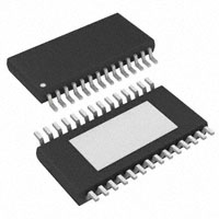
The device is available in a 28-pin TSSOP PowerPAD
package. The PowerPAD package is designed to
transfer heat into the ground plane, eliminating the need
for external heat sinks—minimizing solution cost and size.
D Multimedia Speakers
D Notebook Computers
VCC = 12V
0.47 µF
RIN1+
From TV
From CD
Player
From TV
From CD
Player
RIN2+
R
0.47 µF
RIN1−
RIN2−
Depop
Circuitry
From DAC or
PVcc
PVcc
Vcc
Mux
Input Mux
Management
Control
SEDIFF
32−Step
(DC Voltage)
SEMAX
Volume
Control
0.47 µF
LIN1+
LIN2+
Output Mode
Control
From CD
Player
1 kΩ
Shutdown
5VREF
To Potentiometers
or DAC reference
SE/BTL
1 kΩ
220 µF
100 kΩ
L
Mux
47 nF
VCC/2
0.47 µF
0.47 µF
Bypass
System
Control
Potentiometers
0.47 µF
220 µF
100 kΩ
Gnd
VOLUME
From TV
16 Ω
Rout −
−
R
CLK
From TV
+
Power
IN2/IN1
Control
Player
VCC/2
10 µF
Rout +
0.47 µF
System
From CD
1 µF
Mux
0.47 µF
LIN1−
L
LIN2−
Mux
+
−
Lout +
Lout −
16 Ω
0.47 µF
Please be aware that an important notice concerning availability, standard warranty, and use in critical applications of Texas Instruments
semiconductor products and disclaimers thereto appears at the end of this data sheet.
PowerPAD is a trademark of Texas Instruments.
PRODUCTION DATA information is current as of publication date. Products
conform to specifications per the terms of Texas Instruments standard warranty.
Production processing does not necessarily include testing of all parameters.
Copyright 2003, Texas Instruments Incorporated
�TPA6030A4
www.ti.com
SLOS395B − DECEMBER 2002 − REVISED JANUARY 2005
These devices have limited built-in ESD protection. The
leads should be shorted together or the device placed in
conductive foam during storage or handling to prevent
electrostatic damage to the MOS gates.
ORDERING INFORMATION
SPECIFIED TEMPERATURE
RANGE
PACKAGE DEVICE
TSSOP (PWP)
−40°C to 85°C
TPA6030A4PWP
CAUTION:
During normal operation, shorting the outputs together, to
ground, or to VCC may cause permanent damage to the
device.
(1)
The PWP package is available taped and reeled To order a taped
and reeled part, add the suffix R to the part number (e.g.,
TPA6030A4PWPR).
PACKAGE DISSIPATION RATINGS
PACKAGE
TA ≤ 25°C POWER
RATING
DERATING FACTOR
ABOVE TA = 25°C
TA = 70°C POWER
RATING
TA = 85°C POWER
RATING
PWP
4.47W(1)
35.8 mW/°C
2.86 W
2.32 W
(1)
The PowerPAD must be soldered to a thermal land on the printed-circuit board. Refer to the Texas Instruments
document, PowerPAD Thermally Enhanced Package Application Report (literature number SLMA002) for more
information on the PowerPAD package. The thermal data was measured on a PCB layout based on the information in
the section entitled Texas Instruments Recommended Board for PowerPAD on page 33 of the before mentioned
document.
ABSOLUTE MAXIMUM RATINGS
over operating free-air temperature range unless otherwise noted(1)
TPA6030A4
Supply voltage, VCC, PVCC
−0.3 V to 15 V
IN2, IN1 Input voltage, VI
−0.3 V to VCC + 0.3V
Continuous total power dissipation
See Dissipation Rating Table
Operating free-air temperature range, TA
−40°C to 85°C
Operating junction temperature range, TJ
−40°C to 150°C
Storage temperature range, Tstg
−65°C to 85°C
Lead temperature 1,6 mm (1/16 inch) from case for 10 seconds
(1)
260°C
Stresses beyond those listed under “absolute maximum ratings” may cause permanent damage to the device. These are stress ratings only, and
functional operation of the device at these or any other conditions beyond those indicated under “recommended operating conditions” is not
implied. Exposure to absolute-maximum-rated conditions for extended periods may affect device reliability.
RECOMMENDED OPERATING CONDITIONS
MIN
MAX
7
15
0.8VCC
VCC
SHUTDOWN
2
VCC
SE/BTL, IN2/IN1
0
0.5 VCC
SHUTDOWN
0
0.8
−40
85
Supply voltage, PVCC, VCC
High input voltage,
voltage VIH
Low input voltage,
voltage VIL
Operating free-air temperature, TA
2
SE/BTL, IN2/IN1
UNIT
V
V
V
°C
�TPA6030A4
www.ti.com
SLOS395B − DECEMBER 2002 − REVISED JANUARY 2005
ELECTRICAL CHARACTERISTICS
TA = 25°C, VCC = PVCC = 12 V, unless otherwise noted
PARAMETER
| VOS |
TEST CONDITIONS
Volume
V
l
= 36 dB,
dB
SE/BTL = 0 V
Output offset
PSRR
Power supply rejection ratio
|IIH|
High level input current
High-level
|IIL|
Low level input current
Low-level
ICC
ICC(SD)
MAX
10
55
Out+ to V(BYPASS)
10
105
Out− to V(BYPASS)
10
105
−42
VCC = 15 V, VI = VCC
1
3
SE/BTL, IN2/IN1
VCC = 15 V, V I = 12 V
VCC = 15 V, VI = 0
SHUTDOWN,
VCC = 15 V, VI = 0
1
18
26
SE/BTL = VCC,
VCC = 7 V to 15 V
11
16
SE/BTL = 0 V,
SHUTDOWN = VCC
Supply current, shutdown
mode
No Load,
VCC=15 V,
SHUTDOWN = 0.8 V
VCC = 7 V to 15 V,
VOMAX
RL =16 Ω, VOLUME = 5VREF,
IN+ = (VCC / 2) − 1 V and
IN− = (VCC / 2) + 1 V
OR
IN+ = (VCC / 2) + 1 V and
IN− = (VCC / 2) − 1 V
1
SE/BTL = 0 V,
VCC = 7 V to 15 V
RL =16 Ω,
RL = 16-Ω stereo,
Pin floating
mV
µA
A
µA
A
mA
1.2
4.4
VCC = 7 V
VCC = 12 V
UNIT
dB
SHUTDOWN,
Supply current, full clipping
at outputs, stereo operation
DC maximum output voltage
swing per output(1)
−60
SE/BTL, IN2/IN1
5VREF
(1)
MIN
VCC = PVCC = 12 V to 15 V
No load,
SHUTDOWN = 2 V
Supply current
TYP
Out+ to Out−
A
1
3
4.7
5.5
V
9.3
VPP
µA
4.4
7.6
VCC = 15 V
8.4
9.8
See diagram below
DC MAXIMUM OUTPUT VOLTAGE SWING PER CHANNEL
VCC
VOMAX
Rout+
Voltage Drop.
Typically Referred
To As VOH
Voltage Drop.
Typically Referred
To As VOL
RL = 16 Ω
VCC
Rout−
VOMAX
3
�TPA6030A4
www.ti.com
SLOS395B − DECEMBER 2002 − REVISED JANUARY 2005
OPERATING CHARACTERISTICS
TA = 25°C, RL = 16 Ω, Volume = 8.13 dB, unless otherwise noted3
TEST CONDITIONS
PARAMETER
THD=1%,
VCC = 12 V
PO
MIN
f = 1 kHz
THD=10%, f = 1 kHz
Output power
3
4(1,2)
THD=10%, f = 1 kHz
5(1,2)
0.1%
THD+N
Total harmonic distortion plus noise
PO = 1 W,
f = 20 Hz to 20 kHz
BOM
Maximum output power bandwidth
THD+N < 10%
VCC = 7 V to 15 V
−58
Supply ripple rejection ratio
f = 20 Hz−20 kHz,
C(BYPASS) = 1 µF,
V(ripple) = 100 mVrms, BTL
VCC = 7 V
kSVR
VCC = 12 V
−60
VCC = 15 V
−60
Channel to channel output separation
f = 1 kHz,
Volume = 0.53 dB
−110
Volume = 0.53 dB
102.5
Signal to noise ratio
Signal-to-noise
f = 20 Hz to 20 kHz,
BTL, Inputs ac grounded,
THD+N = 0.5%,
PO = 2.35 W
Xtalk
SNR
Attenuation, input to output in shutdown
mode
BTL,
MAX
UNIT
2.2
f = 1 kHz
THD=1%,
VCC = 15 V
TYP
20
W
kHz
dB
dB
dBV
Volume = 36 dB
83
SE, f = 20 Hz−20 kHz, RL = 32 Ω, Volume = 30 dB
73
BTL, f = 20 Hz−20 kHz, RL = 16 Ω, Volume = 36 dB
110
dB
(1)
At TA = 25°C, a derating factor of 48 mW/°C is necessary in order for the device to function properly in this configuration.
(2)
If used on a board with a layout set forth on page 33 of the PowerPAD Thermally Enhanced Package Application Report (literature number
SLMA002) to achieve a derating factor of 35.8mW/°C, it is possible to operate the device at these output power levels so long as it is in a mono,
BTL configuration.
4
�TPA6030A4
www.ti.com
SLOS395B − DECEMBER 2002 − REVISED JANUARY 2005
PIN ASSIGNMENTS
PWP PACKAGE
(TOP VIEW)
ROUT−
PVCC
SEMAX
RIN1−
RIN1+
RIN2−
RIN2+
VCC
LIN1−
LIN1+
LIN2−
LIN2+
NC
LOUT−
1
2
3
4
5
6
7
8
9
10
11
12
13
14
28
27
26
25
24
23
22
21
20
19
18
17
16
15
GND
ROUT+
SE/BTL
IN2/IN1
SHUTDOWN
VOLUME
SEDIFF
5VREF
CLK
GND
BYPASS
PVCC
LOUT+
GND
NC − No internal connection
Terminal Functions
TERMINAL
I/O
DESCRIPTION
NAME
NO.
5VREF
21
O
Internal 5-V reference for VOLUME, SEDIFF, and SEMAX pins ONLY
BYPASS
18
I
Connect capacitor to ground for BYPASS midrail voltage supply filtering
CLK
20
I
Connect capacitor to ground to set clock frequency of volume control counter
GND
15, 19, 28
I
Ground
IN2/IN1
25
I
Controls input MUX, high selects IN2 inputs, low selects IN1 inputs
LIN1−
9
I
Left negative differential input, selected when IN2/IN1 is held low
LIN1+
10
I
Left positive differential input, selected when IN2/IN1 is held low
LIN2−
11
I
Left negative differential input, selected when IN2/IN1 is held high
LIN2+
12
I
Left positive differential input, selected when IN2/IN1 is held high
LOUT−
14
O
Left negative output in speaker mode and high impedance in headphone mode
LOUT+
16
I
Left positive output in speaker mode, and positive output in headphone mode
NC
13
No internal connection
PVCC
2,17
I
Power supply for the output stage
RIN1−
4
I
Right negative differential input, selected when IN2/IN1 is held low
RIN1+
5
I
Right positive differential input, selected when IN2/IN1 is held low
RIN2−
6
I
Right negative differential input, selected when IN2/IN1 is held high
RIN2+
7
I
Right positive differential input, selected when IN2/IN1 is held high
ROUT+
27
O
Right positive output in speaker mode, and positive output in headphone mode
ROUT−
1
O
Right negative output in speaker mode (BTL) and high impedance in headphone mode (SE)
SE/BTL
26
I
Determines output mode, high selects headphone mode (SE), low selects speaker mode (BTL)
SEDIFF
22
I
Sets the difference between speaker and headphone volume (from –6 dB down to mute)
SEMAX
3
I
Sets maximum headphone volume. DC range is 0 to 5VREF
SHUTDOWN
24
I
Shutdown terminal (active low, TTL compatible, VCC compliant)
VCC
8
I
Supply voltage terminal
VOLUME
23
I
Master volume control. DC voltage range is 0 to 5VREF
THERMAL PAD
−
−
Connect to ground. The thermal pad must be soldered down in all applications to properly secure the
device on the PC board. Properly soldering the thermal pad to the PC board is necessary for achieving
the required heat transfer for device cooling.
5
�TPA6030A4
www.ti.com
SLOS395B − DECEMBER 2002 − REVISED JANUARY 2005
VOLUME CONTROL
Table 1 shows the functionality of the 32-step volume control. The voltage difference between trip levels is 2.66% of 5VREF,
and the difference between gain steps is 2.53 dB.
Table 1. Volume Control
(VCC = 12 V, No Load, SEDIFF = 0 V, SEMAX = 5VREF)
VOLTAGE ON VOLUME PIN AS A
PERCENTAGE OF 5VREF
SPEAKER VOLUME
(dB)
HEADPHONE VOLUME
(dB)
0−10
−80.00
−86.00
10−12.6
−40.00
−46.00
12.6−15.2
−37.47
−43.47
15.2−18
−34.93
−40.93
18−20.6
−32.40
−38.40
20.6−23.4
−29.87
−35.87
23.4−26
−27.33
−33.33
26−28.6
−24.80
−30.80
28.6−31.4
−22.27
−28.27
31.4−34
−19.73
−25.73
34−36.6
−17.20
−23.20
36.6−39.4
−14.67
−20.67
39.4−42
−12.13
−18.13
42−44.6
−9.60
−15.60
44.6−47.2
−7.07
−13.07
47.2−50
−4.53
−10.53
50−52.6
−2.00
−8.00
52.6−55.4
0.53
−5.47
55.4−58
3.07
−2.93
58−60.6
5.60
−0.40
60.6−63.4
8.13
2.13
63.4−66
10.67
4.67
66−68.6
13.20
7.20
68.6−71.4
15.73
9.73
71.4−74
18.27
12.27
74−76.6
20.80
14.80
76.6−79.4
23.33
17.33
79.4−82
25.87
19.87
82−84.6
28.40
22.40
84.6−87.4
30.93
24.93
87.4−90
33.47
27.47
90−100
36.00
30.00
Refer to the section entitled Volume Control Description in the Application Information section of this data sheet for more
details regarding the use of the volume control.
6
�TPA6030A4
www.ti.com
SLOS395B − DECEMBER 2002 − REVISED JANUARY 2005
The volume in single-ended (SE) mode is determined by the following equation:
SE Volume + min [(VOLUME * SEDIFF) or (SEMAX)]*6 dB, where VOLUME is the voltage (expressed in terms
of %VREF) applied to the VOLUME pin, SEDIFF is the voltage (%VREF) applied to the SEDIFF pin, and SEMAX is the
voltage (%VREF) applied to the SEMAX pin. The SE Volume control is integrated into the 32-step volume control. A block
diagram of the SE Volume control portion is shown in Figure 1.
+
VOLUME
SEDIFF
+
Control
−
SEMAX
To Next Stage of
32-Step Volume
Control
2:1 Mux
VOLUME−SEDIFF
SEMAX
Figure 1. Block Diagram of the SE Volume Control
Refer to the section entitled Volume Control Description in the Application Information section of this data sheet for more
details regarding the use of the volume control.
VOLUME CONTROL
40
30
Headphone Volume With
SEMAX Set to 5VREF
20
10
Volume − dB
0
Speaker Volume
−10
Headphone Volume With
SEMAX Set to 7.2 dB
−20
−30
−40
−50
−60
SEDIFF = 0 V
−70
−80
−90
0
10
20
30
40
50
60
%5VREF
70
80
90
100
Figure 2. Speakers (BTL) and Headphones (SE) Volume vs %5VREF
Figure 2 illustrates the functionality of the TPA6030A4 volume control. As the voltage applied to the VOLUME control pin
is increased, the volume increases.
Increasing the voltage on the SEDIFF pin increases the delta in volume between speaker (BTL) and headphone (SE)
volume from a minimum of 6 dB to a maximum reduction in headphone volume, resulting in mute.
The SEMAX input limits the maximum output level in headphone mode. The dashed line shows operation with SEMAX
set to 5VREF, which results in maximum output in headphone mode. The horizontal line in Figure 2 shows operation with
SEDIFF set to 0V, and SEMAX set to 67.3% of 5VREF, for a maximum volume in headphone mode of 7.2 dB.
Neither SEMAX nor SEDIFF have any affect on the volume in speaker mode.
7
�TPA6030A4
www.ti.com
SLOS395B − DECEMBER 2002 − REVISED JANUARY 2005
TYPICAL CHARACTERISTICS
TABLE OF GRAPHS
FIGURE
THD+N
Total harmonic distortion plus noise (BTL)
THD+N
Total harmonic distortion plus noise (SE)
Crosstalk (BTL)
CMRR
Common mode rejection ratio
vs Output power
3
vs Frequency
5
vs Output power
4
vs Frequency
6
vs Frequency
7
vs Frequency
8
9
Closed loop response (BTL)
vs Frequency
10
PD
Power dissipation
vs Output power (per channel)
11
Ri
Input resistance
vs Volume
12
RL
Recommended load impedance
vs Supply voltage
13
THD + N − Total Harmonic Distortion + Noise (BTL) − %
TOTAL HARMONIC DISTORTION + NOISE (BTL)
vs
OUTPUT POWER
100
VCC = 12 V,
RL = 16 Ω,
f = 1 kHz
10
1
Volume = 8.13 dB
0.1
0.01
0.1
0.5
1
PO − Output power − W
Figure 3
8
2
3
THD + N − Toatal Harmonic Distortion + Noise (SE) − %
vs Common-mode input voltage
TOTAL HARMONIC DISTORTION + NOISE (SE)
vs
OUTPUT POWER
100
VCC = 12 V
RL = 32 Ω
f = 1 kHz
10
1
Volume = −0.4 dB
0.1
0.01
10
50
100
PO − Output power − mW
Figure 4
200
300 400
�TPA6030A4
www.ti.com
SLOS395B − DECEMBER 2002 − REVISED JANUARY 2005
1
VCC = 12 V
RL = 16 Ω
PO = 1 W
Volume = 0.53 dB
0.1
PO = 2 W
Volume = 3.07 dB
0.01
20
100
1k
f − Frequency − Hz
10 k 20 k
TOTAL HARMONIC DISTORTION + NOISE (SE)
vs
FREQUENCY
THD + N − Toatal Harmonic Distortion + Noise (SE) − %
THD + N − Total Harmonic Distortion + Noise (BTL) − %
TOTAL HARMONIC DISTORTION + NOISE (BTL)
vs
FREQUENCY
1
VCC = 12 V
RL = 32 Ω
PO = 100 mW
Volume = −0.4 dB
0.1
0.01
20
100
Figure 5
COMMON-MODE REJECTION RATIO
vs
FREQUENCY
−30
VCC = 12 V,
RL = 16 Ω,
Volume = 0.53 dB
CMRR − Common-Mode Rejection Ratio − dB
Crosstalk − dB
−90
−100
−110
−120
−130
−140
−150
20
100
1k
f − Frequency − Hz
Figure 7
10 k 20 k
Figure 6
CROSSTALK (BTL)
vs
FREQUENCY
−80
1k
f − Frequency − Hz
10 k 20 k
−40
VI = 1 Vrms,
VCC = 12 V,
CI = 0.47 µF
RL = 16 Ω, BTL
Volume = 0.53 dB
−50
−60
RL = 32 Ω, SE
Volume = −0.4 dB,
CO = 100 µF
−70
−80
−90
−100
20
100
1k
f − Frequency − Hz
10 k 20 k
Figure 8
9
�TPA6030A4
www.ti.com
SLOS395B − DECEMBER 2002 − REVISED JANUARY 2005
COMMON-MODE REJECTION RATIO
vs
COMMON-MODE INPUT VOLTAGE
40
VCC = 15 V,
f = 1 kHz,
CI = 0.47 µF
−10
35
Volume − dB
−20
−30
−40
Volume = 0.53 dB,
16 Ω BTL
Volume = 0.4 dB,
32 Ω SE, CO = 100 µF
25
20
VCC = 12 V,
PO = 2 W BTL,
RL = 16 Ω
15
5
0
5
10
VIC − Common-Mode Input Voltage − VPP
15
−250°
0
10
100
1k
f − Frequency − Hz
900
Ri − Input Resistance − k Ω
VCC = 15 V
VCC = 12 V
1.5
VCC = 7 V
1
700
600
500
400
300
200
0.5
0
VCC = 12 V,
BTL Configuration,
16 Ω Load
800
2.5
2
100 k
INPUT RESISTANCE
vs
VOLUME
3.5
RL = 16 Ω
Mono Operation
3 BTL
10 k
Figure 10
POWER DISSIPATION
vs
OUTPUT POWER (PER CHANNEL)
PD − Power Dissipation − W
−150°
−200°
Phase, CI = 470 µF
Figure 9
100
0
1
2
3
4
PO − Output Power (Per Channel) − W
Figure 11
10
−50°
−100°
Phase, CI = 0.47 µF
10
−60
−70
Volume = 36 dB, CI = 0.47 µF
30
−50
0
Volume = 36 dB, CI = 470 µF
5
0
−40
−20
0
Volume − dB
Figure 12
20
40
φ − Phase − Degrees
0
CMRR − Common-Mode Rejection Ratio − dB
CLOSED LOOP RESPONSE (BTL)
vs
FREQUENCY
�TPA6030A4
www.ti.com
RL− Recommended Minimum Load Impedance (Per Channel) − Ω
SLOS395B − DECEMBER 2002 − REVISED JANUARY 2005
RECOMMENDED LOAD IMPEDANCE
vs
SUPPLY VOLTAGE
25
Derating Factor = 35.8 mW/°C,
TA = 25°C, TJMax = 150°C,
BTL Configuration,
Stereo Operation
20
15
10
5
0
7
8
10
11
12
13
9
VCC − Supply Voltage − V
14
15
Figure 13
11
�TPA6030A4
www.ti.com
SLOS395B − DECEMBER 2002 − REVISED JANUARY 2005
APPLICATION INFORMATION
VOLUME, SEDIFF, AND SEMAX OPERATION
The three pins labeled VOLUME, SEDIFF, and SEMAX control the speaker (BTL) volume (VOLUME pin only) and the
headphone (SE) volume. All three of these pins are controlled with a dc voltage. These voltages are a percentage of the
voltage on the 5VREF pin. The 5VREF pin sources up to 5 mA when VCC = 12 V. It is specifically designed to be a reference
voltage supply for the volume control that can be used with analog-to-digital converters (ADCs), resistor divider networks,
and potentiometers.
When driving in BTL mode, the VOLUME pin is the only pin that controls the volume. Table 1 shows the different volumes
and the corresponding voltages applied to the VOLUME pin. When driving in SE mode, all three pins can be used to control
the volume. Table 2 shows the different headphone volumes and the corresponding voltages applied to each pin.
The TPA6030A4 allows the user to specify a difference between the BTL volume and the SE volume. This is desirable
because it allows the user to avoid any listening discomfort when plugging in headphones. The volume in headphone mode
is proportional to that in speaker mode, and is no less than 6 dB lower (refer to the section labeled bridge−tied load versus
single-ended load for an explanation).
The SEDIFF and SEMAX pins control the difference in volume between speaker and headphone modes. As the voltage
on the SEDIFF pin is increased, the difference between the BTL and SE volumes is also increased. Applying a lower voltage
on the SEDIFF pin decreases the volume difference. So, for example, if the speaker volume was set to 36 dB, and SEMAX
was set to 5VREF, one could vary SEDIFF to get a headphone volume from as much as 30 dB to as little as –86 dB, or
mute.
The SEMAX pin can be used to set the maximum possible headphone volume. The greater the voltage applied to this pin,
the higher the maximum volume. If the voltage reaches 5VREF, any volume level set by the VOLUME and SEDIFF pins
passes on through to the headphones. Should the voltage on SEMAX go to 0 V, the headphones would be muted,
regardless of what voltage is applied to the VOLUME and SEDIFF pins. The level set by the SEMAX pin does not affect
headphone volumes below that maximum level. Table 2 shows examples of how these pins interact with each other.
+
VOLUME
SEDIFF
+
Control
−
SEMAX
To Next Stage of
32-Step Volume
Control
2:1 Mux
VOLUME−SEDIFF
SEMAX
Figure 14. Block Diagram of the SE Volume Control
Table 2. Assorted Headphone and Speaker Volume Configurations
MODE
VOLTAGE ON
VOLUME PIN
(%5VREF)
VOLTAGE ON
SEDIFF PIN
(%5VREF)
VOLTAGE ON
SEMAX PIN
(%5VREF)
HP
100
0
HP
0
0
HP
100
100
HP
60
0
HP
100
40
HP
100
40
Speaker
60
Speaker
Speaker
X = Don’t care
12
HEADPHONE
VOLUME
dB
SPEAKER
VOLUME
dB
100
30
N/A
100
−86
N/A
0
−86
N/A
100
2.13
N/A
40
−18.13
N/A
80
2.13
N/A
0
100
N/A
8.13
100
X
X
N/A
36
0
X
X
N/A
−80
�TPA6030A4
www.ti.com
SLOS395B − DECEMBER 2002 − REVISED JANUARY 2005
CLOCK PIN
The TPA6030A4 has an internal clock whose frequency is controlled by the value of an external capacitor on pin 20. The
relationship between the capacitor and the clock frequency is seen in Figure 15.
The clock plays a pivotal role in the functionality of the TPA6030A4. It determines how quickly the volume can change.
When a voltage is applied to the VOLUME pin (or if in SE mode, the SEDIFF or SEMAX pins as well), it causes a change
in volume. The volume does not change instantaneously. It moves one step for every sixteen clock cycles. For example,
if the volume is initially at 36 dB in BTL mode, and then a voltage is applied to the VOLUME pin to set the volume to 0.53 dB,
the volume decreases by 14 steps. With a 47-nF capacitor connected to the clock pin, the clock frequency is 390 Hz. The
time it takes for the volume to reach the desired level is 574 ms. See equation 1.
Total time + # of Volume Steps
16
ǒClock Frequency
Ǔ
(1)
Figure 16 demonstrates how the volume changes with respect to the clock cycles, and how the frequency of the clock
affects the time necessary for each step. The triangular waveform is the voltage on the clock pin, and in this case, the clock
frequency is 390 Hz. Each volume step takes 41 ms, which is consistent with equation 1.
f − Frequency − Hz
10 k
1k
400
100
1
10
50
Clock Capacitor − nF
100
Figure 15. Clock Frequency vs Capacitance on Clock Pin
Figure 16. How the Volume Changes With Respect to the Clock
13
�TPA6030A4
www.ti.com
SLOS395B − DECEMBER 2002 − REVISED JANUARY 2005
SHUTDOWN
The shutdown function of the TPA6030A4 is designed to bring all the outputs and the BYPASS pin to dc ground. The output
transistors are turned off, and the current consumption of the device drops to less than 3 µA.
In order for the part to go into shutdown, the SHUTDOWN pin must be held at a logic low (0.8 V to 0 V). Once the
SHUTDOWN pin is held at a logic low, the volume must ramp down to mute. The device goes through each volume step
until the output is muted. That is why it takes longer for the device to shut down at higher volume levels (see Figures 17,
18, and 21). The device has to go through more steps. Once the volume is muted, the dc voltage of the outputs go to ground.
The time it takes for this stage of the shutdown process is proportional to the size of the BYPASS capacitor. The smaller
the capacitor, the more quickly the device shuts down. See Figure 21. However, making the BYPASS capacitor too small
likely results in unwanted pop. The recommended range of values are between 0.1 µF to 1 µF.
The start-up time, however, is not dependent upon the volume level. Figures 19 and 20 show that the start-up time for the
TPA6030A4 is not dependent upon the volume level. When the SHUTDOWN pin is held at a logic high (2 V to VCC), the
dc level of the outputs begin to increase. At the same time, the volume control is ramping up until it reaches the desired
volume level.
500 ms/div
Figure 17. Shutdown Curve When the
Volume = 0.53 dB
14
Figure 18. Shutdown Curve When the
Volume = 36 dB
�TPA6030A4
www.ti.com
SLOS395B − DECEMBER 2002 − REVISED JANUARY 2005
Figure 19. Start-Up Curve When the
Volume = 0.53 dB
Figure 20. Start-Up Curve When the
Volume = 36 dB
SHUTDOWN TIME
vs
BYPASS CAPACITANCE
3.5
RL = 16 Ω
BTL
t − Shutdown Time − s
3
Volume = 36 dB
2.5
2
Volume = 0.53 dB
1.5
1
0.5
0
0
0.2
0.4
0.6
0.8
Bypass Capacitance − µF
1
1.2
Figure 21. Shutdown Time vs Bypass Capacitance
15
�TPA6030A4
www.ti.com
SLOS395B − DECEMBER 2002 − REVISED JANUARY 2005
APPLICATION CIRCUIT
Application circuit using the TPA6030A4 in an LCD monitor with headphone outputs and volume control.
VCC
+
C13
10 µF
C11
1 µF
+
R6
100 kΩ
R5
C14
220 µF
1 kΩ
R7
100 kΩ
R8
33 kΩ
SEMAX
C15
1 µF
R9
68 kΩ
1 kΩ
R4
RIN1−
RIN1+
RIN2−
RIN2+
LIN1−
LIN1+
LIN2−
LIN2+
C1
VOLUME
0.47 µF
R1 100 kΩ
TPA6030A4PWP
C2
0.47 µF
C3
0.47 µF
C4
0.47 µF
C5
C6
C7
C8
0.47 µF
0.47 µF
0.47 µF
0.47 µF
1
2
3
4
5
6
7
8
9
10
11
12
13
14
Rout −
PVcc
SEMAX
RIN1−
RIN1+
RIN2−
RIN2+
Vcc
LIN1−
LIN1+
LIN2−
LIN2+
NC
Lout −
GND
Rout +
SE/BTL
IN2/IN1
SHUTDOWN
VOLUME
SEDIFF
5VREG
CLK
GND
BYPASS
PVcc
Lout +
GND
28
27
26
25
24
23
R2
82 kΩ
+
C12
220 µF
R2 SEDIFF
18 kΩ
System
Control
22
21
20
19
18
17
16
C10
47 nF
+
15
C9
0.47 µF
C13
1 µF
VCC
C11
10 µF
Figure 22. Typical Application Circuit for an LCD Monitor
Volume Control Description
The circuit shown in Figure 22 automatically switches between headphone outputs and speaker outputs when a
headphone plug is inserted or removed from the headphone jack. Additionally, this circuit uses resistor divider networks
to limit the headphone volume. Resistors R8 and R9 form a divider network that applies 67% of 5VREF to the SEMAX
pin, which results in a maximum output of 7.2 dB. Resistors R2 and R3 form a divider network that applies 18% of 5VREF
to the SEDIFF pin.
16
�TPA6030A4
www.ti.com
SLOS395B − DECEMBER 2002 − REVISED JANUARY 2005
The effect of the resistor dividers can be observed when the output is switched from speaker to headphone mode. If the
voltage on the volume pin is greater than 85% of 5VREF, the resistor divider network around SEMAX limits the headphone
volume to 7.2 dB. If the voltage on the VOLUME pin falls below 85% of 5VREF, SEDIFF limits the headphone volume to
13.6 dB less than the speaker volume. To convert a percentage of 5VREF to volume in dB, refer to the column in Table
1 labeled %5VREF, and find the corresponding speaker volume. That value can then be substituted into the following
equations for VOLUME, SEDIFF, or SEMAX. It is important, however, to find the minimum based on the %5VREF before
converting to dB.
SE Volume + min ƪ(VOLUME * SEDIFF) or (SEMAX)ƫ*6 dB
(2)
When the voltage on the VOLUME pin is > 85% of 5VREF, or at 90% of 5VREF for example, the headphone volume is
determined by the following equation:
SE Volume + min ƪ(90%5VREF * 18%5VREF) or (67%5VREF)ƫ*6 dB +
67%5VREF * 6dB + 13.2 dB*6 dB + 7.2 dB
(3)
When the voltage on the VOLUME pin is < 85% of 5VREF, or at 50% of 5VREF for example, the headphone volume is
determined by the following equation:
SE volume + min ƪ(50%5VREF * 18%5VREF) or (67%5VREF)ƫ*6 dB +
32%5VREF*6 dB + *19.73 dB*6 dB + *25.73 dB
(4)
When the voltage on the VOLUME pin = 85% of 5VREF, both SEMAX and SEDIFF have the same affect on the headphone
volume.
SE Volume + min ƪ(85%5VREF * 18%5VREF) or (67%5VREF)ƫ*6 dB +
67%5VREF*6 dB + 13.2 dB*6 dB + 7.2 dB
(5)
–46 dB is the lowest the SE volume can go without going into mute. So, for example, if the end calculation for the SE volume
was –50 dB, the actual volume would be mute.
It is important to note that the evaluation module (EVM) for the TPA6030A4, SLOP365, does not have fixed resistors for
setting the voltages on the VOLUME, SEDIFF, and SEMAX pins. It has potentiometers in place of the resistor divider
networks for added flexibility. Potentiometers may be used in an application as well.
Another method of controlling the voltage on the SEDIFF and SEMAX pins would be to apply the voltage with an external
controller, using 5VREF as a reference voltage.
Input Capacitor, CI
The input capacitor allows the amplifier to bias the input signal to the proper dc level for proper operation. In this case, the
input capacitor, CI, and the input impedance of the amplifier, RI, form a high-pass filter with the corner frequency determined
in equation 6. Figure 23 shows how the input capacitor and the input resistor within the amplifier interact.
Rf
CI
Input Signal
IN
RI
Figure 23. Input Resistor and Input Capacitor
17
�TPA6030A4
www.ti.com
SLOS395B − DECEMBER 2002 − REVISED JANUARY 2005
−3 dB
f
c(highpass)
+
1
2pR C
I I
(6)
fc
The value of CI is important to consider as it directly affects the low frequency, or bass, performance of the circuit.
Futhermore, the input impedance changes with a change in volume. The higher the volume, the lower the input impedance.
To determine the appropriate capacitor value, reconfigure equation 6 into equation 7. The value of the input resistor, RI,
can be determined from Figure 12.
CI +
1
2pRI f c
(7)
Low leakage tantalum or ceramic capacitors are recommended. When polarized capacitors are used, the positive side of
the capacitor should face the amplifier input in most applications as the dc level there is held at VCC/2, which is likely higher
than the source dc level. Note that it is important to confirm the capacitor polarity in each specific application.
Recommended capacitor values are between 0.1 µF and 1 µF.
Power Supply Decoupling, CS
The TPA6030A4 is a high-performance audio amplifier that requires adequate power supply decoupling to ensure the
output total harmonic distortion (THD) is as low as possible. Power supply decoupling also prevents oscillations for long
lead lengths between the amplifier and the speaker. The optimum decoupling is achieved by using two capacitors of
different types to reduce different types of noise on the power supply leads. For higher frequency transients, spikes, or
digital noise on the power supply, a good low equivalent-series-resistance (ESR) ceramic capacitor, typically 0.1 µF, should
be placed as close as possible to the device VCC pin. For filtering lower frequency noise signals, a larger aluminum
electrolytic capacitor of 10 µF or greater should be placed near the audio power amplifier.
Midrail Bypass Capacitor, C(BYPASS)
The midrail bypass capacitor, C(BYPASS), has several important functions. During start-up or recovery from shutdown mode,
C(BYPASS) determines the rate at which the amplifier starts up. C(BYPASS) also reduces noise coupled into the output signal
by the power supply. Generally, ceramic or tantalum low-ESR capacitors with values ranging from 0.1 µF to 1.0 µF are
recommended for the best THD and noise performance.
Output Coupling Capacitor, CC
In a typical single-supply SE configuration, an output coupling capacitor, CC, is required to block the dc bias at the output
of the amplifier, thus preventing dc currents from flowing through the load. This in turn reduces the current draw of the
amplifier significantly. As with the input coupling capacitor, the output coupling capacitor and impedance of the load form
a high pass filter governed by equation 8.
−3 dB
f
c(highpass)
+
1
2pR C
L C
(8)
fc
18
�TPA6030A4
www.ti.com
SLOS395B − DECEMBER 2002 − REVISED JANUARY 2005
Large values of CC are required to pass low frequencies to the load. Consider an example where CC is 220 µF, and the
load varies from 16 Ω, 32 Ω, 10 kΩ, and 47 kΩ. Table 3 summarizes the frequency response characteristics of each of the
preceding configurations.
Table 3. Load Impedances vs Low Frequency Characteristics in SE Mode
RL
(Ω)
CC
(µF)
LOWEST FREQUENCY
(Hz)
16
220
45
32
220
23
10k
220
0.07
47k
220
0.015
Using Low-ESR Capacitors
Low-ESR capacitors are recommended throughout this applications section. A real (as opposed to ideal) capacitor can
be modeled simply as a resistor in series with an ideal capacitor. The voltage drop across the resistor minimizes the
beneficial effects of the capacitor in the circuit. The lower the equivalent value of this resistance, the more the real capacitor
behaves like an ideal capacitor.
Bridge-Tied Load Versus Single-Ended Mode
Figure 24 shows a Class-AB audio power amplifier (APA) in a bridge-tied-load (BTL) configuration. The TPA6030A4
amplifier consists of two Class-AB differential amplifiers driving both the positive and negative terminals of the load (per
channel). Specifically, differential drive means that as one side amplifier (the positive terminal, for example) is slewing up,
the other side is slewing down, and vice versa. This doubles the voltage swing across the load as opposed to a
ground-referenced load, or a single-ended load. Power is proportional to the square of the voltage. Plugging 2x VO(PP) into
the power equation yields 4X the output power from the same supply rail and load impedance as would have been obtained
with a ground referenced load (see equation 9).
V
(RMS)
+
Power +
V
(9)
O(PP)
2 Ǹ2
V
(RMS)
R
L
2
VCC
VO(PP)
2x VO(PP)
VCC
−VO(PP)
Figure 24. Bridge-Tied-Load Configuration
19
�TPA6030A4
www.ti.com
SLOS395B − DECEMBER 2002 − REVISED JANUARY 2005
VCC
−3 dB
VO(PP)
CC
RL
VO(PP)
fc
Figure 25. Single-Ended Configuration and Frequency Response
Bridge-tying the outputs in a typical computer audio, or LCD TV or multimedia LCD monitor application drastically increases
output power. For example, if an amplifier in a single-ended configuration was capable of outputting a maximum of 250 mW
for a given load with a supply voltage of 12 V, then that same amplifier would be able to output 1 W of power in a BTL
configuration with the same supply voltage and load. In addition to the increase in output power, the BTL configuration does
not suffer from the same low frequency issues that plague the single-ended configuration. In a BTL configuration, there
is no need for an output capacitor to block dc, so no unwanted filtering occurs. In addition, the BTL configuration saves
money and space, as the dc-blocking capacitors needed for single-ended operation are large and expensive. For example,
with an 8-Ω load in SE operation, the user needs a capacitor of 995 µF to obtain a lower cutoff frequency of 20 Hz. This
capacitor would be very expensive and very large.
Single-Ended Operation
Figure 25 shows a Class-AB audio power amplifier in an SE configuration. In SE mode, the load is driven from the primary
amplifier for each channel (Rout+ and Lout+, terminals 27 and 16 respectively). The amplifier switches from BTL to SE
mode when the SE/BTL pin is held high(1). This puts the negative outputs of the amplifier into a high impedance state, and
reduces the amplifier’s gain according to the voltage applied to SEDIFF and SEMAX.
SE/BTL Operation
The ability of the TPA6030A4 to easily switch between BTL and SE modes is one of its most important cost saving features.
This feature eliminates the requirement for an additional headphone amplifier in applications where internal stereo
speakers are driven in BTL mode but an external headphone must be accommodated. The follower amplifiers that drive
Rout− and Lout− (terminals 1 and 14) are controlled by the SE/BTL input (terminal 26). When SE/BTL is held low(1), the
amplifiers are on and the TPA6030A4 is in the BTL mode. When SE/BTL is held high(1), only the positive output amplifiers
are on. The negative outputs enter a high impedance state, which configures the TPA6030A4 as an SE driver from the
Rout+ and Lout+ outputs (terminals 27 and 16). Control of the SE/BTL input can be from a separate voltage source or, more
typically, from a resistor divider network. See Figure 26 for an example of a resistor divider network.
Using a readily available 1/8-in. (3,5 mm) stereo headphone jack, the control switch is closed when no plug is inserted.
When closed, the parallel combination of R5 and R7 (see Figure 22) pulls the SE/BTL pin low(1), causing the device to
operate in BTL mode. When a plug is inserted, the 1-kΩ resistor is disconnected and the SE/BTL input is pulled high(1).
When the input goes high(1), the negative output amplifiers go into a state of high impedance, essentially open circuiting
the speaker. The positive output amplifiers then drive through the output capacitor (CO) into the headphone jack.
IN2/IN1 Operation
The TPA6030A4 has the ability to switch between the two input sources. Those sources are dubbed IN2 and IN1. There
is no functional difference between the two inputs. Both perform equally well with any audio signal (provided that signal
is within the specified limits set forth earlier in this document). However, only one input at a time is allowed through to the
output. IN2/IN1 (terminal 26) controls which input is allowed into the amplifier. As with SE/BTL, IN2/IN1 can be controlled
by either a separate voltage source or, more typically, from a resistor divider network. See Figure 26 for an example of a
resistor divider network.
(1)
20
Refer to the table entiled Recommended Operating Conditions.
�TPA6030A4
www.ti.com
SLOS395B − DECEMBER 2002 − REVISED JANUARY 2005
Tying the SE/BTL and IN2/IN1 Pins Together
In some applications, it may be desirable to have one input specifically for BTL operation and one input specifically for SE
operation. This is accomplished by tying the SE/BTL and IN2/IN1 pins together and connecting them to a common control
voltage. An example of this type of configuration can be found in Figure 22. The two pins are tied together and are
connected to the resistor divider network. That network is connected to the stereo headphone jack, and is closed when
no plug is inserted. This pulls both the IN2/IN1 and SE/BTL pins low, causing the amplifier to go into BTL mode using the
IN1 (RIN1 and LIN1) inputs. Should a headphone plug be inserted into the headphone jack, both inputs would be pulled
high, and the amplifier would be in SE mode using the IN2 inputs.
To Rout+ and Right
Speaker
VCC
1 kΩ
TPA6030A4PWP
1
2
3
4
5
6
7
8
9
10
11
12
13
14
Rout −
PVcc
SEMAX
RIN1−
RIN1+
RIN2−
RIN2+
Vcc
LIN1−
LIN1+
LIN2−
LIN2+
NC
Lout −
GND
Rout +
SE/BTL
IN2/IN1
SHUTDOWN
VOLUME
SEDIFF
5VREG
CLK
GND
BYPASS
PVcc
Lout +
GND
28
27
26
100 kΩ
100 kΩ
25
24
23
22
21
20
To Lout+ and Left
Speaker
19
18
17
16
15
Figure 26. Resistor Divider Network
21
�TPA6030A4
www.ti.com
SLOS395B − DECEMBER 2002 − REVISED JANUARY 2005
THERMAL INFORMATION
Class-AB amplifiers are inefficient. The primary cause of these inefficiencies is a voltage drop across the output stage
transistors. There are two components of the internal voltage drop. One is the headroom or dc voltage drop that varies
inversely to output power. The second component is due to the sinewave nature of the output. The total voltage drop can
be calculated by subtracting the RMS value of the output voltage from VCC. The internal voltage drop multiplied by the
average value of the supply current, ICCavg, determines the internal power dissipation of the amplifier.
An easy-to-use equation to calculate efficiency starts out as being equal to the ratio of power from the power supply to the
power delivered to the load. To accurately calculate the RMS and average values of power in the load and in the amplifier,
the current and voltage waveform shapes must first be understood (see Figure 27).
VO
V(LRMS)
ICC
ICCavg
Figure 27. Voltage and Current Waveforms for BTL Amplifiers
Although the voltages and currents for SE and BTL are sinusoidal in the load, currents from the supply are very different
between SE and BTL configurations. In an SE application the current waveform is a half-wave rectified waveform, whereas
in BTL it is a full-wave rectified waveform. This means RMS conversion factors are different. Keep in mind that for most
of the waveform both the push and pull transistors are not on at the same time, which supports the fact that each amplifier
in the BTL device only draws current from the supply for half the waveform. The following equations are the basis for
calculating amplifier efficiency:
Efficiency of a BTL amplifier +
where:
PL +
(10)
PL
P SUP
2
2
VLRMS
V
V
, and VLRMS + P , therefore, P L + P per channel
Ǹ2
RL
2RL
P SUP + VCC I CCavg ) VCC I CC(q)
1
and I CCavg + p
where V P +
therefore,
P SUP +
22
ŕ
p
p
VP
V
2VP
sin(t) dt + * P [cos(t)] 0 +
RL
pR L
pR L
0
Ǹ2 PL R L
2 VCC V P
) V CC I CC(q)
pR L
(12)
(11)
PL = Power delivered to load (per channel)
PSUP = Power drawn from power supply
VLRMS = RMS voltage on BTL load
RL = Load resistance
VP = Peak voltage on BTL load
ICCavg = Average current drawn from the
power supply
VCC = Power supply voltage
ηBTL = Efficiency of a BTL amplifier
ηSE = Efficiency of a SE amplifier
�TPA6030A4
www.ti.com
SLOS395B − DECEMBER 2002 − REVISED JANUARY 2005
Equation 12 represents the power drawn from the supply during mono operation. For stereo operation, the first term of
equation 12 is doubled while the second term in the equation, quiescent power, does not change.
Equation 13 represents the power drawn from the supply during stereo operation.
P SUP(stereo) +
4 VCCV P
) V CC ICC(q)
pR L
(13)
Substituting PL and PSUP into equation 10:
h BTL(stereo) +
4VCCVP
pRL
2 PL
+
) V CC I CC(q)
2p P L RL
4VCCV P ) V CC I CC(q) pR L
Note the factor of 2 in the numerator for stereo operation.
Recall that:
VP +
Ǹ2 PL R L
therefore,
h BTL(stereo) +
2p P L
4VCC
ǸR L
Ǹ2P L ) V CC I CC(q) p ǸRL
(14)
For SE operation, the current waveform is halfwave rectified. Therefore, ICCavg must be recalculated.
In an SE system:
I CCavg
1
+ p
p
2 VP
p
VP
V
sin(t) dt + *
[cos(t)] 2 + P
RL
pR L
p RL
0
0
ŕ
(15)
therefore,
P SUP +
VCCV P
) V CC I CC(q)
p RL
(16)
Stereo operation has the same effect in SE as it does in BTL when doubling the first term of the equation dealing with power
drawn from the supply (equation 16).
P SUP(stereo) +
(17)
2 VCCV P
) V CC I CC(q)
p RL
Following the same steps for SE operation as in BTL operation:
h SE(stereo) +
2 VCCVP
p RL
2 PL
+
) VCC I CC(q)
2p P L RL
2VCCV P ) V CC I CC(q) pR L
Recall that:
VP +
Ǹ2 PL R L
therefore,
h SE(stereo) +
2p PL
ǸR L
2VCC Ǹ2P L ) V CC I CC(q) p ǸRL
(18)
23
�TPA6030A4
www.ti.com
SLOS395B − DECEMBER 2002 − REVISED JANUARY 2005
Figures 28 through 31 demonstrate how the maximum ambient temperature changes with respect to VCC, RL, and the
derating factor.
Table 4. Efficiency and Maximum Ambient Temperature vs Output Power in
12-V Stereo 16-Ω BTL Systems(1)
(1)
OUTPUT POWER
(PER CHANNEL)
(W)
EFFICIENCY
(%)
INTERNAL
DISSIPATION
(W)
POWER FROM
SUPPLY
(W)
MAX AMBIENT
TEMPERATURE
(°C)
0.25
17.1
2.4
2.92
82
0.50
24.8
3.0
4.04
65
1
35.6
3.6
5.62
49
2
50.9
3.9
7.88
42
3
62.7
3.6
9.57
50
ICC(q) = 18 mA as shown in the electrical characteristics table.
Table 5. Efficiency and Maximum Ambient Temperature vs Output Power in
12-V Stereo 8-Ω SE Systems(2)
(2)
OUTPUT POWER
(PER CHANNEL)
(W)
EFFICIENCY
(%)
INTERNAL
DISSIPATION
(W)
POWER FROM
SUPPLY
(W)
MAX AMBIENT
TEMPERATURE
(°C)
0.05
10.1
0.89
0.99
125
0.1
14.9
1.14
1.34
118
0.25
24.5
1.54
2.04
107
0.5
35.3
1.13
2.83
99
0.75
43.6
1.94
3.44
96
1
50.6
1.95
3.95
95
ICC(q) = 11 mA as shown in the electrical characteristics table.
Tables 4 and 5 employ equations 14 and 18 respectively to calculate efficiencies for different output power levels.
Calculating the efficiency for a specific system is the key to proper power supply design. For a stereo 3-W audio system
with 16-Ω loads and a 12-V supply, the maximum draw on the power supply is almost 9.6 W.
A final point to remember about Class-AB amplifiers is how to manipulate the terms in the efficiency equations to the best
advantage when possible. Note that in equations 14 and 18, VCC is in the denominator. This indicates that as VCC goes
down, efficiency goes up. Additionally, RL appears in both the numerator and denominator. Since the more dominant term
is in the numerator, as RL goes up, the efficiency goes up.
A simple formula for calculating the power dissipated, PDISS, is as follows:
PDISS = (1−η)PSUP
The maximum ambient temperature, TA, depends on the heat sinking ability of the PCB system. The derating factor for a
28-pin PWP is shown in the dissipation rating table.
Converting this to θJA:
Θ
JA
+
1
1
+
+ 27.93°CńW
0.0358
Derating Factor
(19)
Given ΘJA, the maximum allowable junction temperature, and the maximum internal dissipation, the maximum ambient
temperature can be calculated using equation 21. The maximum recommended junction temperature for the TPA6030A4
is 150°C.
T A Max + T J Max * ΘJA P Diss
(20)
The maximum ambient temperature for the TPA6030A4 operating with a 12-V supply, and driving 3 W into 16-Ω loads
(stereo operation) is:
T A Max + 150 * 27.93 (3.6) + 50.2°C
24
�TPA6030A4
www.ti.com
SLOS395B − DECEMBER 2002 − REVISED JANUARY 2005
MAXIMUM AMBIENT TEMPERATURE
vs
OUTPUT POWER (PER CHANNEL)
MAXIMUM AMBIENT TEMPERATURE
vs
OUTPUT POWER (PER CHANNEL)
100
RL = 8 Ω,
Derating Factor 61 mW/°C
80
TA Max − Maximum Ambient Temperature − °C
TA Max − Maximum Ambient Temperature − °C
100
RL = 16 Ω,
Derating Factor 35.8 mW/°C
60
40
25
20
TA = 25°C
0
RL = 8 Ω,
Derating Factor 35.8 mW/°C
−20
VCC = 12 V
Stereo Operation
Bridge Tied (BTL)
−40
−60
0.25 0.5
1
1.5
2
2.5
3
3.5
4
4.5
VCC = 15 V,
RL = 16 Ω,
Stereo Operation
Bridge Tied (BTL)
80
Derating Factor 48 mW/°C
60
TA = 25°C
40
25
20
Derating Factor 35.8 mW/°C
0
−20
0.25 0.5
5
PO − Output Power (Per Channel) − W
Figure 28
MAXIMUM AMBIENT TEMPERATURE
vs
OUTPUT POWER (PER CHANNEL)
140
TA Max − Maximum Ambient Temperature − °C
TA Max − Maximum Ambient Temperature − °C
160
RL = 32 Ω
120
RL = 16 Ω
100
80
60
RL = 8 Ω
RL = 4 Ω
40
20
0
0.25
VCC = 12 V,
Derating Factor = 35.8 mW/°C
Stereo Operation
Single Ended (SE)
0.5
1
1.5
2
2.5
3
PO − Output Power (Per Channel) − W
Figure 30
5
Figure 29
MAXIMUM AMBIENT TEMPERATURE
vs
OUTPUT POWER (PER CHANNEL)
140
1
2
1.5
2.5 3
3.5 4
4.5
PO − Output Power (Per Channel) − W
3.5
120
RL = 32 Ω
100
80
VCC = 15 V,
Derating Factor = 35.8 mW/°C
Stereo Operation
Single Ended (SE)
RL = 16 Ω
60
RL = 8 Ω
40
20
TA = 25°C
RL = 4 Ω
0
−20
0.25 0.5
3
3.5 4
4.5
1
1.5 2
2.5
PO − Output Power (Per Channel) − W
5
Figure 31
The derating factor is crucial for proper thermal performance. The higher the derating factor, the more power can be
dissipated from the device. Board layout affects the derating factor, and should be optimized to achieve the best thermal
performance. Using boards with large copper planes that are uncut by signal or power paths help tremendously. Using
heavier copper, 2 oz. as opposed to 1 oz., is also beneficial. Placing the device close to a fan is another way to enhance
thermal performance. Most importantly, the PowerPAD must be properly soldered down. Refer to the PowerPAD Thermally
Enhanced Package application note (SLMA002).
25
�PACKAGE OPTION ADDENDUM
www.ti.com
14-Oct-2022
PACKAGING INFORMATION
Orderable Device
Status
(1)
Package Type Package Pins Package
Drawing
Qty
Eco Plan
(2)
Lead finish/
Ball material
MSL Peak Temp
Op Temp (°C)
Device Marking
(3)
Samples
(4/5)
(6)
TPA6030A4PWP
ACTIVE
HTSSOP
PWP
28
50
RoHS & Green
NIPDAU
Level-4-260C-72 HR
-40 to 85
TPA6030A4
Samples
TPA6030A4PWPR
ACTIVE
HTSSOP
PWP
28
2000
RoHS & Green
NIPDAU
Level-4-260C-72 HR
-40 to 85
TPA6030A4
Samples
(1)
The marketing status values are defined as follows:
ACTIVE: Product device recommended for new designs.
LIFEBUY: TI has announced that the device will be discontinued, and a lifetime-buy period is in effect.
NRND: Not recommended for new designs. Device is in production to support existing customers, but TI does not recommend using this part in a new design.
PREVIEW: Device has been announced but is not in production. Samples may or may not be available.
OBSOLETE: TI has discontinued the production of the device.
(2)
RoHS: TI defines "RoHS" to mean semiconductor products that are compliant with the current EU RoHS requirements for all 10 RoHS substances, including the requirement that RoHS substance
do not exceed 0.1% by weight in homogeneous materials. Where designed to be soldered at high temperatures, "RoHS" products are suitable for use in specified lead-free processes. TI may
reference these types of products as "Pb-Free".
RoHS Exempt: TI defines "RoHS Exempt" to mean products that contain lead but are compliant with EU RoHS pursuant to a specific EU RoHS exemption.
Green: TI defines "Green" to mean the content of Chlorine (Cl) and Bromine (Br) based flame retardants meet JS709B low halogen requirements of


 工商网监
湘ICP备2023018690号
工商网监
湘ICP备2023018690号
