Sample &
Buy
Product
Folder
Technical
Documents
Support &
Community
Tools &
Software
TPD12S521
SLVS639F – OCTOBER 2007 – REVISED FEBRUARY 2016
TPD12S521 Single-Chip HDMI Transmitter Port Protection and Interface Device
1 Features
3 Description
•
The TPD12S521 is a single-chip electro-static
discharge (ESD) circuit protection device for the highdefinition multimedia interface (HDMI) transmitter
port. While providing ESD protection with transient
voltage suppression (TVS) diodes, the TVS protection
adds little or no additional glitch in the high-speed
differential signals. The high-speed transition
minimized differential signaling (TMDS) ESD
protection lines add only 0.8-pF capacitance.
1
•
•
•
•
•
•
•
•
IEC 61000-4-2 Level 4 ESD Protection
– ±8-kV Contact Discharge on External Lines
Single-Chip ESD Solution for HDMI Driver
On-Chip Current Regulator with 55-mA Current
Output
Supports All HDMI 1.3 and HDMI 1.4b Data Rates
(–3 dB Frequency > 3 GHz)
0.8-pF Capacitance for the High Speed TMDS
Lines
0.05-pF Matching Capacitance Between the
Differential Signal Pair
38-Pin TSSOP Provides Seamless Layout Option
with HDMI Connector
Backdrive Protection
– TMDS_D[2:0]+/–
– TMDS_CK+/–
– CE_REMOTE_OUT
– DDC_DAT_OUT
– DDC_CLK_OUT
– HOTPLUG_DET_OUT
Lead-Free Package
The low-speed control lines offer voltage-level shifting
to eliminate the need for an external voltage levelshifter IC. The control line TVS diodes add 3.5-pF
capacitance to the control lines. The 38-pin DBT
package offers a seamless layout routing option to
eliminate the routing glitch for the differential signal
pairs. The DBT package pitch (0.5 mm) matches with
the HDMI connector pitch. In addition, the pin
mapping follows the same order as the HDMI
connector pin mapping. The TPD12S521 provides an
on-chip current limiting switch with output ratings of
55 mA at pin 38. This enables HDMI receiver
detection even when the receiver device is powered
off.
Device Information(1)
PART NUMBER
2 Applications
•
•
•
•
PACKAGE
TPD12S521
BODY SIZE (NOM)
TSSOP (38)
6.40 mm × 9.70 mm
(1) For all available packages, see the orderable addendum at
the end of the datasheet.
PCs
Consumer Electronics
Set-Top Boxes
DVD Players
4 Circuit Protection Scheme
VLV
100 kO
5V
47 kO
(x 3)
3.3 V
5V
10 kO
1.7 kO
1.7 kO
5V_SUPPLY 5V_OUT
LV_SUPPLY ESD_BYP
HDMI
Transmitter
TMDS LINES
27 kO
HDMI
Connector
TMDS LINES
TPD12S521
TPD12S521
CEC
NC
CEC
DCLK
DDAT
HPD
DCLK
DDAT
5V
HPD
CEC_IN
CEC_OUT
DCLK_IN DCLK_OUT
DDAT_IN DDAT_OUT
HPD_IN
HPD_OUT
0.1 …F
0.1 …F
0.1 …F
0.1 …F
10 kO
1
An IMPORTANT NOTICE at the end of this data sheet addresses availability, warranty, changes, use in safety-critical applications,
intellectual property matters and other important disclaimers. PRODUCTION DATA.
�TPD12S521
SLVS639F – OCTOBER 2007 – REVISED FEBRUARY 2016
www.ti.com
Table of Contents
1
2
3
4
5
6
7
8
Features ..................................................................
Applications ...........................................................
Description .............................................................
Circuit Protection Scheme ....................................
Revision History.....................................................
Pin Configuration and Functions .........................
Specifications.........................................................
1
1
1
1
2
3
4
7.1
7.2
7.3
7.4
7.5
7.6
4
4
4
4
5
6
Absolute Maximum Ratings ......................................
ESD Ratings ............................................................
Recommended Operating Conditions.......................
Thermal Information ..................................................
Electrical Characteristics...........................................
Typical Characteristics ..............................................
Detailed Description .............................................. 7
8.1 Overview ................................................................... 7
8.2 Functional Block Diagram ......................................... 7
8.3 Feature Description................................................... 8
8.4 Device Functional Modes.......................................... 8
9
Application and Implementation .......................... 9
9.1 Application Information.............................................. 9
9.2 Typical Application ................................................... 9
10 Power Supply Recommendations ..................... 10
11 Layout................................................................... 11
11.1 Layout Guidelines ................................................. 11
11.2 Layout Example .................................................... 11
12 Device and Documentation Support ................. 12
12.1 Trademarks ........................................................... 12
12.2 Electrostatic Discharge Caution ............................ 12
12.3 Glossary ................................................................ 12
13 Mechanical, Packaging, and Orderable
Information ........................................................... 12
5 Revision History
Changes from Revision E (February 2015) to Revision F
•
Page
Add text to Typical Application .............................................................................................................................................. 1
Changes from Revision D (September 2014) to Revision E
Page
•
Added clarification to HDMI data rates................................................................................................................................... 1
•
Added clarification to HDMI data rates................................................................................................................................... 8
Changes from Revision C (January 2013) to Revision D
•
2
Page
Added Handling Rating table, Feature Description section, Device Functional Modes, Application and
Implementation section, Power Supply Recommendations section, Layout section, Device and Documentation
Support section, and Mechanical, Packaging, and Orderable Information section................................................................ 1
Submit Documentation Feedback
Copyright © 2007–2016, Texas Instruments Incorporated
Product Folder Links: TPD12S521
�TPD12S521
www.ti.com
SLVS639F – OCTOBER 2007 – REVISED FEBRUARY 2016
6 Pin Configuration and Functions
DBT PACKAGE
(TOP VIEW)
5V_SUPPLY
LV_SUPPLY
GND
TMDS_D2+
TMDS_GND
TMDS_D2–
TMDS_D1+
TMDS_GND
TMDS_D1–
TMDS_D0+
TMDS_GND
TMDS_D0–
TMDS_CK+
TMDS_GND
TMDS_CK–
CE_REMOTE_IN
DDC_CLK_IN
DDC_DAT_IN
HOTPLUG_DET_IN
38
37
36
35
34
33
32
31
30
29
28
27
26
25
24
23
22
21
20
1
2
3
4
5
6
7
8
9
10
11
12
13
14
15
16
17
18
19
5V_OUT
ESD_BYP
GND
TMDS_D2+
TMDS_GND
TMDS_D2–
TMDS_D1+
TMDS_GND
TMDS_D1–
TMDS_D0+
TMDS_GND
TMDS_D0–
TMDS_CK+
TMDS_GND
TMDS_CK–
CE_REMOTE_OUT
DDC_CLK_OUT
DDC_DAT_OUT
HOTPLUG_DET_OUT
Pin Functions
PIN
NAME
5V_SUPPLY
1
LV_SUPPLY
2
GND, TMDS_GND
TYPE
ESD
PWR
2 kV (1)
GND
NA
ESD clamp
8 kV (2)
TMDS 0.8-pF ESD protection. (3)
IO
2 kV (1)
LV_SUPPLY referenced logic level into ASIC.
NO.
3, 5, 8, 11,14, 25,
28, 31, 34, 36
TMDS_D2+
4, 35
TMDS_D2–
6, 33
TMDS_D1+
7, 32
TMDS_D1–
9, 30
TMDS_D0+
10, 29
TMDS_D0–
12, 27
TMDS_CK+
13, 26
TMDS_CK–
15, 24
CE_REMOTE_IN
16
DDC_CLK_IN
17
DDC_DAT_IN
18
HOTPLUG_DET_IN
19
HOTPLUG_DET_OUT
20
DDC_DAT_OUT
21
DDC_CLK_OUT
22
CE_REMOTE_OUT
DESCRIPTION
Current source for 5V_OUT.
Bias for CE/DDC/HOTPLUG level shifters.
TMDS ESD and parasitic GND return.
5 V_SUPPLY referenced logic level out, plus 3.5-pF ESD (4) to
connector.
IO, ESD clamp
8 kV (2)
23
IO, ESD clamp
8 kV (2)
3.3-V_SUPPLY referenced logic level out, plus 3.5-pF ESD to
connector.
ESD_BYP
37
ESD Bypass
2 kV (1)
ESD bypass. This pin must be connected to a 0.1-µF ceramic
capacitor.
5V_OUT
38
PWR
2 kV (1)
5-V regulator output
(1)
(2)
(3)
(4)
5 V_SUPPLY referenced logic level out, plus 3.5-pF ESD to
connector.
Human-Body Model (HBM) per MIL-STD-833, Method 3015, CDISCHARGE = 100 pF, RDISCHARGE = 1.5 kΩ, 5V_SUPPLY and
LV_SUPPLY within recommended operating conitions, GND = 0 V, and ESD_BYP (pin 37) and HOTPLUG_DET_OUT (pin 20) each
bypassed with a 0.1-µF ceramic capacitor connnected to GND.
Standard IEC 61000-4-2, CDISCHARGE = 150 pF, RDISCHARGE = 330 Ω, 5V_SUPPLY and LV_SUPPLY within recommended operating
conditions, GND = 0 V, and ESD_BYP (pin 37) and HOTPLUG_DET_OUT (pin 20) each bypassed with a 0.1-µF ceramic capacitor
connected to GND.
These two pins must be connected together inline on the PCB.
This output can be connected to an external 0.1-µF ceramic capacitor, resulting in an increased ESD withstand voltage rating.
Submit Documentation Feedback
Copyright © 2007–2016, Texas Instruments Incorporated
Product Folder Links: TPD12S521
3
�TPD12S521
SLVS639F – OCTOBER 2007 – REVISED FEBRUARY 2016
www.ti.com
7 Specifications
7.1 Absolute Maximum Ratings (1) (2)
over operating free-air temperature range (unless otherwise noted)
MIN
MAX
Supply voltage
–0.3
6
VI/O
DC voltage at any channel input
–0.5
6
V
Tstg
Storage temperature range
–65
150
°C
V5V_SUPPLY
VLV_SUPPLY
(1)
(2)
UNIT
V
Stresses beyond those listed under "absolute maximum ratings" may cause permanent damage to the device. These are stress ratings
only, and functional operation of the device at these or any other conditions beyond those indicated under "recommended operating
conditions" is not implied. Exposure to absolute-maximum-rated conditions for extended periods may affect device reliability.
The algebraic convention, whereby the most negative value is a minimum and the most positive value is a maximum.
7.2 ESD Ratings
VALUE
V(ESD)
Human body model (HBM), per MIL-STD883, Method 3015, CDISCHARGE = 100 pF,
RDISCHARGE = 1.5 kΩ (1)
Electrostatic discharge
IEC 61000-4-2 Contact Discharge
(1)
(2)
(2)
Pins 1, 2, 16–19, 37, 38
UNIT
±2000
V
Pins 4, 7, 10, 13, 20–24,
27, 30, 33
±8000
JEDEC document JEP155 states that 500-V HBM allows safe manufacturing with a standard ESD control process. Manufacturing with
less than 500-V HBM is possible with the necessary precautions.
JEDEC document JEP157 states that 250-V CDM allows safe manufacturing with a standard ESD control process. Manufacturing with
less than 250-V CDM is possible with the necessary precautions.
7.3 Recommended Operating Conditions
over operating free-air temperature range (unless otherwise noted)
MIN
TA
Operating free-air temperature
5V_SUPPLY
Operating supply voltage
LV_SUPPLY
Bias supply voltage
TYP
–40
1
MAX
UNIT
85
°C
5
5.5
V
3.3
5.5
V
7.4 Thermal Information
TPD12S521
THERMAL METRIC (1)
DBT
UNIT
38 PINS
RθJA
Junction-to-ambient thermal resistance
83.6
RθJC(top)
Junction-to-case (top) thermal resistance
29.8
RθJB
Junction-to-board thermal resistance
44.7
ψJT
Junction-to-top characterization parameter
2.9
ψJB
Junction-to-board characterization parameter
44.1
(1)
4
°C/W
For more information about traditional and new thermal metrics, see the IC Package Thermal Metrics application report, SPRA953.
Submit Documentation Feedback
Copyright © 2007–2016, Texas Instruments Incorporated
Product Folder Links: TPD12S521
�TPD12S521
www.ti.com
SLVS639F – OCTOBER 2007 – REVISED FEBRUARY 2016
7.5 Electrical Characteristics
over operating free-air temperature range (unless otherwise noted)
PARAMETER
TEST CONDITIONS
ICC5
Operating supply
current
5V_SUPPLY = 5 V
ICC3
Bias supply current
LV_SUPPLY = 3.3 V
VDROP
5V_OUT overcurrent
output drop
5V_SUPPLY = 5 V, IOUT = 55 mA
ISC
5V_OUT short-circuit
current limit
5V_SUPPLY= 5 V, 5V_OUT = GND
IOFF
OFF-state leakage
current, level-shifting
NFET
LV_SUPPLY = 0 V
MIN
90
TYP
MAX
UNIT
110
130
µA
1
5
µA
150
200
mV
135
175
mA
0.1
5
µA
0.1
5
µA
95
140
mV
TMDS_D[2:0]+/–,
IBACK
DRIVE
Current conducted
from output pins to
5V_SUPPLY < VCH_OUT
V_SUPPLY rails when
powered down
TMDS_CK+/–,
CE_REMOTE_OUT,
DDC_DAT_OUT,
DDC_CLK_OUT,
HOTPLUG_DET_OUT
VON
Voltage drop across
level-shifting NFET
when ON
VF
Diode forward voltage
VCL
Channel clamp
voltage at ±8 kV HBM
ESD
TA = 25°C (1) (2)
RDYN
Dynamic resistance
I = 1 A, TA = 25°C (3)
ILEAK
TMDS channel
leakage current
TA = 25°C (1)
TMDS channel input
capacitance
5V_SUPPLY= 5 V, Measured at 1 MHz,
TMDS channel input
capacitance matching
5V_SUPPLY= 5 V, Measured at 1 MHz,
CIN,
TMDS
ΔCIN,
TMDS
CMUTUAL
Mutual capacitance
between signal pin
and adjacent signal
pin
CIN
Level-shifting input
capacitance,
capacitance to GND
(1)
(2)
(3)
(4)
LV_SUPPLY = 2.5 V, VS = GND, IDS = 3 mA
IF = 8 mA,
TA = 25°C
(1)
75
Top diode
0.85
Bottom diode
0.85
Positive transients
9
Negative transients
-9
Positive transients
Ω
1.5
VBIAS = 2.5 V (1)
VBIAS = 2.5 V (1) (4)
5V_SUPPLY= 0 V, Measured at 1 MHz,
VBIAS = 2.5 V (1)
VBIAS = 2.5 V (1)
V
3
Negative transients
5V_SUPPLY= 0 V, Measured at 100 KHz,
V
0.01
1
µA
0.8
1.0
pF
0.05
pF
0.07
pF
DDC
3.5
4
CEC
3.5
4
HP
3.5
4
pF
This parameter is specified by design and verified by device characterization
Human-Body Model (HBM) per MIL-STD-883, Method 3015, CDISCHARGE = 100 pF, RDISCHARGE = 1.5 kΩ
These measurements performed with no external capacitor on ESD_BYP.
Intrapair matching, each TMDS pair (i.e., D+, D–)
Submit Documentation Feedback
Copyright © 2007–2016, Texas Instruments Incorporated
Product Folder Links: TPD12S521
5
�TPD12S521
SLVS639F – OCTOBER 2007 – REVISED FEBRUARY 2016
www.ti.com
7.6 Typical Characteristics
Figure 1. Insertion Loss Performance Across Frequency
6
Submit Documentation Feedback
Copyright © 2007–2016, Texas Instruments Incorporated
Product Folder Links: TPD12S521
�TPD12S521
www.ti.com
SLVS639F – OCTOBER 2007 – REVISED FEBRUARY 2016
8 Detailed Description
8.1 Overview
The TPD12S521 is a single-chip ESD solution for the HDMI transmitter port. In many cases the core ICs, such
as the scalar chipset, may not have robust ESD cells to sustain system-level ESD strikes. In these cases, the
TPD12S521 provides the desired system-level ESD protection, such as the IEC61000-4-2 (Level 4) ESD, by
absorbing the energy associated with the ESD strike.
While providing the ESD protection, the TPD12S521 adds little or no additional glitch in the high-speed
differential signals (see Figure 5 and Figure 6). The high-speed TMDS lines add only 0.8-pF capacitance to the
lines. In addition, the monolithic integrated circuit technology ensures that there is excellent matching between
the two-signal pair of the differential line. This is a direct advantage over discrete ESD clamp solutions where
variations between two different ESD clamps may significantly degrade the differential signal quality.
The low-speed control lines offer voltage-level shifting to eliminate the need for an external voltage level-shifter
IC. The control line ESD clamps add 3.5-pF capacitance to the control lines. The 38-pin DBT package offers a
seamless layout routing option to eliminate the routing glitch for the differential signal pairs.
The TPD12S521 provides an on-chip regulator with current output ratings of 55 mA at pin 38. This current
enables HDMI receiver detection even when the receiver device is powered off. DBT package pitch (0.5 mm)
matches with HDMI connector pitch. In addition, pin mapping follows the same order as the HDMI connector pin
mapping.
8.2 Functional Block Diagram
ESD_BYP
5V_SUPPLY
TMDS_D2+
TMDS_D1+
TMDS_D0+
TMDS_CK+
TMDS_GND
TMDS_GND
TMDS_GND
TMDS_GND
TMDS_D2–
TMDS_D1–
TMDS_D0–
TMDS_CK–
LV Supply
CE_REMOTE_IN
LV Supply
CE_REMOTE_OUT
LV Supply
DDC_CLK_IN
DDC_DAT_OUT
DDC_DAT_IN
LV Supply
DDC_CLK_OUT
5V_SUPPLY
HOTPLUG_DET_OUT
HOTPLUG_DET_IN
55-mA
Overcurrent
Switch
5V_OUT
Submit Documentation Feedback
Copyright © 2007–2016, Texas Instruments Incorporated
Product Folder Links: TPD12S521
7
�TPD12S521
SLVS639F – OCTOBER 2007 – REVISED FEBRUARY 2016
www.ti.com
8.3 Feature Description
8.3.1 Single-Chip ESD Solution for HDMI Driver
TPD12S521 provides a complete ESD protection scheme for an HDMI 1.4 compliant port. The monolithic
integrated circuit technology ensures that there is excellent matching between the two-signal pair of the
differential line. This is a direct advantage over discrete ESD clamp solutions where variations between two
different ESD clamps may significantly degrade the differential signal quality. The 38-pin DBT package offers a
seamless layout routing option to eliminate the routing glitch for the differential signal pair.
8.3.2 Supports All HDMI 1.3 and HDMI 1.4b Data Rates
The high-speed TMDS pins of the TPD12S521 add only 0.8 pF of capacitance to the TMDS lines. Excellent intrapair capacitance matching of 0.05 pF provides ultra low intra-pair skew. Insertion loss -3 dB point > 3 GHz
provides enough bandwidth to pass all HDMI 1.4b TMDS data rates.
8.3.3 Integrated Level Shifting for the Control Lines
The low-speed control lines offer voltage-level shifting to eliminate the need for an external voltage level-shifter
IC. The control line ESD clamps add 3.5-pF capacitance to the control lines.
8.3.4 ±8-kV Contact ESD Protection on External Lines
In many cases, the core ICs, such as the scalar chipset, may not have robust ESD cells to sustain system-level
ESD strikes. In these cases, the TPD12S521 provides the desired system-level ESD protection, such as the the
IEC61000-4-2 (Level 4) ESD, by absorbing the energy associated with the ESD strike.
8.3.5 38-Pin TSSOP Provides Seamless Layout Option With HDMI Connector
The 38-pin DBT package offers seamless layout routing option to eliminate the routing glitch for the differential
signal pair. DBT package pitch (0.5 mm) matches with HDMI connector pitch. In addition, pin mapping follows the
same order as the HDMI connector pin mapping. This HDMI receiver port protection and interface device is
specifically designed for next-generation HDMI transmitter protection.
8.3.6 Backdrive Protection
Backdrive protection is offered on the following pins: TMDS_D[2:0]+/–, TMDS_CK+/–, CE_REMOTE_OUT,
DDC_DAT_OUT, DDC_CLK_OUT, HOTPLUG_DET_OUT.
8.3.7 Lead-Free Package
Lead-Free Package for RoHS Compliance.
8.3.8 On-Chip Current Regulator With 55-mA Current Output
The TPD12S521 provides an on-chip regulator with current output ratings of 55 mA at pin 38. This current
enables HDMI receiver detection even when the receiver device is powered off.
8.4 Device Functional Modes
TPD12S521 is active with the conditions in the Recommended Operating Conditions met. The bi-directional
voltage-level translators provide non-inverting level shifting from VLV on the system side to either 5V (for SDA ,
SCL, HPD), or 3.3 V (for CEC) on the connector side. Each connector side pin has an ESD clamp that triggers
when voltages are above VBR or below the lower diode's Vf. During ESD events, voltages as high as ±8-kV
(contact ESD) can be directed to ground via the internal diode network. Once the voltages on the protected line
fall below these trigger levels (usually within 10's of nano-seconds), these pins revert to a non-conductive state.
8
Submit Documentation Feedback
Copyright © 2007–2016, Texas Instruments Incorporated
Product Folder Links: TPD12S521
�TPD12S521
www.ti.com
SLVS639F – OCTOBER 2007 – REVISED FEBRUARY 2016
9 Application and Implementation
NOTE
Information in the following applications sections is not part of the TI component
specification, and TI does not warrant its accuracy or completeness. TI’s customers are
responsible for determining suitability of components for their purposes. Customers should
validate and test their design implementation to confirm system functionality.
9.1 Application Information
TPD12S521 provides IEC61000-4-2 Level 4 Contact ESD rating to the HDMI 1.4 transmitter port. Integrated
voltage-level shifting reduces the board space needed to implement the control lines.
9.2 Typical Application
Refer to Figure 2 for a typical schematic for an HDMI 1.4 transmitter port protected with TPD12S521. The eight
TMDS data lines (D2+/-, D1+/-, D0+/-, CLK+/-) each have two pins on TPD12S521 to connect to. The TMDS
data lines flow through their respective pin pairs, attaching to the passive ESD protection circuitry. To block
reverse current to the 3.3-V logic power rail, connect CEC_OUT to the 3.3-V logic level with a 27-kΩ pull-up
resistor in series with a Schottky diode.
VLV
100 kO
5V
47 kO
(x 3)
3.3 V
5V
10 kO
1.7 kO
1.7 kO
5V_SUPPLY 5V_OUT
LV_SUPPLY ESD_BYP
TMDS LINES
HDMI
Transmitter
27 kO
HDMI
Connector
TMDS LINES
TPD12S521
TPD12S521
CEC
NC
CEC
DCLK
DDAT
HPD
DCLK
DDAT
5V
HPD
CEC_IN
CEC_OUT
DCLK_IN DCLK_OUT
DDAT_IN DDAT_OUT
HPD_IN
HPD_OUT
0.1 …F
0.1 …F
0.1 …F
0.1 …F
10 kO
Figure 2. TPD12S521 Configured With an HDMI 1.4 Transmitter Port
9.2.1 Design Requirements
For this example, use the following table as input parameters:
Design Parameters
Example Value
Voltage on 5V_SUPPLY
4.5 V - 5.5 V
Voltage on LV_SUPPLY
1.7 V - 1.9 V
Submit Documentation Feedback
Copyright © 2007–2016, Texas Instruments Incorporated
Product Folder Links: TPD12S521
9
�TPD12S521
SLVS639F – OCTOBER 2007 – REVISED FEBRUARY 2016
www.ti.com
9.2.2 Detailed Design Procedure
To begin the design process the designer needs to know the 5V_SUPPLY voltage range and the logic level,
LV_SUPPLY, voltage range.
9.2.3 Application Curves
Figure 3. HDMI 1.65Gbps Eye Diagram With TPD12S521 on
a Test Board
Figure 4. HDMI 1.65Gbps Eye Diagram Without TPD12S521
on a Test Board
Figure 5. Test Board to Measure Eye Diagram for the TPD12S521 (Refer to Eye Diagram Plot)
10 Power Supply Recommendations
The designer needs to consider the requirement for the HDMI Transmitters Hot Plug Detect (HPD) scheme. If it
is a requirement, then the VIH of HPD on the core scalar chip is the minimum voltage needed to detect a Hot
Plug event. The minimum voltage requirement is V5V_SUPPLY — VDROP_MAX — VDROP_SYSTEM — VON_MAX > VIH ⇒
V5V_SUPPLY > VIH + VDROP_MAX + VDROP_SYSTEM + VON_MAX ; where VDROP_MAX is the maximum voltage drop across
TPD12S521's current limiter, VDROP_SYSTEM is the voltage drop across the path from Pin 38 of TPD12S521
through the sink and back to Pin 20, and VON_MAX is the maximum voltage drop across TPD12S521's level
shifting NFET when ON. Otherwise, TPD12S521 is a passive ESD protection device and there is no need to
power it.
10
Submit Documentation Feedback
Copyright © 2007–2016, Texas Instruments Incorporated
Product Folder Links: TPD12S521
�TPD12S521
www.ti.com
SLVS639F – OCTOBER 2007 – REVISED FEBRUARY 2016
11 Layout
11.1 Layout Guidelines
•
•
•
The optimum placement is as close to the connector as possible.
– EMI during an ESD event can couple from the trace being struck to other nearby unprotected traces,
resulting in early system failures.
– The PCB designer needs to minimize the possibility of EMI coupling by keeping any unprotected traces
away from the protected traces which are between the TVS and the connector.
Route the protected traces as straight as possible.
Eliminate any sharp corners on the protected traces between the TVS and the connector by using rounded
corners with the largest radii possible.
– Electric fields tend to build up on corners, increasing EMI coupling.
11.2 Layout Example
HDMI
Connector
1
TPD12S521
Legend
VIA to GND Plane
VIA to 5V Plane
VIA to 3.3V Plane
VIA to LV Plane
Pin to GND
Use external and internal ground planes and stitch them together with VIAs as close to the GND pins of TPD12S521
as possible. This allows for a low impedance path to ground so that the device can properly dissipate an ESD event.
Submit Documentation Feedback
Copyright © 2007–2016, Texas Instruments Incorporated
Product Folder Links: TPD12S521
11
�TPD12S521
SLVS639F – OCTOBER 2007 – REVISED FEBRUARY 2016
www.ti.com
12 Device and Documentation Support
12.1 Trademarks
All trademarks are the property of their respective owners.
12.2 Electrostatic Discharge Caution
This integrated circuit can be damaged by ESD. Texas Instruments recommends that all integrated circuits be handled with
appropriate precautions. Failure to observe proper handling and installation procedures can cause damage.
ESD damage can range from subtle performance degradation to complete device failure. Precision integrated circuits may be more
susceptible to damage because very small parametric changes could cause the device not to meet its published specifications.
12.3 Glossary
SLYZ022 — TI Glossary.
This glossary lists and explains terms, acronyms, and definitions.
13 Mechanical, Packaging, and Orderable Information
The following pages include mechanical packaging and orderable information. This information is the most
current data available for the designated devices. This data is subject to change without notice and revision of
this document. For browser-based versions of this data sheet, refer to the left-hand navigation.
12
Submit Documentation Feedback
Copyright © 2007–2016, Texas Instruments Incorporated
Product Folder Links: TPD12S521
�PACKAGE OPTION ADDENDUM
www.ti.com
10-Dec-2020
PACKAGING INFORMATION
Orderable Device
Status
(1)
Package Type Package Pins Package
Drawing
Qty
Eco Plan
(2)
Lead finish/
Ball material
MSL Peak Temp
Op Temp (°C)
Device Marking
(3)
(4/5)
(6)
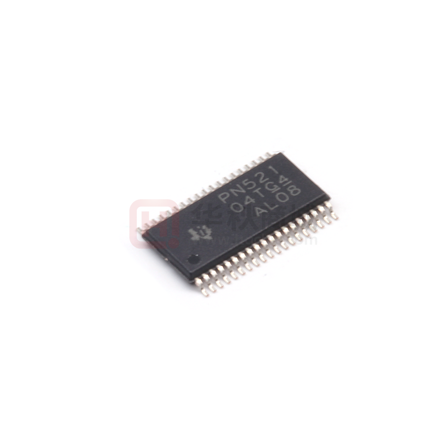
TPD12S521DBTR
ACTIVE
TSSOP
DBT
38
2000
RoHS & Green
NIPDAU
Level-2-260C-1 YEAR
-40 to 85
PN521
TPD12S521DBTRG4
ACTIVE
TSSOP
DBT
38
2000
RoHS & Green
NIPDAU
Level-2-260C-1 YEAR
-40 to 85
PN521
(1)
The marketing status values are defined as follows:
ACTIVE: Product device recommended for new designs.
LIFEBUY: TI has announced that the device will be discontinued, and a lifetime-buy period is in effect.
NRND: Not recommended for new designs. Device is in production to support existing customers, but TI does not recommend using this part in a new design.
PREVIEW: Device has been announced but is not in production. Samples may or may not be available.
OBSOLETE: TI has discontinued the production of the device.
(2)
RoHS: TI defines "RoHS" to mean semiconductor products that are compliant with the current EU RoHS requirements for all 10 RoHS substances, including the requirement that RoHS substance
do not exceed 0.1% by weight in homogeneous materials. Where designed to be soldered at high temperatures, "RoHS" products are suitable for use in specified lead-free processes. TI may
reference these types of products as "Pb-Free".
RoHS Exempt: TI defines "RoHS Exempt" to mean products that contain lead but are compliant with EU RoHS pursuant to a specific EU RoHS exemption.
Green: TI defines "Green" to mean the content of Chlorine (Cl) and Bromine (Br) based flame retardants meet JS709B low halogen requirements of


 工商网监
湘ICP备2023018690号
工商网监
湘ICP备2023018690号


