Product
Folder
Order
Now
Support &
Community
Tools &
Software
Technical
Documents
TPD4E001
SLLS682O – JULY 2006 – REVISED JULY 2019
TPD4E001 Low-Capacitance 4-Channel ESD-Protection for High-Speed Data Interfaces
1 Features
3 Description
•
The TPD4E001 is a four-channel Transient Voltage
Suppressor (TVS) based Electrostatic Discharge
(ESD) protection diode array. The TPD4E001 is rated
to dissipate ESD strikes at the maximum level
specified in the IEC 61000-4-2 international standard
(Level 4). This device has a 1.5-pF IO capacitance
per channel, making it ideal for use in high-speed
data IO interfaces. The ultra low leakage current (< 1
nA maximum) is suitable for precision analog
measurements in applications like glucose meters
and heart rate monitors.
1
•
•
•
•
•
•
•
IEC 61000-4-2 ESD Protection (Level 4)
– ±8-kV Contact Discharge
– ±15-kV Air-Gap Discharge
5.5-A Peak Pulse Current (8/20-µs Pulse)
IO Capacitance: 1.5 pF (Typical)
Low Leakage Current: 1 nA (Maximum)
Low Supply Current: 1 nA
0.9-V to 5.5-V Supply-Voltage Range
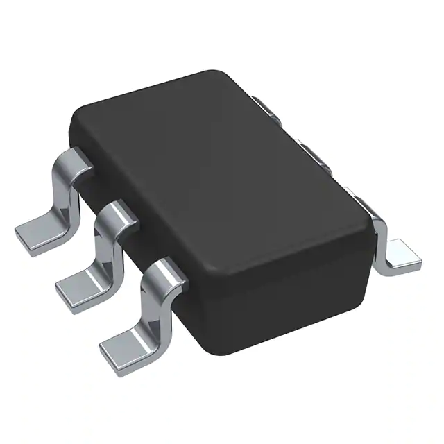
Space-Saving DRL, DBV, DCK, DPK, and DRS
Package Options
Alternate 2, 3, 6-Channel options Available:
TPD2E001, TPD3E001, TPD6E001
The TPD4E001 is available in DRL(SOT), DBV (SOT23), DCK (SC-70), DRS (QFN), and DPK (PUSON)
packages and is specified for –40°C to +85°C
operation. See also the TPD4E1U06DCKR and
TPD4E1U06DBVR which are p2p compatible with the
TPD4E001DCKR and TPD4E001DBVR. These
devices offer higher IEC protection, lower
capacitance, lower clamping voltage, and eliminate
the input capacitor requirement.
2 Applications
•
•
•
•
•
•
USB 2.0
Ethernet
FireWire™ Serial Bus
LVDS
SVGA Video Connections
Glucose Meters
Device Information(1)
PART NUMBER
PACKAGE
SOT (6)
TPD4E001
BODY SIZE (NOM)
1.60 mm × 1.20 mm
2.90 mm × 1.60 mm
SC70 (6)
2.00 mm × 1.25 mm
USON (6)
1.60 mm × 1.60 mm
SON (6)
3.00 mm × 3.00 mm
(1) For all available packages, see the orderable addendum at
the end of the data sheet.
Application Schematic
VBUS
0.1 µF
VCC
D+
D–
RT
GND
IO4
IO1
USB
Controller
D1
IO3
IO2
VBUS
D+
GND
D–
GND
1
An IMPORTANT NOTICE at the end of this data sheet addresses availability, warranty, changes, use in safety-critical applications,
intellectual property matters and other important disclaimers. PRODUCTION DATA.
�TPD4E001
SLLS682O – JULY 2006 – REVISED JULY 2019
www.ti.com
Table of Contents
1
2
3
4
5
6
7
Features ..................................................................
Applications ...........................................................
Description .............................................................
Revision History.....................................................
Pin Configuration and Functions .........................
Specifications.........................................................
1
1
1
2
4
5
6.1
6.2
6.3
6.4
6.5
6.6
6.7
5
5
5
5
6
6
7
Absolute Maximum Ratings .....................................
ESD Ratings—JEDEC Specification.........................
ESD Ratings—IEC Specification ..............................
Recommended Operating Conditions.......................
Thermal Information ..................................................
Electrical Characteristics...........................................
Typical Characteristics ..............................................
Detailed Description .............................................. 8
7.1 Overview ................................................................... 8
7.2 Functional Block Diagram ......................................... 8
7.3 Feature Description................................................... 8
7.4 Device Functional Modes.......................................... 8
8
Application and Implementation .......................... 9
8.1 Application Information.............................................. 9
8.2 Typical Application ................................................... 9
9 Power Supply Recommendations...................... 11
10 Layout................................................................... 11
10.1 Layout Guidelines ................................................. 11
10.2 Layout Example .................................................... 11
11 Device and Documentation Support ................. 12
11.1
11.2
11.3
11.4
11.5
11.6
11.7
Documentation Support ........................................
Related Links ........................................................
Receiving Notification of Documentation Updates
Community Resources..........................................
Trademarks ...........................................................
Electrostatic Discharge Caution ............................
Glossary ................................................................
12
12
12
12
12
12
12
12 Mechanical, Packaging, and Orderable
Information ........................................................... 12
4 Revision History
NOTE: Page numbers for previous revisions may differ from page numbers in the current version.
Changes from Revision N (March 2018) to Revision O
•
Added TPD4E001R DBV Package image and updated Pin Funtions table........................................................................... 4
Changes from Revision M (May 2017) to Revision N
•
Page
Page
TPD4E001DBVR Device Marking changed from NFY to NFYF ......................................................................................... 12
Changes from Revision L (May 2016) to Revision M
Page
•
Updated Pin Functions table and DCK2 Package image....................................................................................................... 4
•
Updated 'Surge Protection" to "IEC Specification" in ESD Ratings—IEC Specification table................................................ 5
Changes from Revision K (January 2015) to Revision L
Page
•
Added frequency test condition to Channel input capacitance in the Electrical Characteristics table ................................... 6
•
Added Community Resources ............................................................................................................................................. 12
Changes from Revision J (December 2013) to Revision K
•
Page
Added Pin Configuration and Functions section, ESD Ratings table, Feature Description section, Device Functional
Modes, Application and Implementation section, Power Supply Recommendations section, Layout section, Device
and Documentation Support section, and Mechanical, Packaging, and Orderable Information section .............................. 1
Changes from Revision I (September 2012) to Revision J
Page
•
Updated Description. .............................................................................................................................................................. 1
•
Removed Ordering Information table. .................................................................................................................................... 4
2
Submit Documentation Feedback
Copyright © 2006–2019, Texas Instruments Incorporated
Product Folder Links: TPD4E001
�TPD4E001
www.ti.com
SLLS682O – JULY 2006 – REVISED JULY 2019
Changes from Revision H (August 2012) to Revision I
Page
•
Added DCK2 package to Pin Out drawings. .......................................................................................................................... 4
•
Updated Electrical Characteristics table................................................................................................................................. 6
Changes from Revision G (December 2011) to Revision H
•
Page
Updated TOP-SIDE MARKING column in ORDERING INFORMATION table. ..................................................................... 4
Changes from Revision F (May 2011) to Revision G
Page
•
Updated document formatting. ............................................................................................................................................... 1
•
Added DPK (PUSON) package and package information. .................................................................................................... 4
Changes from Revision E (April 2011) to Revision F
•
Page
Added Peak Pulse Waveform Graph to Typical Operating Characteristics. .......................................................................... 7
Changes from Revision C (April 2007) to Revision D
•
Page
Added DBV (SOT-23) package and package information...................................................................................................... 4
Submit Documentation Feedback
Copyright © 2006–2019, Texas Instruments Incorporated
Product Folder Links: TPD4E001
3
�TPD4E001
SLLS682O – JULY 2006 – REVISED JULY 2019
www.ti.com
5 Pin Configuration and Functions
DRL Package
6-Pin SOT
Top View
DRS Package
6-Pin SON
Top View
IO1
1
6
VCC
IO2
2
5
IO4
GND
3
4
IO3
IO1
1
IO2
2
6
VCC
5
IO4
4
IO3
GND
GND
DCK2 Package
6-Pin SC70
Top View
IO1
1
6
VCC
IO2
2
5
IO4
GND
3
4
IO3
DPK Package
6-Pin USON
Top View
DBV or DCK Package
6-Pin SOT or SC70
Top View
IO1
1
6
IO4
GND
2
5
VCC
IO2
3
4
IO3
3
IO1
1
6
VCC
IO2
2
5
IO4
GND
3
4
IO3
TPD4E001R DBV Package
6-Pin SOT
Top View
IO1
1
6
IO3
VCC
2
5
GND
IO2
3
4
IO4
Pin Functions
PIN
NAME
GND
IOx
VCC
DRS, DRL, DPK
DBV, DCK
TPD4E001R
3
2
5
1
1
1
2
3
3
4
4
4
5
6
6
6
5
2
Exposed thermal
pad (DRS package only)
4
I/O
—
DESCRIPTION
Ground
I
ESD-protected channel
I
Power-supply input. Bypass VCC to GND with a 0.1-μF
ceramic capacitor
—
Exposed thermal pad. Connect to GND or leave floating
Submit Documentation Feedback
Copyright © 2006–2019, Texas Instruments Incorporated
Product Folder Links: TPD4E001
�TPD4E001
www.ti.com
SLLS682O – JULY 2006 – REVISED JULY 2019
6 Specifications
6.1 Absolute Maximum Ratings
over operating free-air temperature range (unless otherwise noted) (1)
VCC
MIN
MAX
UNIT
–0.3
7
V
–0.3
VCC + 0.3
V
VI/O
IO voltage tolerance
I(Surge)
IEC 61000-4-5 peak pulse current (TP = 8/20 µs), IOx pins
5.5
A
P(Surge)
IEC 61000-4-5 peak pulse power (TP = 8/20 µs), IOx pins
100
W
TJ
Junction temperature
150
°C
Bump temperature (soldering)
Infrared (15 s)
220
Vapor phase (60 s)
215
Lead temperature (soldering, 10 s)
Tstg
(1)
Storage temperature
–65
°C
300
°C
150
°C
Stresses beyond those listed under Absolute Maximum Ratings may cause permanent damage to the device. These are stress ratings
only, which do not imply functional operation of the device at these or any other conditions beyond those indicated under Recommended
Operating Conditions. Exposure to absolute-maximum-rated conditions for extended periods may affect device reliability.
6.2 ESD Ratings—JEDEC Specification
VALUE
UNIT
TPD4E001 in DRS, DRL, and DPK Packages
Human-body model (HBM), per
ANSI/ESDA/JEDEC JS-001 (1)
V(ESD)
Electrostatic discharge
Charged-device model (CDM), per JEDEC
specification JESD22-C101 (2)
All pins except 1, 2, 4, and
5
±2000
Pins 1, 2, 4, and 5
±15000
All pins
±1000
All pins except 1, 3, 4, and
6
±2000
Pins 1, 3, 4, and 6
±15000
All pins
±1000
V
TPD4E001 in DBV and DCK Packages
V(ESD)
Electrostatic discharge
Human-body model (HBM), per
ANSI/ESDA/JEDEC JS-001 (1)
Charged-device model (CDM), per JEDEC
specification JESD22-C101 (2)
(1)
(2)
V
JEDEC document JEP155 states that 500-V HBM allows safe manufacturing with a standard ESD control process.
JEDEC document JEP157 states that 250-V CDM allows safe manufacturing with a standard ESD control process.
6.3 ESD Ratings—IEC Specification
VALUE
UNIT
TPD4E001 in DRS, DRL, and DPK Packages
V(ESD)
Electrostatic discharge
IEC 61000-4-2 contact discharge
All pins
±8000
IEC 61000-4-2 air-gap discharge
All pins
±15000
V
TPD4E001 in DBV and DCK Packages
V(ESD)
Electrostatic discharge
IEC 61000-4-2 contact discharge
All pins
±8000
IEC 61000-4-2 air-gap discharge
All pins
±15000
V
6.4 Recommended Operating Conditions
over operating free-air temperature range (unless otherwise noted)
TA
Operating free-air temperature
Operating voltage
VCC pin
IO1, IO2 pins
MIN
MAX
–40
85
0.9
5.5
0
VCC
Submit Documentation Feedback
Copyright © 2006–2019, Texas Instruments Incorporated
Product Folder Links: TPD4E001
UNIT
°C
V
5
�TPD4E001
SLLS682O – JULY 2006 – REVISED JULY 2019
www.ti.com
6.5 Thermal Information
TPD4E001
THERMAL METRIC
(1)
DRL
(SOT)
DBV
(SOT)
DCK
(SC70)
DPK
(USON)
DRS (SON)
6 PINS
6 PINS
6 PINS
6 PINS
6 PINS
UNIT
RθJA
Junction-to-ambient thermal resistance
226.4
259.7
251.1
247.6
91.9
°C/W
RθJC(top)
Junction-to-case (top) thermal resistance
90.3
186.5
88.1
124.8
106.9
°C/W
RθJB
Junction-to-board thermal resistance
61.2
107.6
54.8
204.2
64.8
°C/W
ψJT
Junction-to-top characterization parameter
6.7
71.4
1.7
19.2
10.2
°C/W
ψJB
Junction-to-board characterization parameter
61
107.1
54.1
209.3
64.9
°C/W
RθJC(bot)
Junction-to-case (bottom) thermal resistance
N/A
N/A
N/A
N/A
29.9
°C/W
(1)
For more information about traditional and new thermal metrics, see the Semiconductor and IC Package Thermal Metrics application
report.
6.6 Electrical Characteristics
over operating free-air temperature range (unless otherwise noted), VCC = 5 V ± 10%
PARAMETER
TEST CONDITIONS
VCC
Supply voltage
ICC
Supply current
VF
Diode forward voltage
IF = 10 mA
VBR
Breakdown Voltage
IBR = 10 mA
VC
Channel clamp voltage
MIN
TYP (1)
MAX
5.5
V
1
100
nA
0.95
V
0.9
0.65
11
TA = 25°C, ±15-kV HBM,
IF = 10 A
Positive transients
TA = 25°C,
±8-kV contact discharge
(IEC 61000-4-2), IF = 24 A
Positive transients
TA = 25°C,
±15-kV air-gap discharge
(IEC 61000-4-2), IF = 45 A
Positive transients
Surge strike on IO pin,
GND pin grounded,
IPP = 5 A, 8/20 µs (2)
V
VCC + 25
Negative transients
–25
VCC + 60
Negative transients
–60
VCC + 100
Negative transients
Positive transients
UNIT
V
–100
17
VRWM
Reverse stand-off voltage
IO pin to GND pin
5.5
V
II/O
Channel leakage current
Vi/o = GND to VCC
±1
nA
CI/O
Channel input capacitance
VCC = 5 V, bias of VCC/2; ƒ = 10 MHz
(1)
(2)
6
1.5
pF
Typical values are at VCC = 5 V and TA = 25°C.
Non-repetitive current pulse 8/20 µs exponentially decaying waveform according to ICE61000-4-5.
Submit Documentation Feedback
Copyright © 2006–2019, Texas Instruments Incorporated
Product Folder Links: TPD4E001
�TPD4E001
www.ti.com
SLLS682O – JULY 2006 – REVISED JULY 2019
6.7 Typical Characteristics
1000
2.20
IO Leakage Current (pA)
1.80
1.60
1.40
1.20
100
10
1.00
1
0.00
1.00
2.00
2.50
3.00
4.00
5.00
–40
25
IO Voltage (V)
IPK (A)
Figure 1. IO Capacitance vs IO Voltage (VCC = 5 V)
6.0
5.5
5.0
4.5
4.0
3.5
3.0
2.5
2.0
1.5
1.0
0.5
0.0
45
65
85
Temperature (°C)
Figure 2. IO Leakage Current vs Temperature (VCC = 5.5 V)
100
90
80
70
Current (A)
60
50
40
PPK (W)
IO Capacitance (pF)
2.00
30
Power (W)
20
10
0
5
10
15
20
25
30
Time (μs)
35
40
45
0
50
Figure 3. Peak Pulse Waveform, VCC = 5.5 V
Submit Documentation Feedback
Copyright © 2006–2019, Texas Instruments Incorporated
Product Folder Links: TPD4E001
7
�TPD4E001
SLLS682O – JULY 2006 – REVISED JULY 2019
www.ti.com
7 Detailed Description
7.1 Overview
The TPD4E001 is a four-channel transient voltage suppressor (TVS) based ESD protection diode array. The
TPD4E001 is rated to dissipate ESD strikes at the maximum level specified in the IEC 61000-4-2 international
standard (Level 4). This device has a 1.5-pF IO capacitance per channel, making it ideal for use in high-speed
data IO interfaces. The ultra-low leakage current (