Sample &
Buy
Product
Folder
Support &
Community
Tools &
Software
Technical
Documents
TPD4E004
SLVS729B – FEBRUARY 2008 – REVISED MARCH 2016 2016
TPD4E004 4-Channel ESD-Protection Array For High-Speed Data Interfaces
1 Features
3 Description
•
The TPD4E004 is a low-capacitance transient voltage
suppression (TVS) device. TPD4E004 is designed to
protect
sensitive
electronics
attached
to
communication lines from electrostatic discharge
(ESD). Each of the four channels consists of a pair of
diodes that steer ESD current pulses to VCC or GND.
The TPD4E004 protects against ESD pulses up to
±15-kV Human-Body Model (HBM) and, as specified
in IEC 61000-4-2, ±8-kV contact discharge and ±12kV air-gap Discharge. This device has 1.6-pF of
capacitance per channel, making it ideal for use in
high-speed data IO interfaces.
1
•
•
•
•
•
IEC 61000-4-2 ESD Protection
– ±8-kV IEC 61000-4-2 Contact Discharge
– ±12-kV IEC 61000-4-2 Air-Gap Discharge
ANSI/ESDA/JEDEC JS-001
– ±15-kV Human Body Model (HBM)
Low 1.6-pF Input Capacitance
0.9-V to 5.5-V Supply Voltage Range
4-Channel Device
Space-Saving SON (DRY) Package
The TPD4E004 is a quad-ESD structure designed for
USB, ethernet, and other high-speed applications.
2 Applications
•
•
•
•
•
•
•
USB
Ethernet
FireWire
Videos
Cell Phones
SVGA Video Connections
Glucose Meters
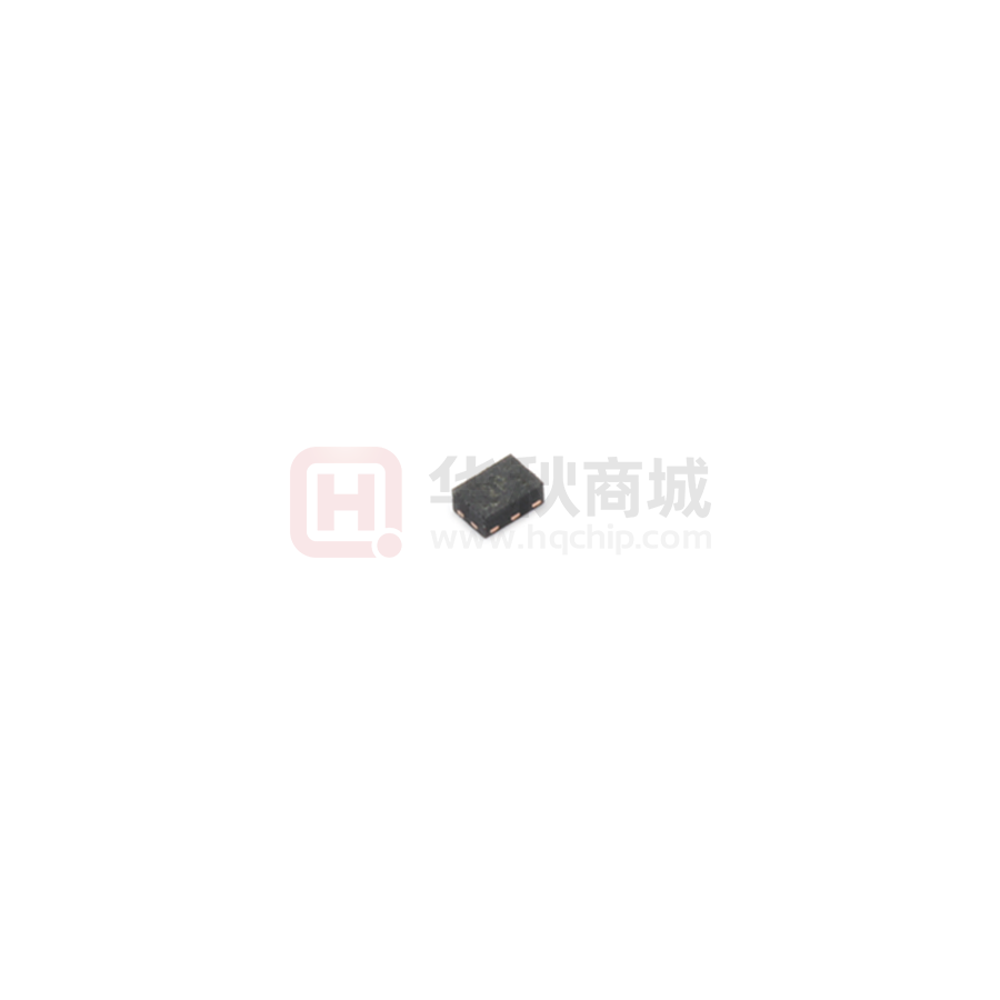
Device Information(1)
PART NUMBER
TPD4E004
PACKAGE
SON (6)
BODY SIZE (NOM)
1.45 mm × 1.00 mm
(1) For all available packages, see the orderable addendum at
the end of the data sheet.
Application Schematic
VBUS
0.1 µF
VCC
D+
D–
RT
GND
IO4
IO1
USB
Controller
D1
IO3
IO2
VBUS
D+
GND
D–
GND
1
An IMPORTANT NOTICE at the end of this data sheet addresses availability, warranty, changes, use in safety-critical applications,
intellectual property matters and other important disclaimers. PRODUCTION DATA.
�TPD4E004
SLVS729B – FEBRUARY 2008 – REVISED MARCH 2016 2016
www.ti.com
Table of Contents
1
2
3
4
5
6
7
Features ..................................................................
Applications ...........................................................
Description .............................................................
Revision History.....................................................
Pin Configuration and Functions .........................
Specifications.........................................................
1
1
1
2
3
4
6.1
6.2
6.3
6.4
6.5
6.6
4
4
4
4
5
6
Absolute Maximum Ratings ......................................
ESD Ratings..............................................................
Recommended Operating Conditions.......................
Thermal Information ..................................................
Electrical Characteristics...........................................
Typical Characteristics ..............................................
Detailed Description .............................................. 7
7.1 Overview ................................................................... 7
7.2 Functional Block Diagram ......................................... 7
7.3 Feature Description................................................... 7
7.4 Device Functional Modes.......................................... 7
8
Application and Implementation .......................... 8
8.1 Application Information.............................................. 8
8.2 Typical Application ................................................... 8
9 Power Supply Recommendations........................ 9
10 Layout................................................................... 10
10.1 Layout Guidelines ................................................. 10
10.2 Layout Example .................................................... 10
11 Device and Documentation Support ................. 11
11.1
11.2
11.3
11.4
11.5
Documentation Support ........................................
Community Resources..........................................
Trademarks ...........................................................
Electrostatic Discharge Caution ............................
Glossary ................................................................
11
11
11
11
11
12 Mechanical, Packaging, and Orderable
Information ........................................................... 11
4 Revision History
NOTE: Page numbers for previous revisions may differ from page numbers in the current version.
Changes from Revision A (February 2008) to Revision B
Page
•
Added Device Information table, ESD Ratings table, Feature Description section, Device Functional Modes,
Application and Implementation section, Power Supply Recommendations section, Layout section, Device and
Documentation Support section, and Mechanical, Packaging, and Orderable Information section. .................................... 1
•
Deleted the ordering information ........................................................................................................................................... 1
2
Submit Documentation Feedback
Copyright © 2008–2016, Texas Instruments Incorporated
Product Folder Links: TPD4E004
�TPD4E004
www.ti.com
SLVS729B – FEBRUARY 2008 – REVISED MARCH 2016 2016
5 Pin Configuration and Functions
DRY Package
6-Pin SON
Top View
IO1
1
6
VCC
IO2
2
5
IO4
GND
3
4
IO3
Pin Functions
PIN
NO.
NAME
I/O
DESCRIPTION
1
IO1
IO
ESD-protected channel
2
IO2
IO
ESD-protected channel
3
GND
GND
4
IO3
IO
ESD-protected channel
5
IO4
IO
ESD-protected channel
6
VCC
PWR
Ground
Power-supply input
Submit Documentation Feedback
Copyright © 2008–2016, Texas Instruments Incorporated
Product Folder Links: TPD4E004
3
�TPD4E004
SLVS729B – FEBRUARY 2008 – REVISED MARCH 2016 2016
www.ti.com
6 Specifications
6.1 Absolute Maximum Ratings
over operating free-air temperature range (unless otherwise noted)
VCC
Supply voltage
VIO
Input/output voltage
Bump temperature (soldering)
(1)
MIN
MAX
UNIT
–0.3
5.5
V
–0.3
VCC + 0.3
V
Infrared (15 s)
220
Vapor phase (60 s)
215
°C
Lead temperature (soldering, 10 s)
300
°C
TJ
Junction temperature
150
°C
Tstg
Storage temperature
150
°C
(1)
–65
Stresses beyond those listed under Absolute Maximum Ratings may cause permanent damage to the device. These are stress ratings
only, which do not imply functional operation of the device at these or any other conditions beyond those indicated under Recommended
Operating Conditions. Exposure to absolute-maximum-rated conditions for extended periods may affect device reliability.
6.2 ESD Ratings
VALUE
Human-body model (HBM), per ANSI/ESDA/JEDEC JS-001
Electrostatic
discharge
V(ESD)
IEC 61000-4-2
UNIT
±15000
Contact Discharge
±8000
Air-Gap Discharge
±12000
V
6.3 Recommended Operating Conditions
over operating free-air temperature range (unless otherwise noted)
MIN
MAX
UNIT
TA
Operating free-air temperature
–40
85
°C
VCC
Operating voltage for pin VCC
0.9
5.5
V
0
Minimum of:
(5.8, VCC)
V
VIO
Operating voltage for pins IO1, IO2, IO3, and IO4
6.4 Thermal Information
TPD4E004
THERMAL METRIC (1)
DRY (SON)
UNIT
6 PINS
RθJA
Junction-to-ambient thermal resistance
414.8
°C/W
RθJC(top)
Junction-to-case (top) thermal resistance
258.6
°C/W
RθJB
Junction-to-board thermal resistance
251.6
°C/W
ψJT
Junction-to-top characterization parameter
70.6
°C/W
ψJB
Junction-to-board characterization parameter
248.2
°C/W
RθJC(bot)
Junction-to-case (bottom) thermal resistance
n/a
°C/W
(1)
4
For more information about traditional and new thermal metrics, see the Semiconductor and IC Package Thermal Metrics application
report, SPRA953.
Submit Documentation Feedback
Copyright © 2008–2016, Texas Instruments Incorporated
Product Folder Links: TPD4E004
�TPD4E004
www.ti.com
SLVS729B – FEBRUARY 2008 – REVISED MARCH 2016 2016
6.5 Electrical Characteristics
VCC = 0.9 V to 5.5 V, TA = TMIN to TMAX (unless otherwise noted)
PARAMETER
TEST CONDITIONS
VCC
Supply voltage
ICC
Supply current
VF
Diode forward voltage
II
Channel leakage current
VBR
Break-down voltage
II = 10 μA
CI/O
Channel input capacitance
VCC = 5 V, Bias of VCC/2, f = 10 MHz
(1)
MIN
TYP (1)
0.9
IF = 1 mA
MAX
UNIT
5.5
V
500
nA
0.8
V
±1
nA
6
1.6
8
V
2
pF
Typical values are at VCC = 5 V and TA = 25°C.
Submit Documentation Feedback
Copyright © 2008–2016, Texas Instruments Incorporated
Product Folder Links: TPD4E004
5
�TPD4E004
SLVS729B – FEBRUARY 2008 – REVISED MARCH 2016 2016
www.ti.com
6.6 Typical Characteristics
160
70
140
60
120
100
Leakage Current (pA)
IO Current (mA)
50
80
60
40
20
40
30
20
10
0
0
1.05
1.15
1.25
1.35
1.45
1.55
–40
55
25
IO Voltage (V)
85
Temperature (°C)
Figure 1. Forward Diode Voltage (Upper Clamp Diode)
(VCC = 0 V, DC Sweep Across the IO Pin)
Figure 2. Leakage Current vs Temperature (VIO = 2.5 V)
5.0
16.0
14.0
4.0
IO Capacitance (pF)
12.0
IO Current (µA)
10.0
8.0
6.0
4.0
3.0
2.0
1.0
2.0
0.0
0.0
0.0
1.0
2.0
3.0
4.0
5.0
6.0
7.0
1
3
4
5
IO Voltage (V)
IO Voltage (V)
Figure 3. Reverse Diode Curve Current IO to Gnd
(VCC = Open)
6
2
Figure 4. IO Capacitance vs Input Voltage
(VCC = 5 V)
Submit Documentation Feedback
Copyright © 2008–2016, Texas Instruments Incorporated
Product Folder Links: TPD4E004
�TPD4E004
www.ti.com
SLVS729B – FEBRUARY 2008 – REVISED MARCH 2016 2016
7 Detailed Description
7.1 Overview
The TPD4E004 is a four-channel TVS protection diode array. The TPD4E004 is rated to dissipate contact ESD
strikes of ±8-kV contact and ±12-kV air-gap, meeting Level 4 as specified in the IEC 61000-4-2 international
standard. This device has a 1.6-pF IO capacitance per channel, making it ideal for use in high-speed data IO
interfaces.
7.2 Functional Block Diagram
VCC
IO1
IO3
IO2
IO4
GND
7.3 Feature Description
TPD4E004 is a TVS which provides ESD protection for up to four channels, withstanding up to ±8-kV contact
and ±12-kV air-gap ESD per IEC 61000-4-2. The monolithic technology yields exceptionally small variations in
capacitance between any IO pin of TPD4E004. The small footprint is ideal for applications where space-saving
designs are important.
7.4 Device Functional Modes
The TPD4E004 device is a passive integrated circuit that triggers when voltages are above VBR or below the
diodes VF of approximately –0.3 V. During ESD events, voltages as high as ±8-kV contact and ±12-kV air-gap
ESD can be directed to ground via the internal diodes. Once the voltages on the protected line fall below the
trigger levels of TPD4E004 (usually within 10’s of nano-seconds) the device reverts back to its high-impedance
state.
Submit Documentation Feedback
Copyright © 2008–2016, Texas Instruments Incorporated
Product Folder Links: TPD4E004
7
�TPD4E004
SLVS729B – FEBRUARY 2008 – REVISED MARCH 2016 2016
www.ti.com
8 Application and Implementation
NOTE
Information in the following applications sections is not part of the TI component
specification, and TI does not warrant its accuracy or completeness. TI’s customers are
responsible for determining suitability of components for their purposes. Customers should
validate and test their design implementation to confirm system functionality.
8.1 Application Information
TPD4E004 is a diode array type TVS which is typically used to provide a path to ground for dissipating ESD
events on hi-speed signal lines between a human interface connector and a system. As the current from ESD
passes through the TVS, only a small voltage drop is present across the diode. This is the voltage presented to
the protected IC. The low RDYN of the triggered TVS holds this voltage, VCLAMP, to a tolerable level for the
protected IC.
8.2 Typical Application
VBUS
0.1 µF
VCC
D+
D–
RT
GND
IO4
IO1
USB
Controller
IO3
IO2
VBUS
D+
GND
D–
GND
Figure 5. Application Schematic
8.2.1 Design Requirements
For this design example, a single TPD4E004 is used to protect all the pins of two USB2.0 connectors. Table 1
lists the design parameters for the USB application.
Table 1. Design Parameters
DESIGN PARAMETER
VALUE
Signal range on IO1, IO2, IO3, and IO4
0 V to 3.6 V
Signal voltage range on VCC
0 V to 5.5 V
Operating Frequency
240 MHz
8.2.2 Detailed Design Procedure
When placed near the USB connectors, the TPD4E004 ESD solution offers little or no signal distortion during
normal operation due to low IO capacitance and ultra-low leakage current specifications. The TPD4E004 ensures
that the core circuitry is protected and the system is functioning properly in the event of an ESD strike. For
proper operation, see the the following layout and design guidelines should be followed:
1. Place the TPD4E004 solution close to the connectors. This allows the TPD4E004 to take away the energy
8
Submit Documentation Feedback
Copyright © 2008–2016, Texas Instruments Incorporated
Product Folder Links: TPD4E004
�TPD4E004
www.ti.com
2.
3.
4.
5.
SLVS729B – FEBRUARY 2008 – REVISED MARCH 2016 2016
associated with ESD strike before it reaches the internal circuitry of the system board.
Place a 0.1-μF capacitor very close to the VCC pin. This limits any momentary voltage surge at the IO pin
during the ESD strike event.
Ensure that there is enough metallization for the VCC and GND loop. During normal operation, the TPD4E004
consumes nA leakage current. But during the ESD event, VCC and GND may see 15-A to 30-A of current,
depending on the ESD level. Sufficient current path enables safe discharge of all the energy associated with
the ESD strike.
Leave the unused IO pins floating. In this example of protecting two USB ports, none of the IO pins will be
left unused.
The VCC pin can be connected in two different ways:
(a) If the VCC pin is connected to the system power supply, the TPD4E004 works as a transient suppressor
for any signal swing above VCC + VF. A 0.1-μF capacitor on the device VCC pin is recommended for ESD
bypass.
(b) If the VCC pin is not connected to the system power supply, the TPD4E004 can tolerate higher signal
swing in the range up to 5.8 V. Please note that a 0.1-μF capacitor is still recommended at the VCC pin
for ESD bypass.
8.2.3 Application Curves
Figure 6 is a capture of the voltage clamping waveform of TPD4E004 during an +8kV Contact IEC 61000-4-2
ESD strike.
120
100
Amplitude (V)
80
60
40
20
0
–20
0
5
10
15
20
25
30
35
40
45
50
Time (ns)
Figure 6. IEC ESD Clamping Waveforms +8-KV Contact
9 Power Supply Recommendations
This device is a passive ESD protection device so there is no need to power it. Make sure that the maximum
voltage specifications for each pin are not violated.
Submit Documentation Feedback
Copyright © 2008–2016, Texas Instruments Incorporated
Product Folder Links: TPD4E004
9
�TPD4E004
SLVS729B – FEBRUARY 2008 – REVISED MARCH 2016 2016
www.ti.com
10 Layout
10.1 Layout Guidelines
•
•
•
The optimum placement is as close to the connector as possible.
– EMI during an ESD event can couple from the trace being struck to other nearby unprotected traces,
resulting in early system failures.
– The PCB designer needs to minimize the possibility of EMI coupling by keeping any unprotected traces
away from the protected traces which are between the TVS and the connector.
Route the protected traces as straight as possible.
Eliminate any sharp corners on the protected traces between the TVS and the connector by using rounded
corners with the largest radii possible.
– Electric fields tend to build up on corners, increasing EMI coupling.
10.2 Layout Example
D1
TPD4E004
1
D1
D2
D2
Legend
VIA to Internal GND Plane
VIA to Internal VBUS Plane
Pin to GND
Signal VIA in SMD Pad
Layer 1 Routing
Layer 2 Routing
Figure 7. TPD4E004 Layout Example
10
Submit Documentation Feedback
Copyright © 2008–2016, Texas Instruments Incorporated
Product Folder Links: TPD4E004
�TPD4E004
www.ti.com
SLVS729B – FEBRUARY 2008 – REVISED MARCH 2016 2016
11 Device and Documentation Support
11.1 Documentation Support
11.1.1 Related Documentation
For related documentation see the following:
•
•
Reading and Understanding an ESD Protection Datasheet, SLLA305
ESD Protection Layout Guide, SLVA680
11.2 Community Resources
The following links connect to TI community resources. Linked contents are provided "AS IS" by the respective
contributors. They do not constitute TI specifications and do not necessarily reflect TI's views; see TI's Terms of
Use.
TI E2E™ Online Community TI's Engineer-to-Engineer (E2E) Community. Created to foster collaboration
among engineers. At e2e.ti.com, you can ask questions, share knowledge, explore ideas and help
solve problems with fellow engineers.
Design Support TI's Design Support Quickly find helpful E2E forums along with design support tools and
contact information for technical support.
11.3 Trademarks
E2E is a trademark of Texas Instruments.
All other trademarks are the property of their respective owners.
11.4 Electrostatic Discharge Caution
These devices have limited built-in ESD protection. The leads should be shorted together or the device placed in conductive foam
during storage or handling to prevent electrostatic damage to the MOS gates.
11.5 Glossary
SLYZ022 — TI Glossary.
This glossary lists and explains terms, acronyms, and definitions.
12 Mechanical, Packaging, and Orderable Information
The following pages include mechanical, packaging, and orderable information. This information is the most
current data available for the designated devices. This data is subject to change without notice and revision of
this document. For browser-based versions of this data sheet, refer to the left-hand navigation.
Submit Documentation Feedback
Copyright © 2008–2016, Texas Instruments Incorporated
Product Folder Links: TPD4E004
11
�PACKAGE OPTION ADDENDUM
www.ti.com
22-Jan-2016
PACKAGING INFORMATION
Orderable Device
Status
(1)
Package Type Package Pins Package
Drawing
Qty
Eco Plan
Lead/Ball Finish
MSL Peak Temp
(2)
(6)
(3)
Op Temp (°C)
Device Marking
(4/5)
TPD4E004DRYR
ACTIVE
SON
DRY
6
5000
Green (RoHS
& no Sb/Br)
CU NIPDAU
Level-1-260C-UNLIM
-40 to 85
2P
TPD4E004DRYRG4
ACTIVE
SON
DRY
6
5000
Green (RoHS
& no Sb/Br)
CU NIPDAU
Level-1-260C-UNLIM
-40 to 85
2P
(1)
The marketing status values are defined as follows:
ACTIVE: Product device recommended for new designs.
LIFEBUY: TI has announced that the device will be discontinued, and a lifetime-buy period is in effect.
NRND: Not recommended for new designs. Device is in production to support existing customers, but TI does not recommend using this part in a new design.
PREVIEW: Device has been announced but is not in production. Samples may or may not be available.
OBSOLETE: TI has discontinued the production of the device.
(2)
Eco Plan - The planned eco-friendly classification: Pb-Free (RoHS), Pb-Free (RoHS Exempt), or Green (RoHS & no Sb/Br) - please check http://www.ti.com/productcontent for the latest availability
information and additional product content details.
TBD: The Pb-Free/Green conversion plan has not been defined.
Pb-Free (RoHS): TI's terms "Lead-Free" or "Pb-Free" mean semiconductor products that are compatible with the current RoHS requirements for all 6 substances, including the requirement that
lead not exceed 0.1% by weight in homogeneous materials. Where designed to be soldered at high temperatures, TI Pb-Free products are suitable for use in specified lead-free processes.
Pb-Free (RoHS Exempt): This component has a RoHS exemption for either 1) lead-based flip-chip solder bumps used between the die and package, or 2) lead-based die adhesive used between
the die and leadframe. The component is otherwise considered Pb-Free (RoHS compatible) as defined above.
Green (RoHS & no Sb/Br): TI defines "Green" to mean Pb-Free (RoHS compatible), and free of Bromine (Br) and Antimony (Sb) based flame retardants (Br or Sb do not exceed 0.1% by weight
in homogeneous material)
(3)
MSL, Peak Temp. - The Moisture Sensitivity Level rating according to the JEDEC industry standard classifications, and peak solder temperature.
(4)
There may be additional marking, which relates to the logo, the lot trace code information, or the environmental category on the device.
(5)
Multiple Device Markings will be inside parentheses. Only one Device Marking contained in parentheses and separated by a "~" will appear on a device. If a line is indented then it is a continuation
of the previous line and the two combined represent the entire Device Marking for that device.
(6)
Lead/Ball Finish - Orderable Devices may have multiple material finish options. Finish options are separated by a vertical ruled line. Lead/Ball Finish values may wrap to two lines if the finish
value exceeds the maximum column width.
Important Information and Disclaimer:The information provided on this page represents TI's knowledge and belief as of the date that it is provided. TI bases its knowledge and belief on information
provided by third parties, and makes no representation or warranty as to the accuracy of such information. Efforts are underway to better integrate information from third parties. TI has taken and
continues to take reasonable steps to provide representative and accurate information but may not have conducted destructive testing or chemical analysis on incoming materials and chemicals.
TI and TI suppliers consider certain information to be proprietary, and thus CAS numbers and other limited information may not be available for release.
Addendum-Page 1
Samples
�PACKAGE OPTION ADDENDUM
www.ti.com
22-Jan-2016
In no event shall TI's liability arising out of such information exceed the total purchase price of the TI part(s) at issue in this document sold by TI to Customer on an annual basis.
Addendum-Page 2
�PACKAGE MATERIALS INFORMATION
www.ti.com
29-Aug-2017
TAPE AND REEL INFORMATION
*All dimensions are nominal
Device
Package Package Pins
Type Drawing
SPQ
Reel
Reel
A0
Diameter Width (mm)
(mm) W1 (mm)
B0
(mm)
K0
(mm)
P1
(mm)
W
Pin1
(mm) Quadrant
TPD4E004DRYR
SON
DRY
6
5000
179.0
8.4
1.2
1.65
0.7
4.0
8.0
Q1
TPD4E004DRYR
SON
DRY
6
5000
180.0
9.5
1.2
1.65
0.7
4.0
8.0
Q1
Pack Materials-Page 1
�PACKAGE MATERIALS INFORMATION
www.ti.com
29-Aug-2017
*All dimensions are nominal
Device
Package Type
Package Drawing
Pins
SPQ
Length (mm)
Width (mm)
Height (mm)
TPD4E004DRYR
SON
DRY
6
5000
203.0
203.0
35.0
TPD4E004DRYR
SON
DRY
6
5000
189.0
185.0
36.0
Pack Materials-Page 2
�GENERIC PACKAGE VIEW
DRY 6
USON - 0.6 mm max height
PLASTIC SMALL OUTLINE - NO LEAD
Images above are just a representation of the package family, actual package may vary.
Refer to the product data sheet for package details.
4207181/G
�PACKAGE OUTLINE
DRY0006A
USON - 0.6 mm max height
SCALE 8.500
PLASTIC SMALL OUTLINE - NO LEAD
1.05
0.95
B
A
PIN 1 INDEX AREA
1.5
1.4
C
0.6 MAX
SEATING PLANE
0.05
0.00
0.08 C
3X 0.6
SYMM
(0.127) TYP
(0.05) TYP
3
4
4X
0.5
SYMM
2X
1
1
6
6X
0.4
0.3
PIN 1 ID
(OPTIONAL)
5X
0.25
0.15
0.1
0.05
0.35
0.25
C A B
C
4222894/A 01/2018
NOTES:
1. All linear dimensions are in millimeters. Any dimensions in parenthesis are for reference only. Dimensioning and tolerancing
per ASME Y14.5M.
2. This drawing is subject to change without notice.
www.ti.com
�EXAMPLE BOARD LAYOUT
DRY0006A
USON - 0.6 mm max height
PLASTIC SMALL OUTLINE - NO LEAD
SYMM
(0.35)
5X (0.3)
6
1
6X (0.2)
SYMM
4X (0.5)
4
3
(R0.05) TYP
(0.6)
LAND PATTERN EXAMPLE
1:1 RATIO WITH PKG SOLDER PADS
EXPOSED METAL SHOWN
SCALE:40X
0.05 MAX
ALL AROUND
EXPOSED
METAL
0.05 MIN
ALL AROUND
EXPOSED
METAL
METAL
SOLDER MASK
OPENING
NON SOLDER MASK
DEFINED
METAL UNDER
SOLDER MASK
SOLDER MASK
OPENING
SOLDER MASK
DEFINED
(PREFERRED)
SOLDER MASK DETAILS
4222894/A 01/2018
NOTES: (continued)
3. For more information, see QFN/SON PCB application report in literature No. SLUA271 (www.ti.com/lit/slua271).
www.ti.com
�EXAMPLE STENCIL DESIGN
DRY0006A
USON - 0.6 mm max height
PLASTIC SMALL OUTLINE - NO LEAD
SYMM
(0.35)
5X (0.3)
1
6
6X (0.2)
SYMM
4X (0.5)
4
3
(R0.05) TYP
(0.6)
SOLDER PASTE EXAMPLE
BASED ON 0.075 - 0.1 mm THICK STENCIL
SCALE:40X
4222894/A 01/2018
NOTES: (continued)
4. Laser cutting apertures with trapezoidal walls and rounded corners may offer better paste release. IPC-7525 may have alternate
design recommendations.
www.ti.com
�IMPORTANT NOTICE
Texas Instruments Incorporated (TI) reserves the right to make corrections, enhancements, improvements and other changes to its
semiconductor products and services per JESD46, latest issue, and to discontinue any product or service per JESD48, latest issue. Buyers
should obtain the latest relevant information before placing orders and should verify that such information is current and complete.
TI’s published terms of sale for semiconductor products (http://www.ti.com/sc/docs/stdterms.htm) apply to the sale of packaged integrated
circuit products that TI has qualified and released to market. Additional terms may apply to the use or sale of other types of TI products and
services.
Reproduction of significant portions of TI information in TI data sheets is permissible only if reproduction is without alteration and is
accompanied by all associated warranties, conditions, limitations, and notices. TI is not responsible or liable for such reproduced
documentation. Information of third parties may be subject to additional restrictions. Resale of TI products or services with statements
different from or beyond the parameters stated by TI for that product or service voids all express and any implied warranties for the
associated TI product or service and is an unfair and deceptive business practice. TI is not responsible or liable for any such statements.
Buyers and others who are developing systems that incorporate TI products (collectively, “Designers”) understand and agree that Designers
remain responsible for using their independent analysis, evaluation and judgment in designing their applications and that Designers have
full and exclusive responsibility to assure the safety of Designers' applications and compliance of their applications (and of all TI products
used in or for Designers’ applications) with all applicable regulations, laws and other applicable requirements. Designer represents that, with
respect to their applications, Designer has all the necessary expertise to create and implement safeguards that (1) anticipate dangerous
consequences of failures, (2) monitor failures and their consequences, and (3) lessen the likelihood of failures that might cause harm and
take appropriate actions. Designer agrees that prior to using or distributing any applications that include TI products, Designer will
thoroughly test such applications and the functionality of such TI products as used in such applications.
TI’s provision of technical, application or other design advice, quality characterization, reliability data or other services or information,
including, but not limited to, reference designs and materials relating to evaluation modules, (collectively, “TI Resources”) are intended to
assist designers who are developing applications that incorporate TI products; by downloading, accessing or using TI Resources in any
way, Designer (individually or, if Designer is acting on behalf of a company, Designer’s company) agrees to use any particular TI Resource
solely for this purpose and subject to the terms of this Notice.
TI’s provision of TI Resources does not expand or otherwise alter TI’s applicable published warranties or warranty disclaimers for TI
products, and no additional obligations or liabilities arise from TI providing such TI Resources. TI reserves the right to make corrections,
enhancements, improvements and other changes to its TI Resources. TI has not conducted any testing other than that specifically
described in the published documentation for a particular TI Resource.
Designer is authorized to use, copy and modify any individual TI Resource only in connection with the development of applications that
include the TI product(s) identified in such TI Resource. NO OTHER LICENSE, EXPRESS OR IMPLIED, BY ESTOPPEL OR OTHERWISE
TO ANY OTHER TI INTELLECTUAL PROPERTY RIGHT, AND NO LICENSE TO ANY TECHNOLOGY OR INTELLECTUAL PROPERTY
RIGHT OF TI OR ANY THIRD PARTY IS GRANTED HEREIN, including but not limited to any patent right, copyright, mask work right, or
other intellectual property right relating to any combination, machine, or process in which TI products or services are used. Information
regarding or referencing third-party products or services does not constitute a license to use such products or services, or a warranty or
endorsement thereof. Use of TI Resources may require a license from a third party under the patents or other intellectual property of the
third party, or a license from TI under the patents or other intellectual property of TI.
TI RESOURCES ARE PROVIDED “AS IS” AND WITH ALL FAULTS. TI DISCLAIMS ALL OTHER WARRANTIES OR
REPRESENTATIONS, EXPRESS OR IMPLIED, REGARDING RESOURCES OR USE THEREOF, INCLUDING BUT NOT LIMITED TO
ACCURACY OR COMPLETENESS, TITLE, ANY EPIDEMIC FAILURE WARRANTY AND ANY IMPLIED WARRANTIES OF
MERCHANTABILITY, FITNESS FOR A PARTICULAR PURPOSE, AND NON-INFRINGEMENT OF ANY THIRD PARTY INTELLECTUAL
PROPERTY RIGHTS. TI SHALL NOT BE LIABLE FOR AND SHALL NOT DEFEND OR INDEMNIFY DESIGNER AGAINST ANY CLAIM,
INCLUDING BUT NOT LIMITED TO ANY INFRINGEMENT CLAIM THAT RELATES TO OR IS BASED ON ANY COMBINATION OF
PRODUCTS EVEN IF DESCRIBED IN TI RESOURCES OR OTHERWISE. IN NO EVENT SHALL TI BE LIABLE FOR ANY ACTUAL,
DIRECT, SPECIAL, COLLATERAL, INDIRECT, PUNITIVE, INCIDENTAL, CONSEQUENTIAL OR EXEMPLARY DAMAGES IN
CONNECTION WITH OR ARISING OUT OF TI RESOURCES OR USE THEREOF, AND REGARDLESS OF WHETHER TI HAS BEEN
ADVISED OF THE POSSIBILITY OF SUCH DAMAGES.
Unless TI has explicitly designated an individual product as meeting the requirements of a particular industry standard (e.g., ISO/TS 16949
and ISO 26262), TI is not responsible for any failure to meet such industry standard requirements.
Where TI specifically promotes products as facilitating functional safety or as compliant with industry functional safety standards, such
products are intended to help enable customers to design and create their own applications that meet applicable functional safety standards
and requirements. Using products in an application does not by itself establish any safety features in the application. Designers must
ensure compliance with safety-related requirements and standards applicable to their applications. Designer may not use any TI products in
life-critical medical equipment unless authorized officers of the parties have executed a special contract specifically governing such use.
Life-critical medical equipment is medical equipment where failure of such equipment would cause serious bodily injury or death (e.g., life
support, pacemakers, defibrillators, heart pumps, neurostimulators, and implantables). Such equipment includes, without limitation, all
medical devices identified by the U.S. Food and Drug Administration as Class III devices and equivalent classifications outside the U.S.
TI may expressly designate certain products as completing a particular qualification (e.g., Q100, Military Grade, or Enhanced Product).
Designers agree that it has the necessary expertise to select the product with the appropriate qualification designation for their applications
and that proper product selection is at Designers’ own risk. Designers are solely responsible for compliance with all legal and regulatory
requirements in connection with such selection.
Designer will fully indemnify TI and its representatives against any damages, costs, losses, and/or liabilities arising out of Designer’s noncompliance with the terms and provisions of this Notice.
Mailing Address: Texas Instruments, Post Office Box 655303, Dallas, Texas 75265
Copyright © 2018, Texas Instruments Incorporated
�