Order
Now
Product
Folder
Support &
Community
Tools &
Software
Technical
Documents
TPD1E05U06, TPD4E05U06, TPD6E05U06
SLVSBO7L – DECEMBER 2012 – REVISED JANUARY 2017
TPDxE05U06 1, 4, 6 Channel ESD Protection Device for Super-Speed (Up to 6 Gbps)
Interface
1 Features
3 Description
•
The TPDxE05U06 is a family of unidirectional
Transient Voltage Suppressor (TVS) based
Electrostatic Discharge (ESD) protection diodes with
ultra-low capacitance. Each device can dissipate ESD
strikes above the maximum level specified by the IEC
61000-4-2 international standard. The TPDxE05U06s
ultra-low loading capacitance makes it ideal for
protecting any high-speed signal pins.
IEC 61000-4-2 Level 4 ESD Protection
– ±12-kV Contact Discharge
– ±15-kV Air Gap Discharge
IEC 61000-4-4 EFT Protection
– 80 A (5/50 ns)
IEC 61000-4-5 Surge Protection
– 2.5 A (8/20 µs)
IO Capacitance 0.42 pF to 0.5 pF (Typical)
DC Breakdown Voltage 6.5 V (Minimum)
Ultra low Leakage Current 10 nA (Maximum)
Low ESD Clamping Voltage
Industrial Temperature Range: –40°C to +125°C
Easy Straight-Through Routing Packages
1
•
•
•
•
•
•
•
•
2 Applications
•
•
•
•
•
•
•
•
•
HDMI 1.4b
HDMI 2.0
USB 3.0
MHL
LVDS Interfaces
DisplayPort
PCI-Express®
eSata Interfaces
V-by-One® HS
Typical applications for TPDxE05U06 includes high
speed signal lines in HDMI 1.4b, HDMI 2.0, USB 3.0,
MHL, LVDS, DisplayPort, PCI-Express®, eSata, and
V-by-One® HS.
Device Information(1)
PART NUMBER
PACKAGE
BODY SIZE (NOM)
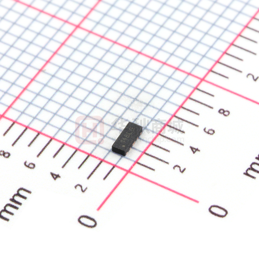
TPD1E05U06
X1SON (2)
0.60 mm × 1.00 mm
TPD4E05U06
USON (10)
2.50 mm × 1.00 mm
TPD6E05U06
USON (14)
3.50 mm × 1.35 mm
(1) For all available packages, see the orderable addendum at
the end of the datasheet.
TPD4E05U06 Functional Block Diagram
Simplified Schematic
TPD4E05U06
4
5
GND
GND
3
1
2
8
D0+
D1+
D1-
D2+
D2-
D1+
Connector
HDMI Controller
D0-
D1D2+
D2-
GND
CLK+
CLK-
GND
GND
TPD4E05U06
3
1
2
4
5
8
1
An IMPORTANT NOTICE at the end of this data sheet addresses availability, warranty, changes, use in safety-critical applications,
intellectual property matters and other important disclaimers. PRODUCTION DATA.
�TPD1E05U06, TPD4E05U06, TPD6E05U06
SLVSBO7L – DECEMBER 2012 – REVISED JANUARY 2017
www.ti.com
Table of Contents
1
2
3
4
5
6
7
Features ..................................................................
Applications ...........................................................
Description .............................................................
Revision History.....................................................
Pin Configuration and Functions .........................
Specifications.........................................................
1
1
1
2
4
6
6.1
6.2
6.3
6.4
6.5
6.6
6.7
6
6
6
6
6
7
8
Absolute Maximum Ratings ......................................
ESD Ratings—JEDEC Specification.........................
ESD Ratings—IEC Specification ..............................
Recommended Operating Conditions.......................
Thermal Information ..................................................
Electrical Characteristics...........................................
Typical Characteristics ..............................................
Detailed Description ............................................ 10
7.1 Overview ................................................................. 10
7.2 Functional Block Diagram ....................................... 10
7.3 Feature Description................................................. 11
7.4 Device Functional Modes........................................ 11
8
Application and Implementation ........................ 12
8.1 Application Information............................................ 12
8.2 Typical Applications ................................................ 12
9 Power Supply Recommendations...................... 16
10 Layout................................................................... 16
10.1 Layout Guidelines ................................................. 16
10.2 Layout Example .................................................... 16
11 Device and Documentation Support ................. 18
11.1
11.2
11.3
11.4
11.5
11.6
11.7
Documentation Support ........................................
Related Links ........................................................
Receiving Notification of Documentation Updates
Community Resources..........................................
Trademarks ...........................................................
Electrostatic Discharge Caution ............................
Glossary ................................................................
18
18
18
18
18
18
19
12 Mechanical, Packaging, and Orderable
Information ........................................................... 19
4 Revision History
NOTE: Page numbers for previous revisions may differ from page numbers in the current version.
Changes from Revision K (November 2016) to Revision L
Page
•
Updated DPY pinout image. ................................................................................................................................................... 4
•
Updated title from TPD4E05U06 to TPD6E05U06 in Figure 13 .......................................................................................... 10
Changes from Revision J (March 2016) to Revision K
•
Page
Changed min value of VBR from "6 V" to "6.5 V" in the Electrical Characteristics table......................................................... 7
Changes from Revision I (June 2015) to Revision J
Page
•
Replaced all instances of X2SON with X1SON...................................................................................................................... 1
•
Update the Pin Functions table ............................................................................................................................................. 4
•
Added Power Supply Recommendations section................................................................................................................. 16
Changes from Revision H (May 2015) to Revision I
Page
•
Added Trademarks ................................................................................................................................................................ 1
•
Corrected TPD6E05U06 Pin 13 name ................................................................................................................................... 5
•
Corrected TLP definition ........................................................................................................................................................ 7
Changes from Revision G (July 2014) to Revision H
Page
•
Added Additional Application.................................................................................................................................................. 1
•
Updated with HDMI 2.0 Eye Diagrams................................................................................................................................. 13
2
Submit Documentation Feedback
Copyright © 2012–2017, Texas Instruments Incorporated
Product Folder Links: TPD1E05U06 TPD4E05U06 TPD6E05U06
�TPD1E05U06, TPD4E05U06, TPD6E05U06
www.ti.com
SLVSBO7L – DECEMBER 2012 – REVISED JANUARY 2017
Changes from Revision F (November 2013) to Revision G
Page
•
Added 61000-4-4 EFT compliance......................................................................................................................................... 1
•
Added Handling Ratings table. ............................................................................................................................................... 6
•
Added Thermal Information table. ......................................................................................................................................... 6
•
Added Detailed Description section. .................................................................................................................................... 10
•
Added Application and Implementation section. ................................................................................................................. 12
•
Added Layout section. ......................................................................................................................................................... 16
Changes from Original (December 2012) to Revision A
•
Page
Added TPS2EUSB30A part to document. .............................................................................................................................. 1
Changes from Revision A (December 2012) to Revision B
Page
•
Added Insertion Loss Graphic. ............................................................................................................................................... 9
•
Added Eye Diagrams............................................................................................................................................................ 13
Changes from Revision B (January 2013) to Revision C
Page
•
Changed IO Capacitance range ............................................................................................................................................. 1
•
Changed test conditions and typ values for Vclamp ................................................................................................................. 7
•
Added typ RDYN values for DQA and RVZ packages ............................................................................................................. 7
•
Added CL values for DQA and RVZ packages ....................................................................................................................... 7
•
Changed CURRENT vs VOLTAGE graphic ........................................................................................................................... 8
•
Changed Insertion Loss graphic............................................................................................................................................. 9
•
Changed HDMI Eye Diagrams ............................................................................................................................................. 13
Changes from Revision C (March 2013) to Revision D
Page
•
Updated Title. ......................................................................................................................................................................... 1
•
Removed Ordering Information table. .................................................................................................................................... 4
Changes from Revision D (August 2013) to Revision E
Page
•
Updated document formatting. ............................................................................................................................................... 1
•
Added additional application................................................................................................................................................... 1
Copyright © 2012–2017, Texas Instruments Incorporated
Submit Documentation Feedback
Product Folder Links: TPD1E05U06 TPD4E05U06 TPD6E05U06
3
�TPD1E05U06, TPD4E05U06, TPD6E05U06
SLVSBO7L – DECEMBER 2012 – REVISED JANUARY 2017
www.ti.com
5 Pin Configuration and Functions
DPY Package
2-Pin X1SON
Top View
DQA Package
10-Pin USON
Top View
I/O
D1+
1
10
NC
D1–
2
9
NC
GND
3
8
GND
D2+
4
7
NC
D2–
5
6
NC
1
2
GND
RVZ Package
14-Pin USON
Top View
NC
1
14
D1+
NC
2
13
D1–
NC
3
12
D2+
NC
4
11
D2–
GND
5
10
GND
NC
6
9
D3+
NC
7
8
D3–
Pin Functions TPD1E05U06 DPY
PIN
NAME
NO.
TYPE
GND
2
Ground
I/O
1
I/O
(1)
DESCRIPTION
Ground; Connect to ground
ESD protected channel (1)
Place as close to the connector as possible.
Pin Functions TPD4E05U06 DQA
PIN
NAME
NO.
TYPE
DESCRIPTION
D1+
1
I/O
ESD protected channel (1)
D1–
2
I/O
ESD protected channel (1)
D2+
4
I/O
ESD protected channel (1)
D2–
5
I/O
ESD protected channel (1)
(1)
4
Place as close to the connector as possible.
Submit Documentation Feedback
Copyright © 2012–2017, Texas Instruments Incorporated
Product Folder Links: TPD1E05U06 TPD4E05U06 TPD6E05U06
�TPD1E05U06, TPD4E05U06, TPD6E05U06
www.ti.com
SLVSBO7L – DECEMBER 2012 – REVISED JANUARY 2017
Pin Functions TPD4E05U06 DQA (continued)
PIN
NAME
NO.
GND
3
GND
8
NC
6
NC
7
NC
9
NC
10
TYPE
Ground
—
DESCRIPTION
Ground; Connect to ground
Not connected; Used for optional straight-through routing. Can be left floating or grounded
Pin Functions TPD6E05U06 RVZ
PIN
NAME
NO.
TYPE
DESCRIPTION
D1+
14
I/O
ESD protected channel (1)
D1–
13
I/O
ESD protected channel (1)
D2+
12
I/O
ESD protected channel (1)
D2–
11
I/O
ESD protected channel (1)
D3+
9
I/O
ESD protected channel (1)
D3–
8
I/O
ESD protected channel (1)
GND
5
GND
10
NC
1
NC
2
NC
3
NC
4
NC
6
NC
7
(1)
Ground
—
Ground; Connect to ground
Not connected; Used for optional straight-through routing. Can be left floating or grounded
Place as close to the connector as possible.
Copyright © 2012–2017, Texas Instruments Incorporated
Submit Documentation Feedback
Product Folder Links: TPD1E05U06 TPD4E05U06 TPD6E05U06
5
�TPD1E05U06, TPD4E05U06, TPD6E05U06
SLVSBO7L – DECEMBER 2012 – REVISED JANUARY 2017
www.ti.com
6 Specifications
6.1 Absolute Maximum Ratings (1) (2) (3)
over operating free-air temperature range (unless otherwise noted)
MIN
Electrical fast
transient
Peak pulse
IEC 61000-4-4 (5/50 ns)
IEC 61000-4-5 Current (tp – 8/20 µs)
(4)
IEC 61000-4-5 Power (tp – 8/20 µs) (4)
MAX
UNIT
80
A
2.5
A
40
W
TA
Operating temperature
–40
125
°C
Tstg
Storage temperature
–65
155
°C
(1)
(2)
(3)
(4)
Stresses beyond those listed under absolute maximum ratings may cause permanent damage to the device. These are stress ratings
only and functional operation of the device at these or any other conditions beyond those indicated under recommended operating
conditions is not implied. Exposure to absolute-maximum-rated conditions for extended periods may affect device reliability.
Absolute maximum ratings apply over recommended junction temperature range.
Voltages are with respect to GND unless otherwise noted.
Measured at 25°C.
6.2 ESD Ratings—JEDEC Specification
VALUE
V(ESD)
(1)
(2)
Electrostatic discharge
Human-body model (HBM), per ANSI/ESDA/JEDEC JS-001
(1)
UNIT
±4000
Charged-device model (CDM), per JEDEC specification JESD22-C101 (2)
V
±1500
JEDEC document JEP155 states that 500-V HBM allows safe manufacturing with a standard ESD control process. Manufacturing with
less than 500-V HBM is possible with the necessary precautions. Pins listed as ±4000 V may actually have higher performance.
JEDEC document JEP157 states that 250-V CDM allows safe manufacturing with a standard ESD control process. Manufacturing with
less than 250-V CDM is possible with the necessary precautions. Pins listed as ±1500 V may actually have higher performance.
6.3 ESD Ratings—IEC Specification
VALUE
V(ESD)
Electrostatic discharge
IEC 61000-4-2 contact discharge
±12000
IEC 61000-4-2 air-gap discharge
±15000
UNIT
V
6.4 Recommended Operating Conditions
over operating free-air temperature range (unless otherwise noted)
VIO
Input pin voltage
TA
Operating free-air temperature
MIN
MAX
0
5.5
UNIT
V
–40
125
°C
6.5 Thermal Information
THERMAL METRIC (1)
TPD1E05U06
TPD4E05U06
TPD6E05U06
DPY (X1SON)
DQA (USON)
RVZ (USON)
2 PINS
10 PINS
14 PINS
697.3
327
197.9
°C/W
UNIT
RθJA
Junction-to-ambient thermal resistance
RθJC(top)
Junction-to-case (top) thermal resistance
471
189.5
119.1
°C/W
RθJB
Junction-to-board thermal resistance
575.9
257.7
92.6
°C/W
ψJT
Junction-to-top characterization parameter
175.7
60.9
22
°C/W
ψJB
Junction-to-board characterization parameter
575.1
257
91.6
°C/W
(1)
6
For more information about traditional and new thermal metrics, see the Semiconductor and IC Package Thermal Metrics application
report.
Submit Documentation Feedback
Copyright © 2012–2017, Texas Instruments Incorporated
Product Folder Links: TPD1E05U06 TPD4E05U06 TPD6E05U06
�TPD1E05U06, TPD4E05U06, TPD6E05U06
www.ti.com
SLVSBO7L – DECEMBER 2012 – REVISED JANUARY 2017
6.6 Electrical Characteristics
over operating free-air temperature range (unless otherwise noted)
PARAMETER
TEST CONDITIONS
VRWM
Reverse stand-off voltage
IIO < 10 µA
VBR
Break-down voltage
IIO = 1 mA
Vclamp
Clamp voltage
MIN
6.5
I = 1 A, TLP, I/O to ground (1)
10
I = 5 A, TLP, I/O to ground (1)
14
(1)
3
I = 1 A, TLP, ground to I/O
I = 5 A, TLP, ground to I/O (1)
ILEAK
RDYN
Leakage current
TYP
UNIT
5.5
V
8.5
V
V
7
VIO = 2.5 V
0.01
(2)
0.8
DPY package dynamic
resistance
I/O to GND
GND to I/O (2)
0.8
DQA package dynamic
resistance
I/O to GND (2)
0.8
(2)
0.8
RVZ package dynamic
resistance
I/O to GND (2)
0.8
GND to I/O (2)
0.8
GND to I/O
MAX
10
nA
Ω
Ω
Ω
Capacitance
ΔCIO-TOGND
CCROSS
(1)
(2)
(3)
VIO = 2.5 V, f = 1 MHz,
I/O to GND
Line capacitance (3)
CL
TPD1E05U06 DPY
package
0.42
TPD4E05U06 DQA
package
0.5
TPD6E05U06 RVZ
package
0.47
pF
Variation of channel input
capacitance
GND Pin = 0 V, F = 1 GHz, VBIAS = 2.5 V,
channel_x pin to GND – channel_y pin to GND
0.05
0.07
pF
Channel to channel input
capacitance
GND Pin = 0 V, F = 1 GHz, VBIAS = 2.5 V, between
channel pins
0.01
0.06
pF
Transmission Line Pulse (TLP) with 100 ns width, 200 ps rise time.
Extraction of RDYN using least squares fit of TLP characteristics between I = 10 A and I = 20 A.
Capacitance data is taken at 25°C.
Copyright © 2012–2017, Texas Instruments Incorporated
Submit Documentation Feedback
Product Folder Links: TPD1E05U06 TPD4E05U06 TPD6E05U06
7
�TPD1E05U06, TPD4E05U06, TPD6E05U06
SLVSBO7L – DECEMBER 2012 – REVISED JANUARY 2017
www.ti.com
6.7 Typical Characteristics
3.5
1.0
0.8
50
Current
Power
3.0
45
40
0.6
2.5
0.2
0.0
±0.2
±0.4
35
Power (W)
Current (A)
Current (mA)
0.4
30
2.0
25
1.5
20
15
1.0
10
±0.6
0.5
±0.8
5
0
0.0
±1.0
±2
0
±1
1
2
3
4
5
6
7
8
9
Voltage (V)
10
0
±5
5
10
15
20
25
30
35
40
45
50
Time ( s)
C001
Figure 1. DC Voltage Sweep I-V Curve
C002
Figure 2. Surge Curve (tp = 8/20 μs), Pin IO to GND
25
35
30
20
20
Current (A)
Current (A)
25
15
10
5
15
10
5
0
0
±5
0
5
10
15
20
25
30
35
Voltage (V)
0
40
5
10
15
20
25
Voltage (V)
C003
Figure 3. Positive TLP Plot IO to GND
C008
Figure 4. Negative TLP Plot IO to GND
300
80
70
250
Voltage (V)
Current (pA)
60
200
150
100
50
40
30
20
10
50
0
0
±10
±40
±20
0
20
40
60
80
100
Temperature (ƒC)
Figure 5. Leakage vs Temperature
8
Submit Documentation Feedback
120
0
25
50
75
100
125
150
Time (ns)
C004
175
200
C005
Figure 6. 8-kV IEC Waveform
Copyright © 2012–2017, Texas Instruments Incorporated
Product Folder Links: TPD1E05U06 TPD4E05U06 TPD6E05U06
�TPD1E05U06, TPD4E05U06, TPD6E05U06
www.ti.com
SLVSBO7L – DECEMBER 2012 – REVISED JANUARY 2017
Typical Characteristics (continued)
10
0
0
±1
±2
±10
±3
Insertion Loss (dB)
Voltage (V)
±20
±30
±40
±50
±60
±4
±5
±6
±7
±8
±9
±70
±10
±80
±11
±90
0
25
50
75
100
125
150
175
Time (ns)
200
±12
100k
Figure 7. –8-kV IEC Waveform
100M
1G
1000M
10G
10000M
C007
Figure 8. TPD1E05U06 Insertion Loss
0
±1
±1
Insertion Loss (dB)
Insertion Loss (dB)
10M
Frequency (Hz)
0
±2
±3
±4
±5
±6
100k
1M
C006
±2
±3
±4
±5
1M
10M
100M
1G
1000M
Frequency (Hz)
Figure 9. TPD4E05U06 Insertion Loss
Copyright © 2012–2017, Texas Instruments Incorporated
10G
10000M
C009
±6
100k
1M
10M
100M
1G
1000M
10G
10000M
Frequency (Hz)
C010
Figure 10. TPD6E05U06 Insertion Loss
Submit Documentation Feedback
Product Folder Links: TPD1E05U06 TPD4E05U06 TPD6E05U06
9
�TPD1E05U06, TPD4E05U06, TPD6E05U06
SLVSBO7L – DECEMBER 2012 – REVISED JANUARY 2017
www.ti.com
7 Detailed Description
7.1 Overview
The TPDxE05U06 is a family of unidirectional Transient Voltage Suppressor (TVS) based Electrostatic Discharge
(ESD) protection diodes with ultra-low capacitance. Each device can dissipate ESD strikes above the maximum
level specified by the IEC 61000-4-2 international standard. The TPDxE05U06s ultra-low loading capacitance
makes it ideal for protecting any high-speed signal pins.
7.2 Functional Block Diagram
I/O
GND
Figure 11. TPD1E05U06 Block Diagram
D1+
D1-
D2+
D2-
GND
Figure 12. TPD4E05U06 Block Diagram
D1+
D1-
D2+
D2-
D3+
D3-
GND
Figure 13. TPD6E05U06 Block Diagram
10
Submit Documentation Feedback
Copyright © 2012–2017, Texas Instruments Incorporated
Product Folder Links: TPD1E05U06 TPD4E05U06 TPD6E05U06
�TPD1E05U06, TPD4E05U06, TPD6E05U06
www.ti.com
SLVSBO7L – DECEMBER 2012 – REVISED JANUARY 2017
7.3 Feature Description
The TPDxE05U06 is a family of unidirectional Transient Voltage Suppressor (TVS) Electrostatic Discharge (ESD)
protection diodes with ultra-low capacitance. Each device can dissipate ESD strikes above the maximum level
specified by the IEC 61000-4-2 international standard. The TPDxE05U06s ultra-low loading capacitance makes it
ideal for protecting any high-speed signal pins.
7.3.1 ±15-kV IEC61000-4-2 Level 4 ESD Protection
The I/O pins can withstand ESD events up to ±12-kV contact and ±15-kV air. An ESD-surge clamp diverts the
current to ground.
7.3.2 IEC61000-4-4 EFT Protection
The I/O pins can withstand an electrical fast transient burst of up to 80 A (5/50 ns waveform, 4 kV with 50-Ω
impedance). An ESD-surge clamp diverts the current to ground. This has been validated on the TPD4E05U06
only.
7.3.3 IEC61000-4-5 Surge Protection
The I/O pins can withstand surge events up to 2.5 A and 40 W (8/20 µs waveform). An ESD-surge clamp diverts
this current to ground.
7.3.4 I/O Capacitance
The capacitance between each I/O pin to ground is 0.42 pF (TPD1E05U06), 0.5 pF (TPD4E05U06) or 0.47 pF
(TPD6E05U06). These devices support data rates up to 6 Gbps.
7.3.5 DC Breakdown Voltage
The DC breakdown voltage of each I/O pin is a minimum of 6 V. This ensures that sensitive equipment is
protected from surges above the reverse standoff voltage of 5 V.
7.3.6 Ultra-Low Leakage Current
The I/O pins feature an ultra-low leakage current of 10 nA (max) with a bias of 2.5 V.
7.3.7 Low ESD Clamping Voltage
The I/O pins feature an ESD clamp that is capable of clamping the voltage to 10 V (IPP = 1 A).
7.3.8 Industrial Temperature Range
This device features an industrial operating range of –40°C to +125°C.
7.3.9 Easy Flow-Through Routing
The layout of this device makes it simple and easy to add protection to an existing layout. The packages offers
flow-through routing, requiring minimal modification to an existing layout.
7.4 Device Functional Modes
The TPDxE05U06 is a passive integrated circuit that triggers when voltages are above VBR or below the lower
diodes Vf (–0.6 V). During ESD events, voltages as high as ±15 kV (air) can be directed to ground via the internal
diode network. When the voltages on the protected line fall below the trigger levels of TPDxE05U06 (usually
within 10s of nano-seconds) the device reverts to passive.
Copyright © 2012–2017, Texas Instruments Incorporated
Submit Documentation Feedback
Product Folder Links: TPD1E05U06 TPD4E05U06 TPD6E05U06
11
�TPD1E05U06, TPD4E05U06, TPD6E05U06
SLVSBO7L – DECEMBER 2012 – REVISED JANUARY 2017
www.ti.com
8 Application and Implementation
NOTE
Information in the following applications sections is not part of the TI component
specification, and TI does not warrant its accuracy or completeness. TI’s customers are
responsible for determining suitability of components for their purposes. Customers should
validate and test their design implementation to confirm system functionality.
8.1 Application Information
The TPDxE05U06 is a diode type TVS which is typically used to provide a path to ground for dissipating ESD
events on hi-speed signal lines between a human interface connector and a system. As the current from ESD
passes through the TVS, only a small voltage drop is present across the diode. This is the voltage presented to
the protected IC. The low RDYN of the triggered TVS holds this voltage, VCLAMP, to a safe level for the protected
IC.
8.2 Typical Applications
8.2.1 HDMI 2.0 Application
TPD4E05U06DQA
HOT PLUG 1
UTILITY 2
D2+
1
10
D2-
2
9
3
8
4
7
5
6
UTI_CON
TMDS D2+ 3
D2-
5V Source
D1+
D1+
TMDS_GND 4
D2+
D1-
D1-
TMDS D2- 5
HDMI Connector
TMDS D1+ 6
TPD4E05U06DQA
TMDS_GND 7
TMDS D1- 8
D0+
1
10
D0-
2
9
3
8
4
7
5
6
D0+
D0-
TMDS D0+ 9
TMDS_GND 10
CLK+
TMDS D0- 11
CLK-
CLK+
CLK-
TMDS CLK+ 12
TMDS_GND 13
TPD5S116YFF
TMDS CLK- 14
CEC 15
CEC_CON
DDC/CEC GND 16
SCL_CON
SCL 17
SDA_CON
SDA 18
EN
GND 20
SDA_SYS
5V_SYS
HPD_CON
0.1 µF
SCL_SYS
VCCA
5V_CON
P 5V0 19
HDMI Controller
CEC_SYS
UTI_CON
HPD_SYS
GND
0.1 µF
UTI_CON
Figure 14. HDMI 2.0 Schematic
12
Submit Documentation Feedback
Copyright © 2012–2017, Texas Instruments Incorporated
Product Folder Links: TPD1E05U06 TPD4E05U06 TPD6E05U06
�TPD1E05U06, TPD4E05U06, TPD6E05U06
www.ti.com
SLVSBO7L – DECEMBER 2012 – REVISED JANUARY 2017
Typical Applications (continued)
8.2.1.1 Design Requirements
For this design example, the two TPD4E05U06 devices, and a TPD5S116 are being used in an HDMI 2.0
application. This provides a complete port protection scheme.
Given the HDMI 2.0 application, the parameters listed in Table 1 are known.
Table 1. Design Parameters
DESIGN PARAMETER
VALUE
Signal range on pins 1, 2, 4, or 5
0 V to 5 V
Operating frequency
3 GHz
8.2.1.2 Detailed Design Procedure
8.2.1.2.1 Signal Range on Pin 1, 2, 4, or 5
The TPD4E05U06 has 4 identical protection channels for signal lines. The symmetry of the device provides
flexibility when selecting which of the 4 I/O channels is going to protect which signal lines. Any I/O supports a
signal range of 0 to 5.5 V.
8.2.1.3 Application Curves
Figure 15. 3.4-Gbps HDMI 1.4 TP1 Eye Diagram
Unpopulated EVM
Figure 16. 3.4-Gbps HDMI 1.4 TP1 Eye Diagram
TPD1E05U06
Figure 17. 3.4-Gbps HDMI 1.4 TP1 Eye Diagram
TPD4E05U06
Figure 18. 3.4-Gbps HDMI 1.4 TP1 Eye Diagram
TPD6E05U06
Copyright © 2012–2017, Texas Instruments Incorporated
Submit Documentation Feedback
Product Folder Links: TPD1E05U06 TPD4E05U06 TPD6E05U06
13
�TPD1E05U06, TPD4E05U06, TPD6E05U06
SLVSBO7L – DECEMBER 2012 – REVISED JANUARY 2017
www.ti.com
Figure 19. 6-Gbps HDMI 2.0 (TP1) Eye Diagram
Unpopulated EVM
Figure 20. 6-Gbps HDMI 2.0 (TP1) Eye Diagram
TPD1E05U06
Figure 21. 6-Gbps HDMI 2.0 (TP1) Eye Diagram
TPD4E05U06
Figure 22. 6-Gbps HDMI 2.0 (TP1) Eye Diagram
TPD6E05U06
8.2.2 HDMI 2.0 Application
1
TPD1E05U06
1
TPD1E05U06
1
TPD1E05U06
2
1
GND
2
GND
GND
GND
TPD1E05U06
2
2
D0D1+
Connector
HDMI 2.0 Controller
D0+
D1D2+
D2CLK+
CLK1
TPD1E05U06
1
2
GND
2
1
TPD1E05U06
GND
2
1
TPD1E05U06
GND
GND
TPD1E05U06
2
Figure 23. HDMI 2.0 Schematic
14
Submit Documentation Feedback
Copyright © 2012–2017, Texas Instruments Incorporated
Product Folder Links: TPD1E05U06 TPD4E05U06 TPD6E05U06
�TPD1E05U06, TPD4E05U06, TPD6E05U06
www.ti.com
SLVSBO7L – DECEMBER 2012 – REVISED JANUARY 2017
8.2.2.1 Design Requirements
For this design example, the TPD1E05U06 and the TPD5S116 are used to protect the data pairs and control
lines of the HDMI 2.0 connection. This provides full HDMI 2.0 port protection.
Given the HDMI 2.0 application, the following parameters in Table 2 are known.
Table 2. Design Parameters
DESIGN PARAMETER
VALUE
Signal range on data lines
0 V to 5 V
Operating frequency
3 GHz
8.2.2.2 Detailed Design Procedure
8.2.2.2.1 Signal Range
The TPD1E05U06 has 1 protection channel for signal lines, supporting a signal range of 0 V to 5.5 V.
8.2.2.2.2 Operating Frequency
The TPD1E05U06 has 0.42 pF of capacitance, which supports HDMI 2.0 data rates.
8.2.2.3 Application Curves
Refer to the Application Curves section.
Copyright © 2012–2017, Texas Instruments Incorporated
Submit Documentation Feedback
Product Folder Links: TPD1E05U06 TPD4E05U06 TPD6E05U06
15
�TPD1E05U06, TPD4E05U06, TPD6E05U06
SLVSBO7L – DECEMBER 2012 – REVISED JANUARY 2017
www.ti.com
9 Power Supply Recommendations
This device is a passive ESD protection device and there is no need to power it. Care must be taken to make
sure that the maximum voltage specifications for each line are not violated.
10 Layout
10.1 Layout Guidelines
•
•
•
The optimum placement is as close to the connector as possible.
– EMI during an ESD event can couple from the trace being struck to other nearby unprotected traces,
resulting in early system failures.
– The PCB designer needs to minimize the possibility of EMI coupling by keeping any unprotected traces
away from the protected traces which are between the TVS and the connector.
Route the protected traces as straight as possible.
Eliminate any sharp corners on the protected traces between the TVS and the connector by using rounded
corners with the largest radii possible.
– Electric fields tend to build up on corners, increasing EMI coupling.
10.2 Layout Example
10.2.1 TPD4E05U06 Layout Example
This application is typical of an HDMI 1.4 layout.
Clk+
Clk-
D0+
D0-
D1+
D1-
D2+
D2-
VIA to GND Plane
D0+
NC
NC
NC
D1-
NC
D0-
D0+
NC
GND
D0-
GND
GND
GND
NC
NC
D1+
NC
D1+
D1-
Figure 24. TPD4E05U06 Layout
16
Submit Documentation Feedback
Copyright © 2012–2017, Texas Instruments Incorporated
Product Folder Links: TPD1E05U06 TPD4E05U06 TPD6E05U06
�TPD1E05U06, TPD4E05U06, TPD6E05U06
www.ti.com
SLVSBO7L – DECEMBER 2012 – REVISED JANUARY 2017
Layout Example (continued)
10.2.2 TPD1E05U06 Layout Example
This application is typical of an HDMI 2.0 layout.
Clk+
Clk-
GND
GND
I/O
I/O
D0+
D0I/O
GND
I/O
I/O
GND
I/O
GND
I/O
GND
I/O
GND
GND
D2+
D2-
D1+
D1-
VIA to GND Plane
Figure 25. TPD1E05U06 Layout
Copyright © 2012–2017, Texas Instruments Incorporated
Submit Documentation Feedback
Product Folder Links: TPD1E05U06 TPD4E05U06 TPD6E05U06
17
�TPD1E05U06, TPD4E05U06, TPD6E05U06
SLVSBO7L – DECEMBER 2012 – REVISED JANUARY 2017
www.ti.com
11 Device and Documentation Support
11.1 Documentation Support
11.1.1 Related Documentation
For related documentation see the following:
• Reading and Understanding an ESD Protection Datasheet
• ESD Layout Guide
• TPD6E05U06RVZ EVM User's Guide
• Picking ESD Diodes for Ultra High-Speed Data Lines
• ESD PROTECTION DIODES EVM
• TPD1E05U06DPY EVM User's Guide
• TPD4E05U06DQA EVM User's Guide
11.2 Related Links
The table below lists quick access links. Categories include technical documents, support and community
resources, tools and software, and quick access to sample or buy.
Table 3. Related Links
PARTS
PRODUCT FOLDER
SAMPLE & BUY
TECHNICAL
DOCUMENTS
TOOLS &
SOFTWARE
SUPPORT &
COMMUNITY
TPD1E05U06
Click here
Click here
Click here
Click here
Click here
TPD4E05U06
Click here
Click here
Click here
Click here
Click here
TPD6E05U06
Click here
Click here
Click here
Click here
Click here
11.3 Receiving Notification of Documentation Updates
To receive notification of documentation updates—including silicon errata—go to the product folder for your
device on ti.com. In the upper right-hand corner, click the Alert me button. This registers you to receive a weekly
digest of product information that has changed (if any). For change details, check the revision history of any
revised document.
11.4 Community Resources
The following links connect to TI community resources. Linked contents are provided "AS IS" by the respective
contributors. They do not constitute TI specifications and do not necessarily reflect TI's views; see TI's Terms of
Use.
TI E2E™ Online Community TI's Engineer-to-Engineer (E2E) Community. Created to foster collaboration
among engineers. At e2e.ti.com, you can ask questions, share knowledge, explore ideas and help
solve problems with fellow engineers.
Design Support TI's Design Support Quickly find helpful E2E forums along with design support tools and
contact information for technical support.
11.5 Trademarks
E2E is a trademark of Texas Instruments.
PCI-Express is a registered trademark of PCI-SIG .
V-by-One is a registered trademark of Thine Electronics, Inc.
All other trademarks are the property of their respective owners.
11.6 Electrostatic Discharge Caution
These devices have limited built-in ESD protection. The leads should be shorted together or the device placed in conductive foam
during storage or handling to prevent electrostatic damage to the MOS gates.
18
Submit Documentation Feedback
Copyright © 2012–2017, Texas Instruments Incorporated
Product Folder Links: TPD1E05U06 TPD4E05U06 TPD6E05U06
�TPD1E05U06, TPD4E05U06, TPD6E05U06
www.ti.com
SLVSBO7L – DECEMBER 2012 – REVISED JANUARY 2017
11.7 Glossary
SLYZ022 — TI Glossary.
This glossary lists and explains terms, acronyms, and definitions.
12 Mechanical, Packaging, and Orderable Information
The following pages include mechanical, packaging, and orderable information. This information is the most
current data available for the designated devices. This data is subject to change without notice and revision of
this document. For browser-based versions of this data sheet, refer to the left-hand navigation.
Copyright © 2012–2017, Texas Instruments Incorporated
Submit Documentation Feedback
Product Folder Links: TPD1E05U06 TPD4E05U06 TPD6E05U06
19
�PACKAGE OPTION ADDENDUM
www.ti.com
7-Nov-2016
PACKAGING INFORMATION
Orderable Device
Status
(1)
Package Type Package Pins Package
Drawing
Qty
Eco Plan
Lead/Ball Finish
MSL Peak Temp
(2)
(6)
(3)
Op Temp (°C)
Device Marking
(4/5)
TPD1E05U06DPYR
ACTIVE
X1SON
DPY
2
10000
Green (RoHS
& no Sb/Br)
CU NIPDAU
Level-1-260C-UNLIM
-40 to 125
(C1 ~ C6)
TPD1E05U06DPYT
ACTIVE
X1SON
DPY
2
250
Green (RoHS
& no Sb/Br)
CU NIPDAU
Level-1-260C-UNLIM
-40 to 125
(C1 ~ C6)
TPD4E05U06DQAR
ACTIVE
USON
DQA
10
3000
Green (RoHS
& no Sb/Br)
CU NIPDAU
Level-1-260C-UNLIM
-40 to 125
BR
BRY
TPD6E05U06RVZR
ACTIVE
USON
RVZ
14
3000
Green (RoHS
& no Sb/Br)
CU NIPDAU
Level-1-260C-UNLIM
-40 to 125
(BV ~ BVY)
(1)
The marketing status values are defined as follows:
ACTIVE: Product device recommended for new designs.
LIFEBUY: TI has announced that the device will be discontinued, and a lifetime-buy period is in effect.
NRND: Not recommended for new designs. Device is in production to support existing customers, but TI does not recommend using this part in a new design.
PREVIEW: Device has been announced but is not in production. Samples may or may not be available.
OBSOLETE: TI has discontinued the production of the device.
(2)
Eco Plan - The planned eco-friendly classification: Pb-Free (RoHS), Pb-Free (RoHS Exempt), or Green (RoHS & no Sb/Br) - please check http://www.ti.com/productcontent for the latest availability
information and additional product content details.
TBD: The Pb-Free/Green conversion plan has not been defined.
Pb-Free (RoHS): TI's terms "Lead-Free" or "Pb-Free" mean semiconductor products that are compatible with the current RoHS requirements for all 6 substances, including the requirement that
lead not exceed 0.1% by weight in homogeneous materials. Where designed to be soldered at high temperatures, TI Pb-Free products are suitable for use in specified lead-free processes.
Pb-Free (RoHS Exempt): This component has a RoHS exemption for either 1) lead-based flip-chip solder bumps used between the die and package, or 2) lead-based die adhesive used between
the die and leadframe. The component is otherwise considered Pb-Free (RoHS compatible) as defined above.
Green (RoHS & no Sb/Br): TI defines "Green" to mean Pb-Free (RoHS compatible), and free of Bromine (Br) and Antimony (Sb) based flame retardants (Br or Sb do not exceed 0.1% by weight
in homogeneous material)
(3)
MSL, Peak Temp. - The Moisture Sensitivity Level rating according to the JEDEC industry standard classifications, and peak solder temperature.
(4)
There may be additional marking, which relates to the logo, the lot trace code information, or the environmental category on the device.
(5)
Multiple Device Markings will be inside parentheses. Only one Device Marking contained in parentheses and separated by a "~" will appear on a device. If a line is indented then it is a continuation
of the previous line and the two combined represent the entire Device Marking for that device.
(6)
Lead/Ball Finish - Orderable Devices may have multiple material finish options. Finish options are separated by a vertical ruled line. Lead/Ball Finish values may wrap to two lines if the finish
value exceeds the maximum column width.
Addendum-Page 1
Samples
�PACKAGE OPTION ADDENDUM
www.ti.com
7-Nov-2016
Important Information and Disclaimer:The information provided on this page represents TI's knowledge and belief as of the date that it is provided. TI bases its knowledge and belief on information
provided by third parties, and makes no representation or warranty as to the accuracy of such information. Efforts are underway to better integrate information from third parties. TI has taken and
continues to take reasonable steps to provide representative and accurate information but may not have conducted destructive testing or chemical analysis on incoming materials and chemicals.
TI and TI suppliers consider certain information to be proprietary, and thus CAS numbers and other limited information may not be available for release.
In no event shall TI's liability arising out of such information exceed the total purchase price of the TI part(s) at issue in this document sold by TI to Customer on an annual basis.
OTHER QUALIFIED VERSIONS OF TPD1E05U06, TPD4E05U06 :
• Automotive: TPD1E05U06-Q1, TPD4E05U06-Q1
NOTE: Qualified Version Definitions:
• Automotive - Q100 devices qualified for high-reliability automotive applications targeting zero defects
Addendum-Page 2
�PACKAGE MATERIALS INFORMATION
www.ti.com
29-Aug-2017
TAPE AND REEL INFORMATION
*All dimensions are nominal
Device
Package Package Pins
Type Drawing
SPQ
Reel
Reel
A0
Diameter Width (mm)
(mm) W1 (mm)
B0
(mm)
K0
(mm)
P1
(mm)
W
Pin1
(mm) Quadrant
TPD1E05U06DPYR
X1SON
DPY
2
10000
180.0
9.5
0.66
1.15
0.66
2.0
8.0
Q1
TPD1E05U06DPYR
X1SON
DPY
2
10000
180.0
9.5
0.72
1.12
0.43
2.0
8.0
Q1
TPD1E05U06DPYT
X1SON
DPY
2
250
180.0
9.5
0.66
1.15
0.66
2.0
8.0
Q1
TPD1E05U06DPYT
X1SON
DPY
2
250
180.0
9.5
0.72
1.12
0.43
2.0
8.0
Q1
TPD4E05U06DQAR
USON
DQA
10
3000
180.0
9.5
1.23
2.7
0.7
4.0
8.0
Q1
TPD4E05U06DQAR
USON
DQA
10
3000
180.0
9.5
1.18
2.68
0.72
4.0
8.0
Q1
TPD6E05U06RVZR
USON
RVZ
14
3000
178.0
13.5
1.6
3.75
0.7
4.0
12.0
Q1
TPD6E05U06RVZR
USON
RVZ
14
3000
180.0
13.2
1.65
3.8
0.7
4.0
12.0
Q1
Pack Materials-Page 1
�PACKAGE MATERIALS INFORMATION
www.ti.com
29-Aug-2017
*All dimensions are nominal
Device
Package Type
Package Drawing
Pins
SPQ
Length (mm)
Width (mm)
Height (mm)
TPD1E05U06DPYR
X1SON
DPY
2
10000
184.0
184.0
19.0
TPD1E05U06DPYR
X1SON
DPY
2
10000
189.0
185.0
36.0
TPD1E05U06DPYT
X1SON
DPY
2
250
184.0
184.0
19.0
TPD1E05U06DPYT
X1SON
DPY
2
250
189.0
185.0
36.0
TPD4E05U06DQAR
USON
DQA
10
3000
184.0
184.0
19.0
TPD4E05U06DQAR
USON
DQA
10
3000
189.0
185.0
36.0
TPD6E05U06RVZR
USON
RVZ
14
3000
189.0
185.0
36.0
TPD6E05U06RVZR
USON
RVZ
14
3000
184.0
184.0
19.0
Pack Materials-Page 2
�������IMPORTANT NOTICE
Texas Instruments Incorporated (TI) reserves the right to make corrections, enhancements, improvements and other changes to its
semiconductor products and services per JESD46, latest issue, and to discontinue any product or service per JESD48, latest issue. Buyers
should obtain the latest relevant information before placing orders and should verify that such information is current and complete.
TI’s published terms of sale for semiconductor products (http://www.ti.com/sc/docs/stdterms.htm) apply to the sale of packaged integrated
circuit products that TI has qualified and released to market. Additional terms may apply to the use or sale of other types of TI products and
services.
Reproduction of significant portions of TI information in TI data sheets is permissible only if reproduction is without alteration and is
accompanied by all associated warranties, conditions, limitations, and notices. TI is not responsible or liable for such reproduced
documentation. Information of third parties may be subject to additional restrictions. Resale of TI products or services with statements
different from or beyond the parameters stated by TI for that product or service voids all express and any implied warranties for the
associated TI product or service and is an unfair and deceptive business practice. TI is not responsible or liable for any such statements.
Buyers and others who are developing systems that incorporate TI products (collectively, “Designers”) understand and agree that Designers
remain responsible for using their independent analysis, evaluation and judgment in designing their applications and that Designers have
full and exclusive responsibility to assure the safety of Designers' applications and compliance of their applications (and of all TI products
used in or for Designers’ applications) with all applicable regulations, laws and other applicable requirements. Designer represents that, with
respect to their applications, Designer has all the necessary expertise to create and implement safeguards that (1) anticipate dangerous
consequences of failures, (2) monitor failures and their consequences, and (3) lessen the likelihood of failures that might cause harm and
take appropriate actions. Designer agrees that prior to using or distributing any applications that include TI products, Designer will
thoroughly test such applications and the functionality of such TI products as used in such applications.
TI’s provision of technical, application or other design advice, quality characterization, reliability data or other services or information,
including, but not limited to, reference designs and materials relating to evaluation modules, (collectively, “TI Resources”) are intended to
assist designers who are developing applications that incorporate TI products; by downloading, accessing or using TI Resources in any
way, Designer (individually or, if Designer is acting on behalf of a company, Designer’s company) agrees to use any particular TI Resource
solely for this purpose and subject to the terms of this Notice.
TI’s provision of TI Resources does not expand or otherwise alter TI’s applicable published warranties or warranty disclaimers for TI
products, and no additional obligations or liabilities arise from TI providing such TI Resources. TI reserves the right to make corrections,
enhancements, improvements and other changes to its TI Resources. TI has not conducted any testing other than that specifically
described in the published documentation for a particular TI Resource.
Designer is authorized to use, copy and modify any individual TI Resource only in connection with the development of applications that
include the TI product(s) identified in such TI Resource. NO OTHER LICENSE, EXPRESS OR IMPLIED, BY ESTOPPEL OR OTHERWISE
TO ANY OTHER TI INTELLECTUAL PROPERTY RIGHT, AND NO LICENSE TO ANY TECHNOLOGY OR INTELLECTUAL PROPERTY
RIGHT OF TI OR ANY THIRD PARTY IS GRANTED HEREIN, including but not limited to any patent right, copyright, mask work right, or
other intellectual property right relating to any combination, machine, or process in which TI products or services are used. Information
regarding or referencing third-party products or services does not constitute a license to use such products or services, or a warranty or
endorsement thereof. Use of TI Resources may require a license from a third party under the patents or other intellectual property of the
third party, or a license from TI under the patents or other intellectual property of TI.
TI RESOURCES ARE PROVIDED “AS IS” AND WITH ALL FAULTS. TI DISCLAIMS ALL OTHER WARRANTIES OR
REPRESENTATIONS, EXPRESS OR IMPLIED, REGARDING RESOURCES OR USE THEREOF, INCLUDING BUT NOT LIMITED TO
ACCURACY OR COMPLETENESS, TITLE, ANY EPIDEMIC FAILURE WARRANTY AND ANY IMPLIED WARRANTIES OF
MERCHANTABILITY, FITNESS FOR A PARTICULAR PURPOSE, AND NON-INFRINGEMENT OF ANY THIRD PARTY INTELLECTUAL
PROPERTY RIGHTS. TI SHALL NOT BE LIABLE FOR AND SHALL NOT DEFEND OR INDEMNIFY DESIGNER AGAINST ANY CLAIM,
INCLUDING BUT NOT LIMITED TO ANY INFRINGEMENT CLAIM THAT RELATES TO OR IS BASED ON ANY COMBINATION OF
PRODUCTS EVEN IF DESCRIBED IN TI RESOURCES OR OTHERWISE. IN NO EVENT SHALL TI BE LIABLE FOR ANY ACTUAL,
DIRECT, SPECIAL, COLLATERAL, INDIRECT, PUNITIVE, INCIDENTAL, CONSEQUENTIAL OR EXEMPLARY DAMAGES IN
CONNECTION WITH OR ARISING OUT OF TI RESOURCES OR USE THEREOF, AND REGARDLESS OF WHETHER TI HAS BEEN
ADVISED OF THE POSSIBILITY OF SUCH DAMAGES.
Unless TI has explicitly designated an individual product as meeting the requirements of a particular industry standard (e.g., ISO/TS 16949
and ISO 26262), TI is not responsible for any failure to meet such industry standard requirements.
Where TI specifically promotes products as facilitating functional safety or as compliant with industry functional safety standards, such
products are intended to help enable customers to design and create their own applications that meet applicable functional safety standards
and requirements. Using products in an application does not by itself establish any safety features in the application. Designers must
ensure compliance with safety-related requirements and standards applicable to their applications. Designer may not use any TI products in
life-critical medical equipment unless authorized officers of the parties have executed a special contract specifically governing such use.
Life-critical medical equipment is medical equipment where failure of such equipment would cause serious bodily injury or death (e.g., life
support, pacemakers, defibrillators, heart pumps, neurostimulators, and implantables). Such equipment includes, without limitation, all
medical devices identified by the U.S. Food and Drug Administration as Class III devices and equivalent classifications outside the U.S.
TI may expressly designate certain products as completing a particular qualification (e.g., Q100, Military Grade, or Enhanced Product).
Designers agree that it has the necessary expertise to select the product with the appropriate qualification designation for their applications
and that proper product selection is at Designers’ own risk. Designers are solely responsible for compliance with all legal and regulatory
requirements in connection with such selection.
Designer will fully indemnify TI and its representatives against any damages, costs, losses, and/or liabilities arising out of Designer’s noncompliance with the terms and provisions of this Notice.
Mailing Address: Texas Instruments, Post Office Box 655303, Dallas, Texas 75265
Copyright © 2017, Texas Instruments Incorporated
�


 工商网监
湘ICP备2023018690号
工商网监
湘ICP备2023018690号
