User's Guide
SLVU471A – June 2011 – Revised June 2014
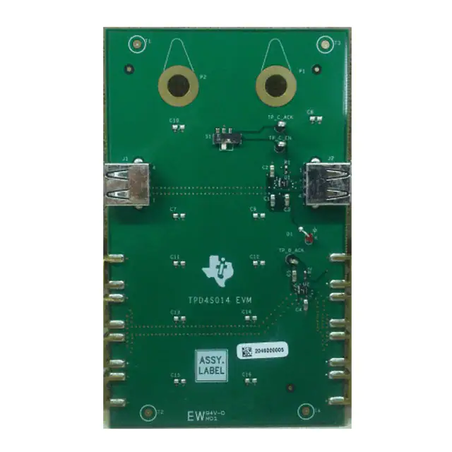
TPD4S014 EVM
Introduction
The TPD4S014 is a single-chip solution for USB
charger port protection. This device offers low
capacitance TVS type ESD clamps for the D+, D–
and standard Capacitance for the ID pin. On the
VBUS pin, this device can handle over-voltage
protection up to 28 V. The over voltage lock-out
feature ensures that, if there is a fault condition at
the VBUS line, the TPD4S014 is able to isolate
the VBUS line and protect the internal circuitry
from damage.
Similarly, the under voltage lock out feature
ensures that there is no power drain from the
internal VCC plane to external VBUS side in case
there is short to GND. There is a 16 ms turn-on
delay after VBUS crosses the under voltage
lockout threshold, in order to let the voltage
stabilize before closing the switch. This function
acts as a deglitch filter and prevents unnecessary
switching if there is any ringing on the line during
connection.
Highlighted Features
• Over-voltage protection functionality
• Under voltage lockout functionality
• USB connectors used for ease of use
• LED indicating fault condition
• Test point for EN and ACK signals
• D+, D– lines are routed as differential pair
1
EVM Description and Configuration
The TPD4S014EVM consists of four separate sections. One section is a USB2.0 pass through protected
port, one section allows 4-port analysis, one section allows ESD testing of 6 devices, and another allows
capturing a clamping waveform during an ESD event. All sections are powered up by a 1.8 V – 3.3 V
supply. This supply is used for three purposes:
1. To provide the HI and LO logic levels for the EN signal
2. To provide a pullup voltage for the open drain ACK signal
3. To power the fault indicator LED
SLVU471A – June 2011 – Revised June 2014
Submit Documentation Feedback
TPD4S014 EVM
Copyright © 2011–2014, Texas Instruments Incorporated
1
�Definitions
2
www.ti.com
Definitions
Contact Discharge — a method of testing in which the electrode of the ESD simulator is held in contact
with the device-under-test (DUT).
Air Discharge — a method of testing in which the charged electrode of the ESD simulator approaches the
DUT, and a spark to the DUT actuates the discharge.
ESD Simulator — a device that outputs IEC61000-4-2 compliance ESD waveforms shown in Figure 1 with
adjustable ranges shown in Table 1 and Table 2.
IEC61000-4-2 has 4 classes of protection levels. Classes 1 – 4 are shown in Table 1. Stress tests should
be incrementally tested to level 4 as shown in Table 2 until the point of failure. If the DUT does not fail at 8
kV, testing can continue in 2 kV increments until failure.
Table 1. IEC61000-4-2 Test Levels
Contact Discharge
Air Discharge
Class
Test Voltage [± kV]
Class
Test Voltage [± kV]
1
2
1
2
2
4
2
4
3
6
3
8
4
8
4
15
Table 2. Waveform Parameters in Contact Discharge Mode
Stress Level Step
Simulator
Voltage [kV]
Ipeak ±15% [A]
Rise Time ±25%
[nS]
Current at 30ns
±30% [A]
Current at 60ns
±30% [A]
1
2
7.5
0.8
4
2
2
4
15
0.8
8
4
3
6
22.5
0.8
12
6
4
8
30
0.8
16
8
Figure 1. Ideal Contact Discharge Waveform of the Output Current of the ESD Simulator at 4 kV
2
TPD4S014 EVM
SLVU471A – June 2011 – Revised June 2014
Submit Documentation Feedback
Copyright © 2011–2014, Texas Instruments Incorporated
�Setup
www.ti.com
3
Setup
3.1
U1
TPD4S014DSQ (U1) section has a switch to toggle the polarity of the EN signal. There are labels
indicating the ON and OFF positions of the switch. There are also test points that can be used to
determine the logic level ACK signal. This section also has an LED which indicates a fault condition.
Please note that the LED lights up when the ACK signal is at logic HI. This section is intended to illustrate
the functionality of the device without any additional test equipment. Two USB2.0 Type AB female
connectors (J2 & J3) can be used for capturing Eye Diagrams. Using either J2 as input and J3 as output,
attach to a USB2.0 compliant Eye Diagram tester setup for the intended application. For all test
procedures apply 1.8V – 3.3V to “+” of J1 and GND to “–“ of J1.
Setup Procedure
1. The fault indication LED should light up when board power is applied.
2. Connect a USB cable to the Input connector (J3). Connect a variable power supply to the VBUS line
on the other end of the cable. Set the Voltage on the power supply to < 2V.
3. Connect another USB cable to the output connector (J2) of the board. Connect a variable load to the
VBUS line on the other end of the cable. Set the load to > 25 Ω
4. Slowly increase the Voltage on the input. The LED should turn OFF when the Voltage crosses 3V.
5. Continue to increase the voltage past 6V. When the voltage crosses 6V the LED should turn ON again
indicating a fault (condition).
3.2
U3 – U8
Six TPD4S014DSQ’s (U3 – U8) can be used for destructive electrostatic discharge (ESD) pass/fail ESD
strikes. Specifically, they can be used for both IEC-61000-4-2 air and contact discharge tests. The
following procedure ensures proper testing setup and method for both discharge tests. Each IO has a Test
Pad (TP1 – TP24) directly connected to it.
3.2.1
Test Method and Set-Up
An example test setup is shown in Figure 2. Details of the testing table and ground planes can be
found in the IEC 61000-4-2 test procedure. Ground the EVM using the banana connector labeled GND
(J9). Discharge the ESD simulator on any of the Test Points TP1 – TP10. Contact and air-gap
discharge are tested using the same simulator with the same discharge waveform. While the simulator
is in direct contact with the test point during contact, it is not during air-gap.
Figure 2. System Level ESD Test Setup
SLVU471A – June 2011 – Revised June 2014
Submit Documentation Feedback
TPD4S014 EVM
Copyright © 2011–2014, Texas Instruments Incorporated
3
�Setup
www.ti.com
Evaluation of Test Results
Connect the tested device on the EVM to a curve tracer both before and after ESD testing. After each
incremental level, if the IV curve of the ESD protection diode shifts ±0.1V, or leakage current increases by
a factor of ten, then the device is permanently damaged by ESD.
3.3
U3
U3 has a test point (J10) for capturing clamping waveforms during an ESD event. The following section
describes capturing an ESD clamping waveforms.
Oscilloscope Setup
Without a proper procedure, capturing ESD clamping waveforms exposes the oscilloscope to potential
voltages higher than the rating of the equipment. Proper methodology can mitigate any risk in this
operation.
Recommended Equipment
• Minimum of 1 GHz bandwidth oscilloscope (recommended 2 GHz)
• Either of the following:
– One 10X 50Ω attenuator and 0 Ω 0603 resistor (to be installed at R2).
– Two 10X 50Ω attenuators and 150 Ω 0603 resistor (already installed at R2).
• 50 Ω shielded SMB cable.
Procedure
In order to protect the oscilloscope, attenuation of the measured signal is required. Here are two possible
procedures for testing U3:
1. Using two 10X attenuators:
• Install a 0 Ω resistor in R2.
• Attach two 10X attenuators to the oscilloscope channel being used.
• Attach the 50 Ω shielded SMB cable between J10 and the attenuator.
• Set the scope attenuation factor to 100X.
• Set the oscilloscope to trigger on a positive edge for (+) ESD or a negative edge for (–) ESD
strikes. Set the trigger point to 20V.
• Following Section 3.2.1, strike contact ESD to TP1.
2. Using one 10X attenuator:
• Attach one 10X attenuator to the oscilloscope.
• Attach the 50 Ω shielded SMB cable between J10 and the attenuator.
• Set the scope attenuation factor to 40X.
• Set the oscilloscope to trigger on a positive edge for (+) ESD or a negative edge for (–) ESD
strikes. Set the trigger point to 20V.
• Following Section 3.2.1, strike contact ESD to TP1.
Recommended settings for the time axis is 20 ns/div and for the voltage axis is 10 V division. The voltage
level of the ESD applied to TP1 should not exceed ± 8 kV while capturing clamping waveforms.
4
TPD4S014 EVM
SLVU471A – June 2011 – Revised June 2014
Submit Documentation Feedback
Copyright © 2011–2014, Texas Instruments Incorporated
�Setup
www.ti.com
3.4
U9
TPD4S014 (U9) is configured with 4 SMA (J6 – J9) connectors to allow 4-port analysis with a vector
network analyzer. Connect Port 1 to J6, Port 2 to J7, Port 3 to J8, and Port 4 to J9. This configuration
allows for the following terminology in 4 port analysis:
• S11: Return loss
• S21: Insertion loss
• S31: Near end cross talk
• S41: Far end cross talk
4
Bill of Materials (BOM)
Quantity
Designator
Value
Description
Package
Reference
Part Number
Manufacturer
1
C1
10 uF
CAP, CERM, 10uF, 6.3V, ±20%, X5R, 0603
603
C0603C106M
9PACTU
Kemet
1
C2
10 uF
CAP, CERM, 10uF, 35V, -20%/+80%, Y5V 1206
1206
GMK316F106
ZL-T
Taiyo Yuden
1
D1
Green
LED, Green, SMD
1.6x0.8x0.8m
m
LTSTC190GKT
Lite-On
4
H1, H2, H3,
H4
Machine Screw, Round, #4-40 x 1/4, Nylon,
Philips panhead
Screw
NY PMS 440
0025 PH
B&F Fastener
Supply
4
H5, H6, H7,
H8
Standoff, Hex, 0.5"L #4-40 Nylon
Standoff
1902C
Keystone
2
J1, J5
Header, Male 2-pin, 100mil spacing,
2
J2, J3
Connector, USB Micro, Type AB
0.100 inch x 2
PEC02SAAN
Sullins
5.3x7.5 mm
SD-47590-001
1
J4
Molex
0.100 inch x 3
PEC03SAAN
Sullins
4
J6, J7, J8, J9
SMA
142-0701-201
Emerson
Network
power
1
J10
236x293x236
mil
131-3701-261
Emerson
Network
power
1
R1
10 k
RES, 10k ohm, 5%, 0.125W, 0805
805
CRCW080510
K0JNEA
Vishay-Dale
1
R2
453 k
RES, 453k ohm, 1%, 0.1W, 0603
603
CRCW060345
3KFKEA
Vishay-Dale
1
TP25
Test Point, Miniature, White, TH
White
Miniature
Testpoint
5002
Keystone
8
U1, U3, U4,
U5, U6, U7,
U8, U9
DSQ0010A
TPD4S014DS
QR
Texas
Instruments
1
U2
DCK
SN74LVC1G1
25DCK
TI
Header, Male 3-pin, 100mil spacing,
Connector, TH, SMA
Connector, SMB,Vertical RCP 0-4GHz, 50 ohm,
TH
Complete USB Port Protection Device, 4
Channels, -40 to +85 degC, 10-pin SON (DSQ),
Green (RoHS & no Sb/Br)
IC, Single Bus Buffer Gate With 3-States
Outputs, OE Active Low
SLVU471A – June 2011 – Revised June 2014
Submit Documentation Feedback
TPD4S014 EVM
Copyright © 2011–2014, Texas Instruments Incorporated
5
�1
TP11
TP8
TP4
3
2
1
R2
453k
C1
10µF
TP25
J6
9
10
6
7
5
8
U1
2
1
9
10
6
7
5
8
9
10
6
7
5
8
9
10
6
7
5
8
VBUS
VBUS
DD+
ID
GND
U5
VBUS
VBUS
DD+
ID
GND
U4
VBUS
VBUS
DD+
ID
GND
U3
J8
U2
1
1
EP
VBUSOUT
VBUSOUT
ACK
EN
EP
VBUSOUT
VBUSOUT
ACK
EN
EP
VBUSOUT
VBUSOUT
ACK
EN
J7
1
11
1
2
4
3
11
1
2
4
3
11
1
2
4
3
SN74LVC1G125DCK
3
2
1
1
2
4
3
J9
1
11
5
4
9
10
6
7
5
8
TP22
TP24
TP21
TP23
TP18
TP20
TP17
TP19
TP14
TP16
TP13
TP15
EP
VBUSOUT
VBUSOUT
ACK
EN
TPD4S014DSQR
VBUS
VBUS
DD+
ID
GND
9
10
6
7
5
8
U6
VBUS
VBUS
DD+
ID
GND
U9
9
10
6
7
5
8
9
10
6
7
5
8
2
J3
EP
11
1
2
4
3
EP
VBUSOUT
VBUSOUT
ACK
EN
EP
VBUSOUT
VBUSOUT
ACK
EN
EP
VBUSOUT
VBUSOUT
ACK
EN
10k
R1
Green
D1
9
8
VBUSOUT
VBUSOUT
ACK
EN
VBUS
VBUS
DD+
ID
GND
U8
VBUS
VBUS
DD+
ID
GND
U7
VBUS
VBUS
DD+
ID
GND
1
C2
10µF
1
2
1
3
D1_1_P
D1_1_N
2
4
4
3
5
5
2
5
4
3
2
J10
1
TP10
TP12
TP9
TP6
TP5
TP7
TP2
TP1
TP3
J5
J4
8
9
7
6
J2
J1
2
3
4
5
Copyright © 2011–2014, Texas Instruments Incorporated
2
3
4
5
TPD4S014 EVM
5
4
3
2
6
5
4
3
2
11
1
2
4
3
11
1
2
4
3
11
1
2
4
3
GND
5
6
7
VCC
Schematics
www.ti.com
Schematics
Figure 3. Schematics for TPD4S014EVM
SLVU471A – June 2011 – Revised June 2014
Submit Documentation Feedback
�Layout
www.ti.com
6
Layout
Figure 4. Top Layer
SLVU471A – June 2011 – Revised June 2014
Submit Documentation Feedback
TPD4S014 EVM
Copyright © 2011–2014, Texas Instruments Incorporated
7
�Layout
www.ti.com
Figure 5. Layer 2
8
TPD4S014 EVM
SLVU471A – June 2011 – Revised June 2014
Submit Documentation Feedback
Copyright © 2011–2014, Texas Instruments Incorporated
�Layout
www.ti.com
Figure 6. Layer 3
SLVU471A – June 2011 – Revised June 2014
Submit Documentation Feedback
TPD4S014 EVM
Copyright © 2011–2014, Texas Instruments Incorporated
9
�Layout
www.ti.com
Figure 7. Bottom Layer
10
TPD4S014 EVM
SLVU471A – June 2011 – Revised June 2014
Submit Documentation Feedback
Copyright © 2011–2014, Texas Instruments Incorporated
�Revision History
www.ti.com
Revision History
Changes from Original (June 2011) to A Revision ......................................................................................................... Page
•
Updated entire EVM with new content.................................................................................................. 1
SLVU471A – June 2011 – Revised June 2014
Submit Documentation Feedback
Revision History
Copyright © 2011–2014, Texas Instruments Incorporated
11
�IMPORTANT NOTICE
Texas Instruments Incorporated and its subsidiaries (TI) reserve the right to make corrections, enhancements, improvements and other
changes to its semiconductor products and services per JESD46, latest issue, and to discontinue any product or service per JESD48, latest
issue. Buyers should obtain the latest relevant information before placing orders and should verify that such information is current and
complete. All semiconductor products (also referred to herein as “components”) are sold subject to TI’s terms and conditions of sale
supplied at the time of order acknowledgment.
TI warrants performance of its components to the specifications applicable at the time of sale, in accordance with the warranty in TI’s terms
and conditions of sale of semiconductor products. Testing and other quality control techniques are used to the extent TI deems necessary
to support this warranty. Except where mandated by applicable law, testing of all parameters of each component is not necessarily
performed.
TI assumes no liability for applications assistance or the design of Buyers’ products. Buyers are responsible for their products and
applications using TI components. To minimize the risks associated with Buyers’ products and applications, Buyers should provide
adequate design and operating safeguards.
TI does not warrant or represent that any license, either express or implied, is granted under any patent right, copyright, mask work right, or
other intellectual property right relating to any combination, machine, or process in which TI components or services are used. Information
published by TI regarding third-party products or services does not constitute a license to use such products or services or a warranty or
endorsement thereof. Use of such information may require a license from a third party under the patents or other intellectual property of the
third party, or a license from TI under the patents or other intellectual property of TI.
Reproduction of significant portions of TI information in TI data books or data sheets is permissible only if reproduction is without alteration
and is accompanied by all associated warranties, conditions, limitations, and notices. TI is not responsible or liable for such altered
documentation. Information of third parties may be subject to additional restrictions.
Resale of TI components or services with statements different from or beyond the parameters stated by TI for that component or service
voids all express and any implied warranties for the associated TI component or service and is an unfair and deceptive business practice.
TI is not responsible or liable for any such statements.
Buyer acknowledges and agrees that it is solely responsible for compliance with all legal, regulatory and safety-related requirements
concerning its products, and any use of TI components in its applications, notwithstanding any applications-related information or support
that may be provided by TI. Buyer represents and agrees that it has all the necessary expertise to create and implement safeguards which
anticipate dangerous consequences of failures, monitor failures and their consequences, lessen the likelihood of failures that might cause
harm and take appropriate remedial actions. Buyer will fully indemnify TI and its representatives against any damages arising out of the use
of any TI components in safety-critical applications.
In some cases, TI components may be promoted specifically to facilitate safety-related applications. With such components, TI’s goal is to
help enable customers to design and create their own end-product solutions that meet applicable functional safety standards and
requirements. Nonetheless, such components are subject to these terms.
No TI components are authorized for use in FDA Class III (or similar life-critical medical equipment) unless authorized officers of the parties
have executed a special agreement specifically governing such use.
Only those TI components which TI has specifically designated as military grade or “enhanced plastic” are designed and intended for use in
military/aerospace applications or environments. Buyer acknowledges and agrees that any military or aerospace use of TI components
which have not been so designated is solely at the Buyer's risk, and that Buyer is solely responsible for compliance with all legal and
regulatory requirements in connection with such use.
TI has specifically designated certain components as meeting ISO/TS16949 requirements, mainly for automotive use. In any case of use of
non-designated products, TI will not be responsible for any failure to meet ISO/TS16949.
Products
Applications
Audio
www.ti.com/audio
Automotive and Transportation
www.ti.com/automotive
Amplifiers
amplifier.ti.com
Communications and Telecom
www.ti.com/communications
Data Converters
dataconverter.ti.com
Computers and Peripherals
www.ti.com/computers
DLP® Products
www.dlp.com
Consumer Electronics
www.ti.com/consumer-apps
DSP
dsp.ti.com
Energy and Lighting
www.ti.com/energy
Clocks and Timers
www.ti.com/clocks
Industrial
www.ti.com/industrial
Interface
interface.ti.com
Medical
www.ti.com/medical
Logic
logic.ti.com
Security
www.ti.com/security
Power Mgmt
power.ti.com
Space, Avionics and Defense
www.ti.com/space-avionics-defense
Microcontrollers
microcontroller.ti.com
Video and Imaging
www.ti.com/video
RFID
www.ti-rfid.com
OMAP Applications Processors
www.ti.com/omap
TI E2E Community
e2e.ti.com
Wireless Connectivity
www.ti.com/wirelessconnectivity
Mailing Address: Texas Instruments, Post Office Box 655303, Dallas, Texas 75265
Copyright © 2014, Texas Instruments Incorporated
�