User's Guide
SLVU839 – February 2013
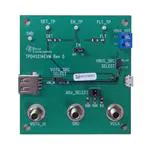
TPD4S214EVM
1
Introduction
The TPD4S214 is a single-chip protection solution for USB On-the-Go and other current limited USB
applications. This device includes an integrated low RDS(ON) N-channel current limited switch for OTG
current supply to peripheral devices. TPD4S214 offers low capacitance TVS ESD clamps for the D+, D–,
and ID pins for both USB2.0 and USB3.0 applications. The VBUS pin can handle continuous voltage
ranging from –2V to 30V. The over voltage lock-out (OVLO) at the VBUS pin ensures that if there is a fault
condition at the VBUS line, the TPD4S214 is able to isolate it and protects the system from damage.
Similarly, the under voltage lock out (UVLO) at the VOTG_IN pin ensures that there is no power drain
from the internal OTG supply to external VBUS if VOTG_IN drops below safe operating level.
When EN is high, the OTG switch is activated and the FLT pin indicates whether there is a fault condition.
The soft start feature waits 16 ms to turn on the OTG switch after all operating conditions are met. The
FLT pin asserts low during any one of the following fault conditions: OVLO (VBUS > VOVLO), over
temperature, over current, short circuit condition, or reverse-current-condition (VBUS > VOTG_IN). The OTG
switch is turned off during any fault condition; in addition, it is also turned off during UVLO condition
(VOTG_IN < VUVLO). Once the switch is turned off, the IC periodically rechecks the faults and UVLO internally.
If the IC returns to normal operating conditions, the switch turns back on and FLT is reset to high.
There is also a VBUS detection feature for facilitating USB communication between USB host and
peripheral device. Refer to Table 2 in data sheet for detection scheme. If this is not used, DET pin can be
either floating or connected to ground.
SLVU839 – February 2013
Submit Documentation Feedback
TPD4S214EVM
Copyright © 2013, Texas Instruments Incorporated
1
�Highlighted Features
2
www.ti.com
Highlighted Features
•
•
•
•
•
•
•
•
•
•
•
•
•
•
Input Voltage Protection at VBUS up to 30V
Low RDS(ON) N-CH FET Switch for high efficiency
Compliant with USB2.0 and USB3.0 OTG spec
User Adjustable current limit from 250mA to beyond 900mA
Built-in soft-start
Reverse current blocking
Over Voltage Lock Out for VBUS
Under Voltage Lock Out for VOTG_IN
Thermal shutdown and short circuit protection
Auto retry on any fault; no latching off states
Integrated VBUS detection circuit
Low Capacitance TVS ESD Clamp for USB2.0 High speed Data Rate
Internal 16ms startup delay
ESD Performance D+/D–/ID/VBUS Pins:
– ±15-kV Contact Discharge (IEC 61000-4-2)
– ±15-kV Air Gap Discharge (IEC 61000-4-2)
Space Saving WCSP (12-YFF) Package
3
EVM Description
The TPD4S214EVM provides full functionality of TPD4S214. Dependent on the jumper configurations,
VOTG_IN can be supplied through either the USB Type-A connector labeled USB_IN or the banana jack
labeled VOTG_IN. VBUS can be output to either the Micro USB-B connector labeled USB_OUT or a two
pin terminal block labeled VBUS_OUT. This configuration allows the device to be tested without the use of
expensive breakout boards; yet one or two breakout boards can still be accommodated. D+/D– lines can
only be characterized through the USB connectors.
Test points are provided for monitoring the DET, EN, and FLT logic pins.
VBUS current limiting adjustments are made by jumper selection of ADJ_SEL. R3 is left unpopulated to
allow for a custom user preferred value.
2
TPD4S214EVM
SLVU839 – February 2013
Submit Documentation Feedback
Copyright © 2013, Texas Instruments Incorporated
�EVM Description
www.ti.com
Table 1. Jumper Configurations
Jumper Configurations
VOTG_IN Source selection
USB_IN port
VOTG_IN banana connector
EN
Sets EN pin low
Sets EN pin high in reference to VCCA
Table 2. Jumper Configurations
VBUS_OUT
VBUS_OUT
USB_OUT
USB_OUT
Jumper Configurations
VBUS Source selection
VBUS_OUT Terminal block
USB_OUT connector
Table 3. Jumper Configurations
VBUS current limiter
adjust
56K
ADJ_SELECT
110K
~ 1A
R3
56K
110K
R3
~ 0.5A
SLVU839 – February 2013
Submit Documentation Feedback
56K
110K
~ 1.5A
R3
56K
110K
R3
User supplied
TPD4S214EVM
Copyright © 2013, Texas Instruments Incorporated
3
�Bill of Materials
4
www.ti.com
Bill of Materials
Table 4. Bill of Materials
Qty
4
RefDes
Size
1
U1
0.051 inch x 0.067
1
CBUS
603
1
COTG
603
3
J4 J6 J8
1
Value
Description
Part Number
MFR
IC, USB OTG COMPANION DEVICE
TPD4S214YFF
TI
1uF
Capacitor, Ceramic Chip, 10V, ±10%
STD
STD
10uF
Capacitor, Ceramic Chip, 10V, ±10%
STD
STD
0.300 inch dia
Connector, Banana Jack, Uninsulated
3267
Pomona
J5
0.354 inch x 0.628
Connector,15A, 300V Male 2 Pole, 5.08 mm
ED120/2DS
On Shore Technology Inc.
1
USB_OUT
0.201 inch x 0.295
Connector, SMT, Micro USB-B, flangeless
SD-105017-1001
Molex
1
USB_IN
0.596 inch x 0.618
CONN USB 2.0 R/A FMAL TYPE-A SMD
AU-Y1006-2-R
Assman WSW Components
2
D1-2
603
SML-LX0603GW-TR
Diode, LED, Red, 1.8, 2mA, 2.5 mcd
SML-311UTT86
Rohm Semiconductor
3
J1-3
0.10 inch x 0.30
PEC03SAAN
Header, Male 3-pin, 100mil spacing,
PEC03SAAN
Sullins
1
J7
0.20 inch x 0.30
PEC03DAAN
Header, Male 2x3-pin, 100mil spacing
PEC03DAAN
Sullins
2
R4-5
1206
10K
Resistor, Metal Film, 1/4 watt, ±5%
STD
STD
1
R2
1206
110K
Resistor, Metal Film, 1/4 watt, ±5%
STD
STD
1
R1
1206
56K
Resistor, Metal Film, 1/4 watt, ±5%
STD
STD
4
TP1-4
0.100 inch dia.
5002
Test Point, White, Thru Hole Color Keyed
5002K-ND
Keystone
TPD4S214EVM
SLVU839 – February 2013
Submit Documentation Feedback
Copyright © 2013, Texas Instruments Incorporated
�Schematic
www.ti.com
5
Schematic
Figure 1. Schematic Drawing
SLVU839 – February 2013
Submit Documentation Feedback
TPD4S214EVM
Copyright © 2013, Texas Instruments Incorporated
5
�IMPORTANT NOTICE
Texas Instruments Incorporated and its subsidiaries (TI) reserve the right to make corrections, enhancements, improvements and other
changes to its semiconductor products and services per JESD46, latest issue, and to discontinue any product or service per JESD48, latest
issue. Buyers should obtain the latest relevant information before placing orders and should verify that such information is current and
complete. All semiconductor products (also referred to herein as “components”) are sold subject to TI’s terms and conditions of sale
supplied at the time of order acknowledgment.
TI warrants performance of its components to the specifications applicable at the time of sale, in accordance with the warranty in TI’s terms
and conditions of sale of semiconductor products. Testing and other quality control techniques are used to the extent TI deems necessary
to support this warranty. Except where mandated by applicable law, testing of all parameters of each component is not necessarily
performed.
TI assumes no liability for applications assistance or the design of Buyers’ products. Buyers are responsible for their products and
applications using TI components. To minimize the risks associated with Buyers’ products and applications, Buyers should provide
adequate design and operating safeguards.
TI does not warrant or represent that any license, either express or implied, is granted under any patent right, copyright, mask work right, or
other intellectual property right relating to any combination, machine, or process in which TI components or services are used. Information
published by TI regarding third-party products or services does not constitute a license to use such products or services or a warranty or
endorsement thereof. Use of such information may require a license from a third party under the patents or other intellectual property of the
third party, or a license from TI under the patents or other intellectual property of TI.
Reproduction of significant portions of TI information in TI data books or data sheets is permissible only if reproduction is without alteration
and is accompanied by all associated warranties, conditions, limitations, and notices. TI is not responsible or liable for such altered
documentation. Information of third parties may be subject to additional restrictions.
Resale of TI components or services with statements different from or beyond the parameters stated by TI for that component or service
voids all express and any implied warranties for the associated TI component or service and is an unfair and deceptive business practice.
TI is not responsible or liable for any such statements.
Buyer acknowledges and agrees that it is solely responsible for compliance with all legal, regulatory and safety-related requirements
concerning its products, and any use of TI components in its applications, notwithstanding any applications-related information or support
that may be provided by TI. Buyer represents and agrees that it has all the necessary expertise to create and implement safeguards which
anticipate dangerous consequences of failures, monitor failures and their consequences, lessen the likelihood of failures that might cause
harm and take appropriate remedial actions. Buyer will fully indemnify TI and its representatives against any damages arising out of the use
of any TI components in safety-critical applications.
In some cases, TI components may be promoted specifically to facilitate safety-related applications. With such components, TI’s goal is to
help enable customers to design and create their own end-product solutions that meet applicable functional safety standards and
requirements. Nonetheless, such components are subject to these terms.
No TI components are authorized for use in FDA Class III (or similar life-critical medical equipment) unless authorized officers of the parties
have executed a special agreement specifically governing such use.
Only those TI components which TI has specifically designated as military grade or “enhanced plastic” are designed and intended for use in
military/aerospace applications or environments. Buyer acknowledges and agrees that any military or aerospace use of TI components
which have not been so designated is solely at the Buyer's risk, and that Buyer is solely responsible for compliance with all legal and
regulatory requirements in connection with such use.
TI has specifically designated certain components as meeting ISO/TS16949 requirements, mainly for automotive use. In any case of use of
non-designated products, TI will not be responsible for any failure to meet ISO/TS16949.
Products
Applications
Audio
www.ti.com/audio
Automotive and Transportation
www.ti.com/automotive
Amplifiers
amplifier.ti.com
Communications and Telecom
www.ti.com/communications
Data Converters
dataconverter.ti.com
Computers and Peripherals
www.ti.com/computers
DLP® Products
www.dlp.com
Consumer Electronics
www.ti.com/consumer-apps
DSP
dsp.ti.com
Energy and Lighting
www.ti.com/energy
Clocks and Timers
www.ti.com/clocks
Industrial
www.ti.com/industrial
Interface
interface.ti.com
Medical
www.ti.com/medical
Logic
logic.ti.com
Security
www.ti.com/security
Power Mgmt
power.ti.com
Space, Avionics and Defense
www.ti.com/space-avionics-defense
Microcontrollers
microcontroller.ti.com
Video and Imaging
www.ti.com/video
RFID
www.ti-rfid.com
OMAP Applications Processors
www.ti.com/omap
TI E2E Community
e2e.ti.com
Wireless Connectivity
www.ti.com/wirelessconnectivity
Mailing Address: Texas Instruments, Post Office Box 655303, Dallas, Texas 75265
Copyright © 2013, Texas Instruments Incorporated
�