���������
�
����
�� ����������� ���
����
SLIS067A − NOVEMBER 1998 − REVISED APRIL 2002
D Dedicated PWM Input Port
D Optimized for Reversible Operation of
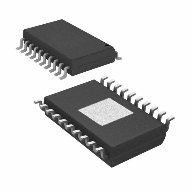
DWP PACKAGE
(TOP VIEW)
Motors
GNDS
VCC
DIR
VCC
OUT1
OUT1
GND
PWM
GND
GNDS
D Two Input Control Lines for Reduced
D
D
D
D
Microcontroller Overhead
Internal Current Shutdown of 5 A
40 V Load Dump Rating
Integrated Fault Protection and Diagnostics
CMOS Compatible Schmitt Trigger Inputs
for High Noise Immunity
description
1
20
2
19
3
18
4
17
5
16
6
15
7
14
8
13
9
12
10
11
GNDS
VCC
STATUS2
VCC
OUT2
OUT2
GND
STATUS1
GND
GNDS
The TPIC0107B is a PWM control intelligent H-bridge designed specifically for dc motor applications. The
device provides forward, reverse, and brake modes of operation. A logic supply voltage of 5 V is internally
derived from VCC.
The TPIC0107B has an extremely low rDS(on), 280 mΩ typical, to minimize system power dissipation. The
direction control (DIR) and PWM control (PWM) inputs greatly simplify the microcontroller overhead
requirement. The PWM input can be driven from a dedicated PWM port while the DIR input is driven as a simple
low speed toggle.
The TPIC0107B provides protection against over-voltage, over-current, over-temperature, and cross
conduction faults. Fault diagnostics can be obtained by monitoring the STATUS1 and STATUS2 terminals and
the two input control lines. STATUS1 is an open-drain output suitable for wired-or connection. STATUS2 is a
push-pull output that provides a latched status output. Under-voltage protection ensures that the outputs, OUT1
and OUT2, will be disabled when VCC is less than the under-voltage detection voltage V(UVCC).
The TPIC0107B is designed using TI’s LinBiCMOS process. LinBiCMOS allows the integration of low power
CMOS structures, precision bipolar cells, and low impedance DMOS transistors.
The TPIC0107B is offered in a 20-pin thermally enhanced small-outline package (DWP) and is characterized
for operation over the operating case temperature of −40°C to 125°C.
FUNCTION TABLE
DIR
PWM
OUT1
OUT2
0
0
HS
HS
Brake, both HSDs turned on hard
0
1
HS
LS
Motor turns counter clockwise
1
0
HS
HS
Brake, both HSDs turned on hard
1
1
LS
HS
Motor turns clockwise
MODE
Please be aware that an important notice concerning availability, standard warranty, and use in critical applications of
Texas Instruments semiconductor products and disclaimers thereto appears at the end of this data sheet.
LinBiCMOS is a trademark of Texas Instruments Incorporated.
Copyright 2002, Texas Instruments Incorporated
�
�������� ���� ����������� �� �!��"�� �� �� #!$%������� &��"'
���&!��� ������� �� �#"����������� #"� �(" �"��� �� �")�� �����!�"���
����&��& *������+' ���&!����� #���"����, &�"� ��� �"�"�����%+ ���%!&"
�"����, �� �%% #����"�"��'
POST OFFICE BOX 655303
• DALLAS, TEXAS 75265
1
����������
�
����
�� ����������� ���
����
SLIS067A − NOVEMBER 1998 − REVISED APRIL 2002
block diagram
VCC
OverCurrent
Protection
HSD
PWM
OverVoltage
Detection
Logic
DIR
STATUS1
STATUS2
DMOS
Driver
5V
Reg.
Charge
Pump
(2 MHz)
UnderVoltage
Detection
DMOS
Driver
OUT2
OUT1
OpenCircuit
Detect
OverTemperature
Detection
Load-Dump
Protection
DMOS
Driver
DMOS
Driver
OverCurrent
Protection
LSD
GND
Terminal Functions
TERMINAL
NAME
NO.
I/O
DESCRIPTION
DIR
3
I
Direction control input
GND
7, 9,
12, 14
I
Power ground
GNDS
1, 10,
11, 20
I
Substrate ground
OUT1
5, 6
O
Half-H output. DMOS output
OUT2
15, 16
O
Half-H output. DMOS output
PWM
8
I
PWM control input
STATUS1
13
O
Status output
STATUS2
18
O
Latched status output
2, 4,
17, 19
I
Supply voltage
VCC
NOTE: It is mandatory that all four ground terminals plus at least one substrate terminal are connected to the system ground. Use all VCC and
OUT terminals.
2
POST OFFICE BOX 655303
• DALLAS, TEXAS 75265
����������
�
����
�� ����������� ���
����
SLIS067A − NOVEMBER 1998 − REVISED APRIL 2002
schematics of inputs and outputs
STATUS1
STATUS2
DIR/PWM
absolute maximum ratings over operating case temperature range (unless otherwise noted)†
Power supply voltage range, VCC . . . . . . . . . . . . . . . . . . . . . . . . . . . . . . . . . . . . . . . . . . . . . . . . . . . −0.3 V to 33 V
Logic input voltage range, VIN . . . . . . . . . . . . . . . . . . . . . . . . . . . . . . . . . . . . . . . . . . . . . . . . . . . . . . . −0.3 V to 7 V
Load dump (for 400 ms, TC = 25°C) . . . . . . . . . . . . . . . . . . . . . . . . . . . . . . . . . . . . . . . . . . . . . . . . . . . . . . . . . . 40 V
Status output voltage range, VO(status) . . . . . . . . . . . . . . . . . . . . . . . . . . . . . . . . . . . . . . . . . . . . . . . −0.3 V to 7 V
Continuous power dissipation, TC = 25°C . . . . . . . . . . . . . . . . . . . . . . . . . . . . . . . . . . . . . . . . . . . . . . . . . . . 1.29 W
Storage temperature range, Tstg . . . . . . . . . . . . . . . . . . . . . . . . . . . . . . . . . . . . . . . . . . . . . . . . . . . −55°C to 150°C
Maximum junction temperature, TJ . . . . . . . . . . . . . . . . . . . . . . . . . . . . . . . . . . . . . . . . . . . . . . . . . . . . . . . . . 150°C
† Stresses beyond those listed under “absolute maximum ratings” may cause permanent damage to the device. These are stress ratings only, and
functional operation of the device at these or any other conditions beyond those indicated under “recommended operating conditions” is not
implied. Exposure to absolute-maximum-rated conditions for extended periods may affect device reliability.
DISSIPATION RATING TABLE
TA ≤ 25°C
POWER RATING
DERATING FACTOR
ABOVE TA = 25°C
TA = 70°C
POWER RATING
TA = 125°C
POWER RATING
1.29 W
0.0104 W/°C
0.82 W
0.25 W
recommended operating conditions
MIN
Supply voltage, VCC
Operating case temperature, TC
Switching frequency, fPWM
POST OFFICE BOX 655303
• DALLAS, TEXAS 75265
MAX
UNIT
6
18
V
−40
125
°C
2
kHz
3
����������
�
����
�� ����������� ���
����
SLIS067A − NOVEMBER 1998 − REVISED APRIL 2002
electrical characteristics over recommended operating case temperature range and VCC = 5 V to
6 V (unless otherwise noted)
PARAMETER
rDS(on)
TEST CONDITIONS
Static drain-source on-resistance (per transistor)
I(BR) = 1 A
MIN
TYP
MAX
TJ = 25°C
TJ = 150°C
550
LSD
TJ = 25°C
TJ = 150°C
600
HSD
850
870
Under voltage detection on VCC, switch off voltage
See Note 1
5
V
V(UVCC(ON))
V(STL)
Under voltage detection on VCC, switch on voltage
See Note 1
5.2
V
STATUS low output voltage
0.8
V
V(ST2H)
I(ST(OFF))
STATUS2 high output voltage
IO = 100 µA, See Note 1
IO = 20 µA, See Note 1
STATUS output leakage current
V(ST) = 5 V, See Note 1
VIL
VIH
Low level logic input voltage
High level logic input voltage
∆VI
IIH
Hysteresis of input voltage
0.3
3
100
mΩ
Open circuit detection current
VIH = 3.5 V
40
mΩ
I(QCD)
V(UVCC(OFF))
High level logic input current
10
UNIT
mA
5.4
V
5
µA
−0.3
0.5
V
3.6
7
V
2
V
10
50
µA
NOTE 1: The device functions according to the function table for VCC between V(UVCC) and 5 V (no parameters specified). STATUS outputs are
not defined for VCC less than V(UVCC).
4
POST OFFICE BOX 655303
• DALLAS, TEXAS 75265
����������
�
����
�� ����������� ���
����
SLIS067A − NOVEMBER 1998 − REVISED APRIL 2002
electrical characteristics over recommended operating case temperature and supply voltage
ranges (unless otherwise noted) (see Note 2)
PARAMETER
TEST CONDITIONS
Static drain-source on-resistance
(per transistor) IBR = 1 A
TYP
TJ = 25°C
TJ = 150°C
VCC = 6 V to 9 V
VCC = 9 V to 18 V
400
TJ = 25°C
VCC = 6 V to 9 V
VCC = 9 V to 18 V
280
TJ = 150°C
VCC = 6 V to 9 V
VCC = 9 V to 18 V
LSD
rDS(on)
MIN
VCC = 6 V to 9 V
VCC = 9 V to 18 V
HSD
MAX
280
340
620
430
340
640
10
400
560
40
100
Open circuit detection current
Static thermal shutdown temperature
See Notes 3 and 4
140
TSDD
Dynamic thermal shutdown temperature
See Notes 3 and 5
160
4.8
7.5
ICS
Current shutdown limit
VCC = 6 V to 9 V
VCC = 9 V to 18 V
5
7.5
I(CON)
Continuous bridge current
TJ = 125°C, Operating lifetime 10,000 hours,
(see Figure 1)
V(OVCC)
V(STL)
Over voltage detection on VCC
V(ST2H)
I(ST(OFF))
STATUS2 high output voltage
IO = 100 µA
IO = 20 µA
STATUS output leakage current
V(ST) = 5 V
VIL
VIH
Low level logic input voltage
High level logic input voltage
∆VI
IIH
Hysteresis of input voltage
0.3
mA
°C
3.9
VIH = 3.5 V
mΩ
°C
27
High level logic input current
mΩ
560
I(QCD)
TSDS
STATUS low output voltage
UNIT
380
A
3
A
36
V
0.8
V
5.4
V
5
µA
−0.3
0.8
V
3.6
7
V
2
V
10
50
µA
NOTES: 2. The device functions according to the function table for VCC between 18 V and V(OVCC), but only up to a maximum supply voltage
of 33 V (no parameters specified). Exposure beyond 18 V for extended periods may affect device reliability.
3. Exposure beyond absolute-maximum-rated condition of junction temperature may affect device reliability.
4. No temperature gradient between DMOS transistor and temperature sensor.
5. With temperature gradient between DMOS transistor and temperature sensor in a typical application (DMOS transistor as heat
source).
switching characteristics over recommended operating case temperature and supply voltage
ranges (unless otherwise noted)
PARAMETER
TEST CONDITIONS
MIN
TYP
High-side driver turn-on time
tout(on)
100
Low-side driver turn-on time
VDS(on)20,000 h
3A
125°C
>10,000 h
POST OFFICE BOX 655303
• DALLAS, TEXAS 75265
����������
�
����
�� ����������� ���
����
SLIS067A − NOVEMBER 1998 − REVISED APRIL 2002
PARAMETER MEASUREMENT INFORMATION
operating wave forms
DIR (Low)
PWM
STATUS1
STATUS2
OUT1 (High)
OUT2
Open Circuit
10 mA (min.) for a period
>1 ms (min.), the fault flags are set. However, the output transistors will not be disabled.
† All limits mentioned are typical values unless otherwise noted.
‡ If a short circuit occurs (i.e., the over-current detection circuitry is activated) at a supply voltage higher than 16.5 V and a junction temperature
higher than 90°C, damage to the device may occur.
POST OFFICE BOX 655303
• DALLAS, TEXAS 75265
9
����������
�
����
�� ����������� ���
����
SLIS067A − NOVEMBER 1998 − REVISED APRIL 2002
PRINCIPLES OF OPERATION
DIAGNOSTICS TABLE (see Note 6)
DIR
PWM
OUT1
OUT2
STATUS1†
STATUS2
Normal operation
0
0
1
1
0
1
0
1
HS
HS
HS
LS
HS
LS
HS
HS
1
1
1
1
1
1
1
1
Open circuit between OUT1 and OUT2
0
0
1
1
0
1
0
1
HS
HS
HS
LS
HS
LS
HS
HS
1
0
1
0
1
0
1
0
Short circuit from OUT1 to OUT2 (see Notes 7 and 8)
0
1
1
1
X
X
X
X
0
0
0
0
Short circuit from OUT1 to GND (see Notes 7 and 8)
0
1
0
0
0
1
X
X
X
X
X
X
0
0
0
0
0
0
Short circuit from OUT2 to GND (see Notes 7 and 8)
0
1
1
0
0
1
X
X
X
X
X
X
0
0
0
0
0
0
Short circuit from OUT1 to VCC (see Notes 7 and 8)
1
1
X
X
0
0
Short circuit from OUT2 to VCC (see Notes 7 and 8)
0
1
X
X
0
0
Over temperature
0
0
1
1
0
1
0
1
Z
Z
Z
Z
Z
Z
Z
Z
0
0
0
0
0
0
0
0
FLAG
† When wired with a pull-up resistor
SYMBOL
VALUE
0
Logic low
1
Logic high
HS
High-side MOSFET conducting
LS
Low-side MOSFET conducting
Z
No output transistors conducting
X
Voltage level undefined
NOTES: 6. All input combinations not stated result in STATUS output = 1.
7. STATUS1 active for a minimum of 3 µs.
8. STATUS2 active until an input is toggled.
10
POST OFFICE BOX 655303
• DALLAS, TEXAS 75265
����������
�
����
�� ����������� ���
����
SLIS067A − NOVEMBER 1998 − REVISED APRIL 2002
TYPICAL CHARACTERISTICS
VCC = 9.18 V
300
200
100
0
−40 −20
0
20
40
60
80
100
120 140
r DS(on) − Static Drain-Source On-Resistance − m Ω
STATIC-DRAIN-SOURCE ON-RESISTANCE
vs
SUPPLY VOLTAGE
400
600
HSD, TJ = 125°C
500
LSD, TJ = 125°C
400
300
HSD, TJ = 25°C
LSD, TJ = 25°C
200
100
0
0
5
TJ − Junction Temperature − °C
10
15
20
25
VCC − Supply Voltage − V
Figure 6
Figure 7
OUTPUT STAGE TURN-ON TIME
vs
JUNCTION TEMPERATURE
20
t out(on) − Output Stage Turn-On Time − µ s
r DS(on) − Static Drain-Source On-Resistance − m Ω
STATIC DRAIN-SOURCE ON-RESISTANCE
vs
JUNCTION TEMPERATURE
15
HSD, VCC = 13.2 V
10
LSD, VCC = 13.2 V
5
0
−40 −20
0
20
40
60 80 100
TJ − Junction Temperature − °C
120 140
Figure 8
POST OFFICE BOX 655303
• DALLAS, TEXAS 75265
11
����������
�
����
�� ����������� ���
����
SLIS067A − NOVEMBER 1998 − REVISED APRIL 2002
APPLICATION INFORMATION
5V
VCC
100 kΩ
VCC
DIR
PWM
OUT1
TPIC0107B
STATUS1
M
100 nF
47 µF†
OUT2
STATUS2
GND GNDS
CONTROL DIAGNOSTIC
Microcontroller
† Necessary for isolating supply voltage or interruption (e.g., 47 µF).
NOTE: If a STATUS output is not connected to the appropriate microcontroller input, it shall remain unconnected.
12
POST OFFICE BOX 655303
• DALLAS, TEXAS 75265
�PACKAGE OPTION ADDENDUM
www.ti.com
11-Dec-2008
PACKAGING INFORMATION
Orderable Device
Status (1)
Package
Type
Package
Drawing
Pins Package Eco Plan (2)
Qty
TPIC0107BDWP
OBSOLETE
SO
Power
PAD
DWP
20
TBD
Call TI
Call TI
TPIC0107BDWPG4
OBSOLETE
SO
Power
PAD
DWP
20
TBD
Call TI
Call TI
TPIC0107BDWPRG4
OBSOLETE
SO
Power
PAD
DWP
20
TBD
Call TI
Call TI
Lead/Ball Finish
MSL Peak Temp (3)
(1)
The marketing status values are defined as follows:
ACTIVE: Product device recommended for new designs.
LIFEBUY: TI has announced that the device will be discontinued, and a lifetime-buy period is in effect.
NRND: Not recommended for new designs. Device is in production to support existing customers, but TI does not recommend using this part in
a new design.
PREVIEW: Device has been announced but is not in production. Samples may or may not be available.
OBSOLETE: TI has discontinued the production of the device.
(2)
Eco Plan - The planned eco-friendly classification: Pb-Free (RoHS), Pb-Free (RoHS Exempt), or Green (RoHS & no Sb/Br) - please check
http://www.ti.com/productcontent for the latest availability information and additional product content details.
TBD: The Pb-Free/Green conversion plan has not been defined.
Pb-Free (RoHS): TI's terms "Lead-Free" or "Pb-Free" mean semiconductor products that are compatible with the current RoHS requirements
for all 6 substances, including the requirement that lead not exceed 0.1% by weight in homogeneous materials. Where designed to be soldered
at high temperatures, TI Pb-Free products are suitable for use in specified lead-free processes.
Pb-Free (RoHS Exempt): This component has a RoHS exemption for either 1) lead-based flip-chip solder bumps used between the die and
package, or 2) lead-based die adhesive used between the die and leadframe. The component is otherwise considered Pb-Free (RoHS
compatible) as defined above.
Green (RoHS & no Sb/Br): TI defines "Green" to mean Pb-Free (RoHS compatible), and free of Bromine (Br) and Antimony (Sb) based flame
retardants (Br or Sb do not exceed 0.1% by weight in homogeneous material)
(3)
MSL, Peak Temp. -- The Moisture Sensitivity Level rating according to the JEDEC industry standard classifications, and peak solder
temperature.
Important Information and Disclaimer:The information provided on this page represents TI's knowledge and belief as of the date that it is
provided. TI bases its knowledge and belief on information provided by third parties, and makes no representation or warranty as to the
accuracy of such information. Efforts are underway to better integrate information from third parties. TI has taken and continues to take
reasonable steps to provide representative and accurate information but may not have conducted destructive testing or chemical analysis on
incoming materials and chemicals. TI and TI suppliers consider certain information to be proprietary, and thus CAS numbers and other limited
information may not be available for release.
In no event shall TI's liability arising out of such information exceed the total purchase price of the TI part(s) at issue in this document sold by TI
to Customer on an annual basis.
Addendum-Page 1
��IMPORTANT NOTICE
Texas Instruments Incorporated and its subsidiaries (TI) reserve the right to make corrections, modifications, enhancements, improvements,
and other changes to its products and services at any time and to discontinue any product or service without notice. Customers should
obtain the latest relevant information before placing orders and should verify that such information is current and complete. All products are
sold subject to TI’s terms and conditions of sale supplied at the time of order acknowledgment.
TI warrants performance of its hardware products to the specifications applicable at the time of sale in accordance with TI’s standard
warranty. Testing and other quality control techniques are used to the extent TI deems necessary to support this warranty. Except where
mandated by government requirements, testing of all parameters of each product is not necessarily performed.
TI assumes no liability for applications assistance or customer product design. Customers are responsible for their products and
applications using TI components. To minimize the risks associated with customer products and applications, customers should provide
adequate design and operating safeguards.
TI does not warrant or represent that any license, either express or implied, is granted under any TI patent right, copyright, mask work right,
or other TI intellectual property right relating to any combination, machine, or process in which TI products or services are used. Information
published by TI regarding third-party products or services does not constitute a license from TI to use such products or services or a
warranty or endorsement thereof. Use of such information may require a license from a third party under the patents or other intellectual
property of the third party, or a license from TI under the patents or other intellectual property of TI.
Reproduction of TI information in TI data books or data sheets is permissible only if reproduction is without alteration and is accompanied
by all associated warranties, conditions, limitations, and notices. Reproduction of this information with alteration is an unfair and deceptive
business practice. TI is not responsible or liable for such altered documentation. Information of third parties may be subject to additional
restrictions.
Resale of TI products or services with statements different from or beyond the parameters stated by TI for that product or service voids all
express and any implied warranties for the associated TI product or service and is an unfair and deceptive business practice. TI is not
responsible or liable for any such statements.
TI products are not authorized for use in safety-critical applications (such as life support) where a failure of the TI product would reasonably
be expected to cause severe personal injury or death, unless officers of the parties have executed an agreement specifically governing
such use. Buyers represent that they have all necessary expertise in the safety and regulatory ramifications of their applications, and
acknowledge and agree that they are solely responsible for all legal, regulatory and safety-related requirements concerning their products
and any use of TI products in such safety-critical applications, notwithstanding any applications-related information or support that may be
provided by TI. Further, Buyers must fully indemnify TI and its representatives against any damages arising out of the use of TI products in
such safety-critical applications.
TI products are neither designed nor intended for use in military/aerospace applications or environments unless the TI products are
specifically designated by TI as military-grade or "enhanced plastic." Only products designated by TI as military-grade meet military
specifications. Buyers acknowledge and agree that any such use of TI products which TI has not designated as military-grade is solely at
the Buyer's risk, and that they are solely responsible for compliance with all legal and regulatory requirements in connection with such use.
TI products are neither designed nor intended for use in automotive applications or environments unless the specific TI products are
designated by TI as compliant with ISO/TS 16949 requirements. Buyers acknowledge and agree that, if they use any non-designated
products in automotive applications, TI will not be responsible for any failure to meet such requirements.
Following are URLs where you can obtain information on other Texas Instruments products and application solutions:
Products
Applications
Amplifiers
amplifier.ti.com
Audio
www.ti.com/audio
Data Converters
dataconverter.ti.com
Automotive
www.ti.com/automotive
DLP® Products
www.dlp.com
Communications and
Telecom
www.ti.com/communications
DSP
dsp.ti.com
Computers and
Peripherals
www.ti.com/computers
Clocks and Timers
www.ti.com/clocks
Consumer Electronics
www.ti.com/consumer-apps
Interface
interface.ti.com
Energy
www.ti.com/energy
Logic
logic.ti.com
Industrial
www.ti.com/industrial
Power Mgmt
power.ti.com
Medical
www.ti.com/medical
Microcontrollers
microcontroller.ti.com
Security
www.ti.com/security
RFID
www.ti-rfid.com
Space, Avionics &
Defense
www.ti.com/space-avionics-defense
RF/IF and ZigBee® Solutions www.ti.com/lprf
Video and Imaging
www.ti.com/video
Wireless
www.ti.com/wireless-apps
Mailing Address: Texas Instruments, Post Office Box 655303, Dallas, Texas 75265
Copyright © 2010, Texas Instruments Incorporated
�


 工商网监
湘ICP备2023018690号
工商网监
湘ICP备2023018690号
