Product
Folder
Sample &
Buy
Support &
Community
Tools &
Software
Technical
Documents
TPIC2040
SLIS172 – DECEMBER 2015
TPIC2040 Serial I/F Controlled 7-Channel Motor-Driver for ODD Drive
1 Features
•
•
•
•
•
•
Serial Peripheral Interface (SPI)
– Maximum Read/Write 35 MHz
– 3.3-V Digital I/O
Actuator and Motor Driver
– PWM Control With H-Bridge Output
– Focus / Tracking / Tilt Actuator Driver With 12Bit DAC Control
– Sled Motor Drivers With Current Mode, 10-Bit
DAC Control
– Load Driver With 12-Bit DAC Control
– Capable End Position Sensing for Sled
Without Position Sensor
Spindle Motor Driver
– Integrated Spindle Current Sense Resistor
– Selectable Current Sense Resistor Value 0.27
to 0.20 Ω by Register Setting; Thereby, SPM
Current can be Restricted from 725 to 980 mA
– Sensor-Less: Rotor Position Sense by Motor
BEMF
– 12-Bit Spindle DAC Programmed Through
Serial Port
– Self-Contained Inductive Position Sense and
Startup
– Quick Stop by Automatic Controlled Brake
Named Auto Short Brake (Short and Active
Brake)
– 0.7-A Maximum Continuous Current Excluding
Thermal Issues
– LS Mode: Restricted to 25% of Normal Speed
Utility Functions
– XRESET Signal With Digital Delay (POR) 20
ms
– Status Latch: Act Timer, SIF Error, PWR
Monitor, Thermal Protection, and OCP Error
Switch
– CSW: Software Control Current Output Port
LDO Pre-Driver
– 1-Channel LDO Pre-Driver for 3.3-V or 1.2-V
Output With External Transistor
Protection
– Individual Thermal Protect Circuit on CSW,
SPM, and Act Channel
– Two Alert Levels: Pre-Detect and Detect in
Thermal Protection
– Overcurrent Protection Circuit in Load Driver
2 Applications
•
•
•
DVD Player
CD Player
Optical Disk Drive
3 Description
TPIC2040 is a very-low noise type motor driver IC
suitable for slim or ultra-slim DVD reader/writer. This
IC includes integrated current sense resistance that
measures SPM current and reduces drive system
cost. The 7-channel driver IC controlled by serial I/F
is optimum for driving a spindle motor, a sled motor,
a load motor, and Focus / Tracking / Tilt actuators.
The spindle motor driver uses BEMF detection for
sensorless startup and control of the spindle motor
Device Information(1)
PART NUMBER
TPIC2040DBT
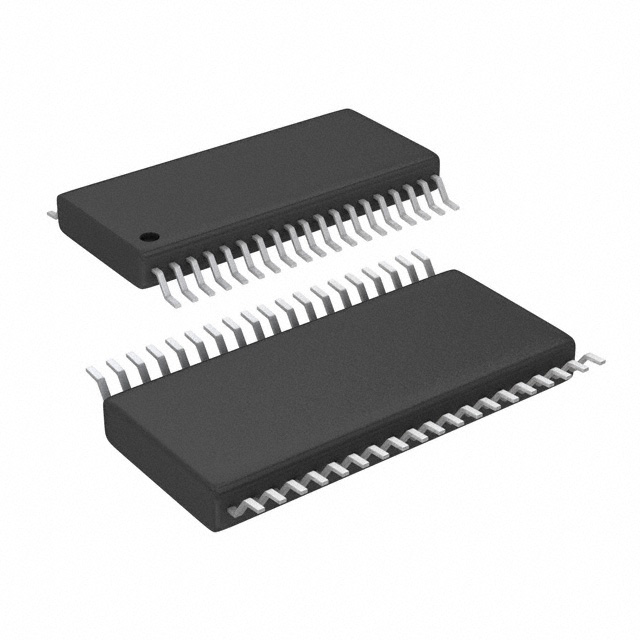
PACKAGE
BODY SIZE (NOM)
TSSOP (38)
9.70 mm × 4.40 mm
(1) For all available packages, see the orderable addendum at
the end of the data sheet.
Simplified Block Diagram
MCOM
TPIC2040
5V
5V
SPM
Driver
3.3 V
U
V
W
SLED1+
Controller
•
1
– Selectable OCP Threshold Level in CSW
Output
– Hardware Device Disable Pin XMUTE
– Power Monitor by Undervoltage Lockout
(UVLO) and Overvoltage Protection (OVP)
5V
SLED1
SPI
SLED1SLED2+
5V
SLED2
1PX V
output
5V
TLT
5V
LIN9VG
LDO
Control
9Vout
5V
FCS
SLED2TLT+
TLTFCS+
FCSTRK+
LINFB
5V
TRK
TRKLOAD+
5V
LOAD
LOAD-
1
An IMPORTANT NOTICE at the end of this data sheet addresses availability, warranty, changes, use in safety-critical applications,
intellectual property matters and other important disclaimers. PRODUCTION DATA.
�TPIC2040
SLIS172 – DECEMBER 2015
www.ti.com
Table of Contents
1
2
3
4
5
6
7
Features ..................................................................
Applications ...........................................................
Description .............................................................
Revision History.....................................................
Description (continued).........................................
Pin Configuration and Functions .........................
Specifications.........................................................
7.16 Serial I/F Read Timing Requirements................... 10
7.17 Typical Characteristics .......................................... 11
1
1
1
2
3
3
5
8
Detailed Description ............................................ 12
8.1
8.2
8.3
8.4
8.5
8.6
7.1
7.2
7.3
7.4
7.5
7.6
7.7
7.8
Absolute Maximum Ratings ...................................... 5
ESD Ratings.............................................................. 5
Recommended Operating Conditions....................... 6
Thermal Information .................................................. 6
Electrical Characteristics – Common Part ................ 7
Electrical Characteristics – Charge Pump ................ 7
Electrical Characteristics – LDO Pre Driver Part ...... 8
Electrical Characteristics – Spindle Motor Driver
Part............................................................................. 8
7.9 Electrical Characteristics – Sled Motor Driver Part... 8
7.10 Electrical Characteristics – Focus/
Tilt/Tracking/Driver Part ............................................. 9
7.11 Electrical Characteristics – Load Driver Part .......... 9
7.12 Electrical Characteristics – Current Switch Part ..... 9
7.13 Electrical Characteristics – Actuator Protection ...... 9
7.14 Electrical Characteristics – Serial Port Voltage
Levels ...................................................................... 10
7.15 Serial Port I/F Write Timing Requirements ........... 10
9
Overview .................................................................
Functional Block Diagram .......................................
Feature Description.................................................
Device Functional Modes........................................
Programming ..........................................................
Register Maps .........................................................
12
13
14
19
21
23
Application and Implementation ........................ 39
9.1 Application Information............................................ 39
9.2 Typical Application ................................................. 48
10 Power Supply Recommendations ..................... 50
11 Layout................................................................... 50
11.1 Layout Guidelines ................................................. 50
11.2 Layout Example .................................................... 50
12 Device and Documentation Support ................. 51
12.1
12.2
12.3
12.4
12.5
Device Support ....................................................
Community Resources..........................................
Trademarks ...........................................................
Electrostatic Discharge Caution ............................
Glossary ................................................................
51
51
51
51
51
13 Mechanical, Packaging, and Orderable
Information ........................................................... 51
4 Revision History
2
DATE
REVISION
NOTES
December 2015
*
Initial release.
Submit Documentation Feedback
Copyright © 2015, Texas Instruments Incorporated
Product Folder Links: TPIC2040
�TPIC2040
www.ti.com
SLIS172 – DECEMBER 2015
5 Description (continued)
As the output stage of all channels works in efficient PWM driving, it is possible to attain low-power operation by
PWM control. Deadband less control is possible for a focus / tracking / tilt actuator driver. In addition, the spindle
part output current limiting circuit, thermal shutdown circuit, sled-end detection circuit, actuator protection and
power-reset circuit are built in.
6 Pin Configuration and Functions
DBT Package
38-Pin TSSOP
Top View
1
LOAD+
SLED2-
38
2
LOAD-
SLED2+
37
3
PGND_1
SLED1-
36
4
SIOV
SLED1+
35
5
SSZ
CSWO
34
6
SCLK
P5V_1
33
7
SIMO
P5V_SPM
32
8
SOMI
W
31
9
XMUTE
U
30
10
XFG
V
29
11
XRESET
PGND_SPM
28
12
CP1
MCOM
27
13
CP2
PGND_2
26
14
CP3
TRK-
25
15
LIN3VG
TRK+
24
16
LINFB/GPOUT
FCS-
23
17
AGND/DGND
FCS+
22
18
CV3P3
TLT-
21
19
P5V_2/A5V
TLT+
20
Pin Functions
PIN
NO.
NAME
I/O
DESCRIPTION
1
LOAD+
O
Load positive output terminal
2
LOAD–
O
Load negative output terminal
3
PGND_1
PS
GND terminal
4
SIOV
PS
Power supply terminal for serial port typical 3.3 V
5
SSZ
I
SIO slave select low active input terminal
6
SCLK
I
SIO serial clock input terminal
7
SIMO
I
SIO slave input master output terminal
8
SOMI
O
SIO slave output master input terminal
Submit Documentation Feedback
Copyright © 2015, Texas Instruments Incorporated
Product Folder Links: TPIC2040
3
�TPIC2040
SLIS172 – DECEMBER 2015
www.ti.com
Pin Functions (continued)
PIN
NO.
4
I/O
NAME
DESCRIPTION
9
XMUTE
IN
XMUTE input terminal to disable driver output
10
XFG
O
Motor speed signal output
11
XRESET
O
Power-on reset output. Internally pulled up to SIOV
12
CP1
MISC
Capacitance connection for charge pump
13
CP2
MISC
Capacitance connection for charge pump
14
CP3
MISC
Capacitance connection for charge pump
15
LIN3VG
O
3.3-V predriver output control signal for external N-channel FET
16
LINFB/GPOUT
I/O
Voltage feedback of 3.3-V predriver (be controlled to LINFB = 1.215 V)
17
AGND/DGND
PS
Ground terminal for internal logic
18
CV3P3
19
P5V_2/A5V
PS
Power supply terminal
20
TLT+
O
Tilt positive output terminal
21
TLT–
O
Tilt negative output terminal
22
FCS+
O
Focus positive output terminal
23
FCS–
O
Focus negative output terminal
24
TRK+
O
Tracking positive output terminal
25
TRK-–
O
Tracking negative output terminal
26
PGND_2
PS
GND terminal
27
MCOM
IN
Motor center tap connection
28
PGND_SPM
PS
GND terminal for spindle driver
29
V
O
V phase output terminal for spindle motor
30
U
O
U phase output terminal for spindle motor
31
W
O
W phase output terminal for spindle motor
32
P5V_SPM
PS
Power supply terminal for spindle driver
33
P5V_1
PS
Power supply terminal
34
CSWO
O
Power switch output for 5-V OEIC in OPU
35
SLED1+
O
Sled1 positive output terminal
36
SLED1–
O
Sled1 negative output terminal
37
SLED2+
O
Sled2 positive output terminal
38
SLED2–
O
Sled2 negative output terminal
MISC
Capacitance terminal for internal 3.3-V regulator
Submit Documentation Feedback
Copyright © 2015, Texas Instruments Incorporated
Product Folder Links: TPIC2040
�TPIC2040
www.ti.com
SLIS172 – DECEMBER 2015
7 Specifications
7.1 Absolute Maximum Ratings
over operating free-air temperature range (unless otherwise noted)
(1)
MIN
+ 5 V supply voltage P5V, P5V_SPM
Spindle output peak voltage
V
7
V
V
Spindle output current
1.0
A
Spindle output peak current (PW ≦ 2 ms, Duty ≦ 30%)
2.5
A
Sled output peak current
0.8
A
Focus/tilt/tracking driver output peak current
1.5
A
0.8
A
–0.3
Load driver output peak current
Power dissipation
(1)
UNIT
6
VCC + 0.3 V
Input/output voltage
Tstg
MAX
See Thermal Information
Operating temperature
–20
75
°C
Storage temperature
–50
150
°C
Stresses beyond those listed under Absolute Maximum Ratings may cause permanent damage to the device. These are stress ratings
only, which do not imply functional operation of the device at these or any other conditions beyond those indicated under Recommended
Operating Conditions. Exposure to absolute-maximum-rated conditions for extended periods may affect device reliability.
7.2 ESD Ratings
VALUE
V(ESD)
(1)
(2)
Electrostatic discharge
Human-body model (HBM), per ANSI/ESDA/JEDEC JS-001 (1)
±2000
Charged-device model (CDM), per JEDEC specification JESD22C101 (2)
±500
UNIT
V
JEDEC document JEP155 states that 500-V HBM allows safe manufacturing with a standard ESD control process.
JEDEC document JEP157 states that 250-V CDM allows safe manufacturing with a standard ESD control process.
Submit Documentation Feedback
Copyright © 2015, Texas Instruments Incorporated
Product Folder Links: TPIC2040
5
�TPIC2040
SLIS172 – DECEMBER 2015
www.ti.com
7.3 Recommended Operating Conditions
over operating free-air temperature range (unless otherwise noted)
MIN
NOM
MAX
UNIT
P5V
Operating supply voltage (apply for P5V)
4.5
5.0
5.5
V
VSIOV
SIOV voltage
3.0
3.3
3.6
V
VSIFH
XMUTE, SIMO, SSZ, SCLK pin H level input voltage range
2.2
SIOV + 0.2
V
VSIFL
XMUTE, SIMO, SSZ, SCLK pin L level input voltage range
–0.2
0.8
V
ISPMOA
Spindle output average current (U, V, W total)
700
mA
ISPMO
Spindle output current
700
mA
ISLDOA
Sled output average current
400
mA
IACTOA
Focus / tracking / tilt / loading output average current
400
mA
ICSWOA
CSWO output average current
500
mA
Fck
SCLK frequency
TO
Operating temperature
30
33.8688
35
MHz
–20
25
75
°C
7.4 Thermal Information
TPIC2040
THERMAL METRIC
(1)
DBT (TSSOP)
UNIT
38 PINS
RθJA
Junction-to-ambient thermal resistance (2)
81.2
°C/W
RθJC(top)
Junction-to-case (top) thermal resistance
27.2
°C/W
RθJB
Junction-to-board thermal resistance
42.3
°C/W
ψJT
Junction-to-top characterization parameter
1.7
°C/W
ψJB
Junction-to-board characterization parameter
41.7
°C/W
RθJC(bot)
Junction-to-case (bottom) thermal resistance
N/A
°C/W
(1)
(2)
6
For more information about traditional and new thermal metrics, see the Semiconductor and IC Package Thermal Metrics application
report, SPRA953.
The JEDEC specification low K (1 s) board design used to derive this data.
Submit Documentation Feedback
Copyright © 2015, Texas Instruments Incorporated
Product Folder Links: TPIC2040
�TPIC2040
www.ti.com
SLIS172 – DECEMBER 2015
7.5 Electrical Characteristics – Common Part
over recommended operating free-air temperature range (P5V ≈ 4.5 to 5.5 V, TA ≈ –20℃ to 75℃, unless otherwise noted)
PARAMETER
TEST CONDITIONS
ISTBY
Stand by supply current
LIN3P3_DIS = 1, XSLEEP = L
VCV3
CV3P3 output voltage
Iload = 25 mA
RXM
XMUTE pulldown resistor
RXRST
XRESET pullup resistor
VXRSTL
XRESET low level output voltage
TPOR
Power-on reset delay
RXFG
XFG output resistor
VXFGH
XFG high-level output voltage
SIOV = 3.3 V, XSLEEP = 1,
IOH = 100 µA
VXFGL
XFG low-level output voltage
SIOV = 3.3 V, XSLEEP = 1,
IOL = –100 µA
RGPO
GPOUT output resistor
VGPOH
GPOUT high-level output voltage
SIOV = 3.3 V, XSLEEP = 1,
GPOUT_ENA = 1,GPOUT_HL = 1,
IOH = 100 µA
VGPOL
GPOUT low-level output voltage
SIOV = 3.3 V, XSLEEP = 1,
GPOUT_ENA = 1, GPOUT_HL = 0,
IOH = 100 µA
tTSD
Thermal protect on temperature
Design specified value
hytTSD
Thermal protect hysteresis
temperature
Vonvcc
Voffvcc
MIN
TYP
MAX
UNIT
2.97
3.3
3.63
V
80
200
320
kΩ
13.2
33
52.8
kΩ
0.3
V
15
20
25
ms
100
200
300
Ω
1.0
SIOV = 3.3 V, IOL = –100 µA
mA
SIOV – 0.3
100
V
200
0.3
V
300
Ω
SIOV – 0.3
V
0.3
V
135
150
165
ºC
5
15
25
ºC
P5V reset on voltage
3.3
3.5
3.7
V
P5V reset off voltage
3.5
3.7
3.9
V
Vhysvcc
P5V reset voltage hysteresis
100
200
300
mV
VonCV3
CV3P3 reset on voltage
2.4
2.5
2.6
V
VoffCV3
CV3P3 reset off voltage
2.5
2.6
2.7
V
VonSIO
SIOV reset on voltage
2.4
2.5
2.6
V
VoffSIO
SIOV reset off voltage
2.5
2.6
2.7
V
VhysSIO
SIOV reset voltage hysteresis
VovpspmOn
OVP detection voltage (spindle)
VovpspmOff
OVP release voltage (spindle)
(1)
(1)
VovpSpmHys OVP voltage hysteresis (spindle)
20
100
140
mV
5.9
6.2
6.4
V
5.7
6.0
6.2
V
(1)
50
200
300
mV
VovpOn
OVP detection voltage
(except spindle) (1)
6.2
6.5
6.7
V
VovpOff
OVP release voltage
(except spindle) (1)
6.0
6.3
6.5
V
VovpHys
OVP voltage hysteresis
(except spindle) (1)
50
200
300
mV
VonLinF
LINFB reset on voltage
0.83
0.93
1.03
V
VoffLinF
LINFB reset off voltage
0.88
0.98
1.08
VhysLINF
LINFB reset voltage hysteresis
20
50
80
(1)
V
mV
Those are value as protection functions only, and stress beyond those listed under Recommended Operating Conditions may cause
permanent damage to the device.
7.6 Electrical Characteristics – Charge Pump
over recommended operating free-air temperature range (P5V ≈ 4.5 to 5.5 V, TA ≈ –20℃ to 75℃, unless otherwise noted)
PARAMETER
FCHGP
Frequency
TEST CONDITIONS
XSLEEP = 1
MIN
TYP
MAX
UNIT
132.6
156
179.4
kHz
Submit Documentation Feedback
Copyright © 2015, Texas Instruments Incorporated
Product Folder Links: TPIC2040
7
�TPIC2040
SLIS172 – DECEMBER 2015
www.ti.com
Electrical Characteristics – Charge Pump (continued)
over recommended operating free-air temperature range (P5V ≈ 4.5 to 5.5 V, TA ≈ –20℃ to 75℃, unless otherwise noted)
PARAMETER
VCHGP
Output voltage
TEST CONDITIONS
Ccp1 = Ccp3 = 0.1 µF
IO = –1 mA
MIN
TYP
MAX
UNIT
7.76
9.7
11.64
V
7.7 Electrical Characteristics – LDO Pre Driver Part
over recommended operating free-air temperature range (P5V ≈ 4.5 to 5.5 V, TA ≈ –20℃ to 75℃, unless otherwise noted)
PARAMETER
TEST CONDITIONS
LINFB_Vth LINFB threshold voltage
MIN
TYP
MAX
UNIT
1.175
1.215
1.255
V
7.8 Electrical Characteristics – Spindle Motor Driver Part
over recommended operating free-air temperature range (P5V ≈ 4.5 to 5.5 V, TA ≈ –20℃ to 75℃, unless otherwise noted)
PARAMETER
RttlSPM
Total output resistance
High side + low side (1)
ResSPM
Resolution
GnSPM
Gain
WidDZSPM
Spindle dead band
WidDZSPMLS
Spindle dead band (LS mode)
SPMClim
(1)
Current limit
TEST CONDITIONS
MIN
IOUT = 0.5 A
TYP
MAX
0.37
0.7
Ω
times
12
UNIT
bit
Magnification to 1.0 input
5.2
6.0
6.8
Forward
12h
52h
92h
Reverse
–92h
–52h
–12h
–40h
0h
40h
SPM_RCOM_SEL = 00
801
890
979
mA
SPM_RCOM_SEL = 01
882
980
1078
mA
SPM_RCOM_SEL = 10
652
725
798
mA
SPM_RCOM_SEL = 11
705
784
863
mA
IncldRcs
7.9 Electrical Characteristics – Sled Motor Driver Part
over recommended operating free-air temperature range (P5V ≈ 4.5 to 5.5 V, TA ≈ –20℃ to 75℃, unless otherwise noted)
PARAMETER
RttlSLD
Total output resistance
High side + low side
ResSLD
Resolution
WidDZSLD
GnSLD
Sled current gain
VthEdetSLD
8
Input dead band
END_DET BEMF threshold
voltage
TEST CONDITIONS
MIN
IO = 0.5 A
TYP
MAX
0.9
1.3
10
UNIT
Ω
bit
Forward
2h
1Fh
60h
Reverse
–60h
–1Fh
–2h
380
440
500
mA
SLEDENDTH = 000
26
46
66
mV
SLEDENDTH = 010
42
82
122
mV
SLEDENDTH = 011
9
22
35
mV
SLEDENDTH = 100
65
125
185
mV
SLEDENDTH = 101
55
105
155
mV
SLEDENDTH = 111
70
145
220
mV
P5V = 5 V
RL = 10 Ω, 2.2 mH
VSLED = 7FFh
Submit Documentation Feedback
Copyright © 2015, Texas Instruments Incorporated
Product Folder Links: TPIC2040
�TPIC2040
www.ti.com
SLIS172 – DECEMBER 2015
7.10 Electrical Characteristics – Focus/ Tilt/Tracking/Driver Part
over recommended operating free-air temperature range (P5V ≈ 4.5 to 5.5 V, TA ≈ –20℃ to 75℃, unless otherwise noted)
PARAMETER
TEST CONDITIONS
MIN
TYP
MAX
UNIT
0.9
1.3
Ω
RttlAct
Total output resistance
High Side + Low Side
(Focus±, Track±, Tilt±)
ResACT
Resolution
VOfstACT
Each channel output offset voltage
DAC_code = 000h
–20
0
20
mV
VOfstDACT
Output offset voltage Focus and Tilt
DIFF_TLT = 1
–50
0
50
mV
GnDAct
Difference gain Focus and Tilt
DIFF_TLT = 1
–1
0
1
GnAct
Gain
Magnification to 1.0 input
5.2
6
6.8
IO = 0.5 A
12
bit
db
times
7.11 Electrical Characteristics – Load Driver Part
over recommended operating free-air temperature range (P5V ≈ 4.5 to 5.5 V, TA ≈ –20℃ to 75℃, unless otherwise noted)
PARAMETER
RttlLOD
Total output resistance
High side + low side
(Load±)
ResLOD
Resolution
GnLOD
Gain
WidDZLOD
Dead band
TocpLOD
Output 100% limit time
IocpLOD
Overcurrent protective level
DlyocpLOD
Overcurrent protection delay
time
TEST CONDITIONS
MIN
IO = 0.5 A
TYP
MAX
0.9
1.3
UNIT
Ω
12
Magnification to 1.0 input
5.2
Forward
6
bit
6.8
times
1Fh
Reverse
–20h
LOAD_05CH = 0
0.64
0.8
0.96
s
LOAD_05CH = 1 at Load_OCP_IUP = 0
120
240
400
mA
LOAD_05CH = 1 at Load_OCP_IUP = 1
215
430
645
mA
LOAD_05CH = 1
0.64
0.8
0.96
s
7.12 Electrical Characteristics – Current Switch Part
over recommended operating free-air temperature range (P5V ≈ 4.5 to 5.5 V, TA ≈ –20℃ to 75℃, unless otherwise noted)
PARAMETER
RdsCSW
IlmtCSW
ThlCSW
Rds(on)
Current limit threshold level
TEST CONDITIONS
MIN
IO = 0.2 A
TYP
MAX
UNIT
200
500
mΩ
CSW_OCP = 0
0.25
0.5
0.75
A
CSW_OCP = 1
0.375
0.75
1.125
A
CSW_OCP = 2
0.5
1.0
1.5
A
1.47
1.6
2.0
ms
Protection hold time
7.13 Electrical Characteristics – Actuator Protection
over recommended operating free-air temperature range (P5V ≈ 4.5 to 5.5 V, TA ≈ –20℃ to 75℃, unless otherwise noted)
PARAMETER
TintACTTEMP
TEST CONDITIONS
Update cycle
MIN
TYP
MAX
21
26
31
UNIT
Submit Documentation Feedback
Copyright © 2015, Texas Instruments Incorporated
Product Folder Links: TPIC2040
ms
9
�TPIC2040
SLIS172 – DECEMBER 2015
www.ti.com
7.14 Electrical Characteristics – Serial Port Voltage Levels
over recommended operating free-air temperature range (P5V ≈ 4.5 to 5.5 V, TA ≈ –20℃ to 75℃, unless otherwise noted)
PARAMETER
TEST CONDITIONS
SOMI
High-level output voltage, VOH
IOH = 1 mA
SOMI
Low-level output voltage, VOL
IOL = 1 mA
SIMO
High-level input voltage, VIH
SIMO
Low level input voltage, VIL
SIMO
Input rise/fall time
SOMI
Output rise/fall time (1)
SCLK
Internal pulldown resistance
(1)
TYP
MAX
UNIT
80 %
SIOV
V
20%
SIOV
V
70%
SIOV
V
20%
SIOV
V
10% 90% SIOV
3.5
ns
Cload = 30 pF, 10% 90% SIOV
10
ns
SIMO
SSZ
MIN
Internal pullup resistance
80
200
320
kΩ
80
200
320
kΩ
80
200
320
kΩ
MAX
UNIT
35
MHz
Specified by design
7.15 Serial Port I/F Write Timing Requirements
see
(1)
MIN
NOM
Fck
SCLK clock frequency
tckl
SCLK low time
11
ns
tckh
SCLK high time
11
ns
tsens
SSZ setup time
7
ns
tsenh
SSZ hold time
7
ns
tsl
SSZ disable high time
11
ns
tds
SIMO setup time (Write)
7
ns
tdh
SIMO hold time (Write)
7
ns
(1)
SIOV = 3.3 V
Specified by design
7.16 Serial I/F Read Timing Requirements
MIN
MAX
UNIT
35
MHz
Fck
SCLK clock frequency
tckl
SCLK low time
11
ns
tckh
SCLK high time
11
ns
tsens
SSZ setup time
7
ns
tsenh
SSZ hold time
7
ns
tsl
SSZ disable high time
11
ns
tds
SIMO setup time (Write)
7
ns
tdh
SIMO hold time (Write)
7
trdly
SOMI delay time (Read)
CLOAD = 10 pF, SIOV = 3.3 V
2
9
ns
tsendl
SOMI hold time (Read)
CLOAD = 10 pF, SIOV = 3.3 V
2
9
ns
trls
SOMI release time (Read)
CLOAD = 10 pF, SIOV = 3.3 V
From SSZ rise to SOMI HIZ
0
9
ns
10
SIOV = 3.3 V
NOM
Submit Documentation Feedback
ns
Copyright © 2015, Texas Instruments Incorporated
Product Folder Links: TPIC2040
�TPIC2040
www.ti.com
SLIS172 – DECEMBER 2015
Tsl
SSZ
Tsens
Fck
Tsenh
SCLK
Tckh
Tckl
SIMO
Tds
Tdh
SOMI
Hi-Z
Figure 1. Serial Port Write Timing
Tsl
SSZ
Tsenh
Fck
Tsens
Trls
SCLK
Tckl
Tds
Tckh
Tdh
R
SIMO
SOMI
Hi -Z
Tsendl
Trdly
Figure 2. Serial Port Read Timings
120
120
100
100
80
80
D u ty C y c le ( % )
D u ty C y c le ( % )
7.17 Typical Characteristics
60
LOAD
40
LOAD+
20
TRK
40
TRK+
20
0
-3000
60
0
-2000
-1000
0
DAC Code
1000
2000
3000
-3000
Figure 3. DAC Code vs Duty Cycle for LOAD Outputs
-2000
-1000
0
1000
2000
DAC Code
D003
3000
D004
Figure 4. DAC Code vs Duty Cycle for TRK Outputs
Submit Documentation Feedback
Copyright © 2015, Texas Instruments Incorporated
Product Folder Links: TPIC2040
11
�TPIC2040
SLIS172 – DECEMBER 2015
www.ti.com
8 Detailed Description
8.1 Overview
TPIC2040 is low noise type motor driver IC suitable for 5V optical disk drives. The 7-channel driver IC controlled
by serial I/F is optimum for driving a spindle motor, a sled motor (stepping motor applicable), a load motor, and
Focus / Tracking / Tilt actuators. This IC’s integrated current sense resistance to measure SPM current reduces
drive system cost in drastically. The spindle motor driver part uses integrated sensorless logic to attain very lownoise operation during startup and runtime. By using BEMF feedback, external sensors, such as a Hall device,
are not needed to carry out self-starting by the starting circuit or perform position detection. By using the efficient
PWM drivers, low-power operation can be achieved by controlling the PWM outputs. Dead zone less control is
possible for a Focus / Tracking / Tilt actuator driver. In addition, the spindle part output current limiting circuit, the
thermal shut down circuit, and the sled end-detection circuit offer protection for all actuators and motors.
12
Submit Documentation Feedback
Copyright © 2015, Texas Instruments Incorporated
Product Folder Links: TPIC2040
�TPIC2040
www.ti.com
SLIS172 – DECEMBER 2015
5V
P5V_1
CP3
CP2
CP1
0.1 µF 0.1 µF
5V
5V
P5V_2
5V
P5V_ SPM
8.2 Functional Block Diagram
PGND_SPM
Analog
XSLEEP
10 V(P5Vx2)
Charge
Pump
3.3 V
SPM_RCOM
SPM
Current Limit
SPM_ENA
SPM Logic
DAC PWM
XFG
XFG
M COM
BEM F
Detector
U
Predriver
SIOV
3.3 V
W
200 kΩ
SPI I/F
SSZ
SSZ
SCLK
SCLK
p w r FET
SLD_ ENA
On-Chip
Themometer
ENDDET_ ENA
P5V
SLED END
Detection
SLED2+
Predriver
DAC PWM
SLD_ ENA
200 kΩ
InterLock
SLED1–
I-F/B
Dig ital Core
XM U TE
SLED1+
Predriver
DAC PWM
200 kΩ
SOM I
SOMI
200 kΩ
SIM O
SIMO
V
p w r FET
p w r FET
SLED2–
Predriver
TLT+
I-F/B
DAC PWM
p w r FET
0.1 µ
33 kΩ
XRESET
Pow er
Monitor
FCS_ ENA
ACTTEMPTH>0
TRK_ EN A
LIN3VG
FCS+
p w r FET
FCS–
Predriver
TRK+
p w r FET
TRK–
F/B
DAC PWM
5 V/3.3 V
Predriver
F/B
int 3p3
P5V
TLT–
F/B
DAC PWM
P5V
SIOV
LINFB
SIOV
XRESET
TLT_ENA
int 3.3-V
Reg ulator
ACTTEMP
CV3P3V
LOAD+
Predriver
Charge Pump
p w r FET
LDO
Control
F/B
LOAD–
LIN3P3_DIS
1.2/3.3 V
LOAD_ ENA
CSW
CSW _ O N
LINFB/GPOUT
CSWO
CSWO
10 µ
LIN3P3_DIS
and GPOUT_ENA
100 kΩ
GPOUT
PGND_1-2
AGND
TPIC2040
Submit Documentation Feedback
Copyright © 2015, Texas Instruments Incorporated
Product Folder Links: TPIC2040
13
�TPIC2040
SLIS172 – DECEMBER 2015
www.ti.com
8.3 Feature Description
8.3.1 Protect Function
TPIC2040 has five protection features, undervoltage lockout (UVLO), over voltage protection (OVP), short circuit
protection (SCP), thermal protection (TSD), and actuator temperature protection (ACTTIMER) in order to protect
target equipment. A protect behavior differ by generated events.
8.3.1.1 Undervoltage Lockout (UVLO)
Power Faults are reported in the UVLOMon register. Each UVLOMon bit will be initialized to zero upon a cold
power up.
After a fault is detected the appropriate fault bit will be latched high. Writing to the RST_ERRFLG (REG77) will
clear all UVLOMon bits. The power device faults and actions are summarized in Table 1.
Table 1. Power Fault Monitor
FAULT TYPE
P5V under voltage
internal 3.3V under voltage
LATCHED
REGISTER
XRESET
CRITERIA
SPM
ACTUATOR
LDO PRE
DRIVER
UVLO_P5V
Yes
3.7 V && CV3P3 >2.6 V
XRESET
20 ms
1.6 ms
0V
time
&& SIOV >2.6 V && LINFB >0.98 V
Figure 11. POR (Enable LDO)
P5V Supply
5.0 V
3.7 V
CV3P3
SIOV = LINFB = 3.3 V
2.6 V
2.2 V
0.98 V
20 ms
XRESET
0V
time
P5V >3.7 V && CV3P3 >2.6 V
&& SIOV >2.6 V && LINFB >0.98 V
LIN3P3_DIS
(Reduced ICC by LIN3P3_dis = 1)
Figure 12. POR (Disable LDO)
Submit Documentation Feedback
Copyright © 2015, Texas Instruments Incorporated
Product Folder Links: TPIC2040
19
�TPIC2040
SLIS172 – DECEMBER 2015
www.ti.com
Device Functional Modes (continued)
8.4.1.2 XRESET
TPIC2040 is preparing XRESET pin in order to notify an own status to DSP. TPIC2040 set XRESET to L when
the event which has a serious effect on DSP occurs such like the power failure, the over temperature. If all the
exception is removed, it will tell that XRESET pin would be set to H and it would be in the ready state. The POR
(Power on reset) condition is shown in Figure 23 POR block diagram. All the behavior of XRESET is shown in
Figure 14.
P5V
SIOV
< 6.5 V
> 2.6 V
> 3.7 V
int 3.3-V
Reg ulator
Delay
timer
XRESET
> 0.98 V
> 2.6 V
LINFB
Figure 13. POR Block Diagram
XRESET: High
(Write Data)
Register Reset
Register Valid Data
RST_REGS = 1
SIF_TIMEOUTERR_MON = 1
20 ms
P5V > 3.7 V
and CV3P3 > 2.6 V
and SIOV > 2.6 V
and LINFB > 0.98 V
P5V < 3.5 V
or CV3P3 < 2.5 V
or SIOV < 2.5 V
or LINFB < 0.93 V
XRESET: Low
Figure 14. XRESET Behavior
8.4.2 XMUTE
This IC has XMUTE pin which had fail-safe function in preparation for unexpected operation.
If XMUTE signal is inputted during operation, all the outputs will be suspended and the danger will be avoided.
TPIC2040 will turn off all enable bits, actuator (TLT_ENA/FCS_ENA/TRK_ENA), SPM_ENA, SLD_ENA,
LOAD_ENA and CSW_ON when XMUTE input change to L. LOAD_ENA bit will be disabled only when
LOAD_05CH = 1. Also log this event to error latch flag XMUTE_DETECT (REG79) and PWRERR (REG7F).
On the other hand, if it is set as XMUTE_NORST (REG7F) = 1, change of XMUTE will not influence to enable
bits.
20
Submit Documentation Feedback
Copyright © 2015, Texas Instruments Incorporated
Product Folder Links: TPIC2040
�TPIC2040
www.ti.com
SLIS172 – DECEMBER 2015
8.5 Programming
8.5.1 Serial Port Functional Description
The serial communication of TPIC2040 is based on a SPI communications protocol. TPIC2040 is put on the
slave side.
All 16-bit transmission data is effective in SSZ = L period.
The bit stream sent through SIMO from a master (DSP) is latched to an internal shift register by the rising edge
of SCLK. All the data is transmitted in a total of 16-bit format of a command and data. A format has two types of
data, 8 bits and 12 bits length. In order to access specific registers, an address and R/W flag are specified as a
command part. In addition, 12-bit data do not have R/W flag in the packet because DAC register (= 12-bit data
form) are Write only. A transfer packet, command and data, is transmitted sequentially from MSB to LSB. A
packet is distinguished in MSB 2 bits of command. In the case of 11, it handles a packet for control register
access, and the other processed as a packet for a DAC data setting.
There are the following four kinds of serial-data communication packets.
1. Write 12 bits DAC data (MSB two bit ≠ 11)
2. Write 8 bits control register (MSB two bit = 11)
3. Read 8 bits control register (MSB two bit = 11)
4. Write 12 bits Focus DAC data+Read 8 bits status register at the same time (MSB two bit ≠ 11)
8.5.2 Write Operation
For write operation, DSP transmits 16 bit (command + address + data) data a bit every in an order from MSB.
Only the 16-bit data which means 16 SCLK sent from the master during SSZ = L becomes effective. If more than
17 or less than 15 SCLK pulses are received during the time that SSZ is low, the whole packet will be ignored.
For all valid write operations, the data of the shift register is latched into its designated internal register at rising
edge of 16th SCLK. All internal register bits, except indicated otherwise, are reset to their default states upon
power-on-reset.
SSZ
SCLK
SIMO
C3
C2
C1
C0
D11
D10
D9
D8
D7
D6
D5
D4
D3
D2
D1
D0
D4
D3
D2
D1
D0
SOMI
Hi -Z
Figure 15. Write 12-Bits DAC Data
SSZ
SCLK
SIMO
A6
A5
A4
A3
A2
A1
A0
W
D7
D6
D5
SOMI
Hi-Z
Figure 16. Write 8-Bits Control Register
Submit Documentation Feedback
Copyright © 2015, Texas Instruments Incorporated
Product Folder Links: TPIC2040
21
�TPIC2040
SLIS172 – DECEMBER 2015
www.ti.com
Programming (continued)
8.5.3 Read Operation
DSP sends 8-bit header through SIMO, in order to perform Read operation. TPIC2040 will start to drive the
SOMI line upon the eighth falling edge of SCLK and shift out eight data bits. The master DSP inputs 8bits data
from SOMI after the ninth rising edge of SCLK. There is optional read mode that SOMI data is advanced a half
clock cycle of SCLK. This mode becomes effective by setting ADVANCE_RD (REG74) = H.
SSZ
SCLK
A6
SIMO
SOMI
A5
A4
A3
A2
A1
A0
R
D7
Hi-Z
D6
D5
D4
D3
D2
D1
D0
Figure 17. Read 8-Bits Control Register
8.5.4 Write and Read Operation
Optionally, the master DSP can read Status register during writing 12 bits DAC (Focus DAC) packet. It is
enabled by setting bit STATUS_ON_VFCS (REG74) = H.
SSZ
SCLK
SIMO
C3
C2
C1
SOMI
Hi-Z
C0
D11
D10
D9
D8
D7
D6
D5
D4
D3
D2
D1
D0
D7
D6
D5
D4
D3
D2
D1
D0
Figure 18. Write 12-Bits Focus DAC Data + Read 8-Bits Status Data
22
Submit Documentation Feedback
Copyright © 2015, Texas Instruments Incorporated
Product Folder Links: TPIC2040
�TPIC2040
www.ti.com
SLIS172 – DECEMBER 2015
8.6 Register Maps
All registers are in WRITE-protect mode after XRESET release. WRITE_ENA bit (REG76) = H is required before
writing data in register.
8.6.1 Register State Transition
Version D ata
(REG7E)
Device Pow er On
In itial Value Set
P5V
V
P5V20 µs) (1)
4
UVLO_P5V
r
0
UVLO flag for detection low P5V supply (1)
3
UVLO_INT3P3
r
0
UVLO flag for detection low internal 3.3-V regulator (1)
2
UVLO_SIOV
r
0
UVLO flag for detection low SIOV (1)
1
UVLO_1P2V
r
0
UVLO flag for detection low LINFB (1)
No detection in LIN3P3_DIS = 1
0
OVP_P5V
r
0
Overvoltage protection flag for P5Vsply (1)
Latched 1 st event only. Cleared by RST_ERR_FLG (REG77)
8.6.4.21 REG7A 8-Bit Control Register for TsdMon (REG7A)
Figure 40. TsdMon (REG7A)
7
TI reserved
r-0
6
5
TSD_FAULT_S TSD_FAULT_A
PM
CT
r-0
r-0
4
3
2
TSD_SPM
1
TSD_ACT
0
TI reserved
r-0
r-0
r-0
r-0
TI reserved
r-0
LEGEND: R/W = Read/Write; R = Read only; -n = value after reset
Table 28. TsdMon (REG7A) Field Descriptions
Bit
(1)
36
Field
Type
Default
7
TI reserved
r
0
Description
6
TSD_FAULT_SPM
r
0
Pre alert of thermal protection of Spindle block (1)
5
TSD_FAULT_ACT
r
0
Pre alert of thermal protection of Focus /Track /Tilt Sled1 /Sled2 / /Load
/CSW (1)
4-3
TI reserved
r
0
2
TSD_SPM
r
0
Thermal protection flag for Spindle (1)
SPM output Hi-Z until temperature falls on release level
1: Detect (latch)
1
TSD_ACT
r
0
Thermal protection flag for Focus /Track /Tilt Sled1 /Sled2 /Load/CSW (1)
Actuator output Hi-Z until temperature falls on release level
1: Detect (latch)
0
TI reserved
r
0
Cleared by RST_ERR_FLAG bit (REG77)
Submit Documentation Feedback
Copyright © 2015, Texas Instruments Incorporated
Product Folder Links: TPIC2040
�TPIC2040
www.ti.com
SLIS172 – DECEMBER 2015
8.6.4.22 REG7B 8-Bit Control Register for ProtMon (REG7B)
Figure 41. ProtMon (REG7B)
7
TI reserved
r-0
6
OCP_LOAD
r-0
5
TI reserved
r-0
4
OCP_CSW
r-0
3
SCP_SPM
r-0
2
SCP_SLED
r-0
1
SCP_LOAD
r-0
0
SCP_ACT
r-0
LEGEND: R/W = Read/Write; R = Read only; -n = value after reset
Table 29. ProtMon (REG7B) Field Descriptions
Bit
(1)
Field
Type
Default
Description
7
TI reserved
r
0
6
OCP_LOAD
r
0
Overcurrent protection flag bit for Load channel. (1)
4
OCP_CSW
r
0
Overcurrent protection flag bit for CSW channel. (1)
3
SCP_SPM
r
0
Short-circuit protection flag bit for spindle channel. (1)
2
SCP_SLED
r
0
Short-circuit protection flag bit for sled channel. (1)
1
SCP_LOAD
r
0
Short-circuit protection flag bit for load channel. (1)
0
SCP_ACT
r
0
Short-circuit protection flag bit for Fcs/Trk/Tilt channel. (1)
Cleared by RST_ERR_FLAG bit (REG77)
8.6.4.23 REG7E 8-Bit Control Register for Version (REG7E)
Figure 42. Version (REG7E)
7
6
5
4
3
2
1
0
r-0
r-0
r-0
r-0
Version
r-0
r-0
r-0
r-0
LEGEND: R/W = Read/Write; R = Read only; -n = value after reset
Table 30. Version (REG7E) Field Descriptions
Bit
Field
7-0
Version
Type
Default
Description
X
Version[7:4] = revision number of TPIC2040
Version[3:0] = option
Submit Documentation Feedback
Copyright © 2015, Texas Instruments Incorporated
Product Folder Links: TPIC2040
37
�TPIC2040
SLIS172 – DECEMBER 2015
www.ti.com
8.6.4.24 REG7F 8-Bit Control Register for Status (REG7F)
Figure 43. Status (REG7F)
7
ACTTIMER_
FAULT
r-0
6
ENDDET
r-0
5
SIF_TIMEOUT
ERR
r-0
4
PWRERR
3
TSDERR
2
OCPERR
1
TSDFAULT
0
FG
r-0
r-0
r-0
r-0
r-0
LEGEND: R/W = Read/Write; R = Read only; -n = value after reset
Table 31. Status (REG7F) Field Descriptions
Bit
38
Field
Type
Default
Description
7
ACTTIMER_FAULT
r
0
Status flag of ACTTIMER protection
1: Pre alert of ACTTIMER protection. It is close to the threshold level.
You can get current ACTTIMER value in REG78.
Both of this bit and ACT_TIMER_PROT (REG78) will be set when over
the threshold.
6
ENDDET
r
0
status flag of END detection
1: end position detected (not latch bit)
5
SIF_TIMEOUTERR
r
0
error flag of serial I/F watch dog timer
1: SIF communication was interrupted, expired watch dog timer
4
PWRERR
r
0
error flag of Power
1: Voltage problem occurred, details in REG79
3
TSDERR
r
0
error flag of any over thermal protections
1: Dispatched thermal protection, details in REG7A
2
OCPERR
r
0
error flag of any over current protection
1: Dispatched OCP, details in REG7Bh
1
TSDFAULT
r
0
warning of TSD of any thermal protection
1: Detect pre thermal protection details in REG7A
0
FG
r
0
FG signal. Spindle rotation pulse for speed monitor
Submit Documentation Feedback
Copyright © 2015, Texas Instruments Incorporated
Product Folder Links: TPIC2040
�TPIC2040
www.ti.com
SLIS172 – DECEMBER 2015
9 Application and Implementation
NOTE
Information in the following applications sections is not part of the TI component
specification, and TI does not warrant its accuracy or completeness. TI’s customers are
responsible for determining suitability of components for their purposes. Customers should
validate and test their design implementation to confirm system functionality.
•
•
•
NOTE
Operate every driver channel after 5-V power supplied and stable.
Appropriate capacity of de-coupling capacitor is required enough value of over 10 μF
due to reduce influence of PWM switching noise. And the P5V pin needs to connect a
filter of 1 μF. It is effective to put bypass capacitor(about 0.1 µF) near Power pin
(P5V_1, P5V_2, P5V_SPM) for PWM switching noise reduction on power and GND
line.
Much current flow to driver circuits, to consider as below matters.
– Pattern-layout, line-impedance, and noise influence from supply line.
9.1 Application Information
9.1.1 DAC Type
TPIC2040 has seven channels of Actuator. Each channel is assigned to the most suitable DAC engine with a
different type respectively. ACT(F/T/Ti) has 12-bit DAC. Upper 8 (MSB sign bit) are converted at a time in 5MHz
and LSB 4 bits are output in sequence with 1.25-MHz PWM. SPIN, SLED and Load DAC has same DAC types
and sampling rate with 312 kHz. All channel except SLED have x6 gain. Table 32 shows configuration of each
actuator.
Table 32. DAC Type
FCS/TRK/TLT
SLED
SPIN
LOAD
Resolution
12 bit
10 bit
12 bit
12 bit
10-bit voltage
8-bit Oversampling
8-bit Oversampling
312K
312K
312 kHz
Type
8-bit oversampling
Sampling
1.25M / 10bit
312K / 12bit
PWM frequency
312 kHz
About 156 kHz(variable)
156 kHz
Out range
±6 V
±440 mA
±6 V
±6 V
Feed back
Voltage feedback
Current feedback
Power supply
compensation
Voltage feedback
Shared with TRK
9.1.2 Example of 12-Bit DAC Sampling Rate for FCS/TRK/TLT
The input data is separated in the upper 8bits and the lower 4bits. Upper 8bits (MSB sign 1bit) will be put into
8bit current DAC in every 5 MHz. The lower 4bits will be put into one bit current DAC in sequence from upper to
lower bit. This one bit DAC output with PWM in 1.25 MHz. At any PWM duty, 100%, 75%, 50%, 25% or 0%, will
be summed in 8bit current DAC in every 1.25 MHz. Thus it takes 3.2 µs for all lower 4bits summing to PWM
output. As a result, 12-bit data is sampled in every PWM cycle. Example of sampling rate for FCS/TRK/TLT is
Figure 44.
Submit Documentation Feedback
Copyright © 2015, Texas Instruments Incorporated
Product Folder Links: TPIC2040
39
�TPIC2040
SLIS172 – DECEMBER 2015
www.ti.com
White DAC
5 MHz
8
8
8
8
8
8
8
10 bit
1.25 MHz
625 kHz
8
8
8
8
10 bit
8
8
8
8
10 bit
8
8
8
10 bit
11 bit
11 bit
312 kHz
12 bit
LSB 4 bit width
PWM duty
12 bit DAC (8 bit DAC + 4 bit PWM DAC) output
one PWM cycle (312 kHz = 3.2 µs)
Figure 44. Example of 12-Bit DAC Conversion Time (FCS/TRK/TLT)
9.1.3 Digital Input Coding
The output voltage (current) is commanded via programming to the DAC. All of the DAC input format is 12bit in
two’s complement though some DAC has a low resolution. When 12 bits data is input 8 bits DAC, TPIC2040
recognizes four subordinate position bits (LSB) as 0. To arrange for 12-bit DAC format, DSP should shift 8bit or
10 bit data to an appropriate bit position. The full scale is ±1.0 V and driver gain is set 6. The output voltage
(Vout) is given by the following equation:
Vout
D A C code u
Vdac
1 .0 u
9GDF
±
Vout
6 .0
(1)
2048
b it[1 0 ] u 0 .5
u E LW>
1
@ u
b it[9 ] u 0 .5
1
E LW> @ u
2
b it[8 ] u 0 .5
2
E LW> @ u
3
...
b i t[0 ] u 0 .5
3
.
11
b it[0 ] u 0 .5
11
0 .5
12
V d a c u 6 .0 ( V )
S L E D Io u t
V d a c u 0 .4 4 ( A )
where
•
bit[11:0] is the digital input value, range 000000000000b to 111111111111b.
(2)
Table 33. DAC Format
MSB
40
DIGITAL INPUT (BIN)
LSB
HEX
DEC
VDAC
ANALOG OUTPUT
1000_0000_0000
0x800
-2048
-0.9995
-5.997
1000_0000_0001
0x801
-2047
-0.9995
-5.997
1111_1111_1111
0xFFF
-1
-0.0005
-0.003
0000_0000_0000
0x000
0
0
0.000
0000_0000_0001
0x001
+1
+0.0005
+0.003
0111_1111_1110
0x7FE
+2046
+0.9990
+5.994
0111_1111_1111
0x7FF
+2047
+0.9995
+5.997
Submit Documentation Feedback
Copyright © 2015, Texas Instruments Incorporated
Product Folder Links: TPIC2040
�TPIC2040
www.ti.com
SLIS172 – DECEMBER 2015
Analog output (V)
VDAC
+ 1.000
+ 6.0
*
+ 5.0
800h
000
DAC code
7FFh
–5.0
*
–6.0
–1.000
* following P5V input voltage
Figure 45. Output Voltage vs DAC Code
9.1.4 Example Timing of Target Control System
TPIC2040 is designed for that meets the requirements updating control data in 400 kHz. The example of control
system parameter is listed in Table 34. It takes 0.51 µs for transmit a 16bit data packet to TPIC2040 with 35MHz
SCLK. Therefore, DSP can be sent four packets a 400-kHz interval. If SCLK is lower than 28.8MHz, it is required
reducing packet quantity under three. For example, Focus/Truck command is updating in every 2.5 µs (400 kHz),
and it is able to send another two kind of packet in this same slot. Figure 10 Example DAC control shows the
example of the control timing when TPIC2040 is used.
Table 34. Example Timing of Target Control System
SIGNAL
BIT
UPDATE CYCLE (kHz)
Focus
12
400
Track
12
400
Tilt
12
200
Sled1
10
100
Sled2
10
100
Spindle
12
100
Load
12
—
Submit Documentation Feedback
Copyright © 2015, Texas Instruments Incorporated
Product Folder Links: TPIC2040
41
�TPIC2040
SLIS172 – DECEMBER 2015
www.ti.com
312 kHz /3.2 µs (PWM 1cycle)
Track
R
Focus
R
R
R
R
Tilt
Sled 1
Sled 2
SPM
Load
Control
reg ister
400 kHz /2.5 µs
100 kHz /10 µs (1control cycle)
PWM cycle
DAC command
R
DAC command w/ status read
0.51 µs (SCLK:35 MHz) for data transmit
Control register command
Figure 46. Example DAC Control
9.1.5 Spindle Motor Driver Part
When VSPM is set a positive DAC code then it will be into acceleration mode. IS mode operates then the startup circuit offers the special start-up pattern sequence to the driver in start-up, and then switches to spin-up mode
by detecting the rotor position by BEMF signal from the spindle motor coil.
The spin-down and brake function also be controlled by VSPM DAC value. When it is set the brake command to
VSPM, driver goes into active-brake mode, then switch to short-brake mode in slow revolution speed, and then
stop automatically. The FG signal is composed from EXOR of three-phase signal, and is output from XFG pin as
shown in Figure 47.
XRESET
WRITE_ENABLE
XSLEEP
SPM_ENA
VSPM
VSPM[11.0] > 0
VSPM[11.0] < 0
0
XFG
brake
> 15 ms
Release
speed
300 ms
130 rpm
time
Figure 47. Spindle Operating Sequence
•
•
•
•
42
TI recommends to use down-edge of FG signal for monitoring FG frequency. The FG terminal needs to be
pulled up to the appropriate supply voltage by external resistor.
Short brake mode is asserted after 300 ms of FG signal stays L-level in deceleration.
The FG output is set to H-level in sleep mode in order to reduce sleep mode current.
This value is the nominal number of using motor with 16-poles.
Submit Documentation Feedback
Copyright © 2015, Texas Instruments Incorporated
Product Folder Links: TPIC2040
�TPIC2040
www.ti.com
•
SLIS172 – DECEMBER 2015
First of all, power supply voltage of P5V must be supplied before any signals input.
9.1.5.1 Spindle PWM Control
The output PWM duty of Spindle is controlled by DAC code (VSPM). The gain in acceleration setting is always
six times. However, the maximum output is restricted to P5V_SPM voltage. A dead band which output = 0 exists
in the width of plus or minus 0x52 focusing on zero.
PWM Output Duty
Output (V)
60 V
SPM_LSMODE = 0
5.0 V
100%
Dead Band
Duty = 0%
25%
Slow Down
Speed Up
0%
VSPMx[11:0]
800h
FAEh
000
7FFh
52h
Figure 48. Spindle PWM Control
9.1.5.2 Auto Short Brake Function
TPIC2040 provides auto short brake function which is selecting brake mode automatically by motor speed.
Auto Short Brake is the intelligent brake function that includes two modes: short brake and active brake.
When VSPM value is controlled more than equivalent 75% duty brake, deceleration is done by short brake under
the rotation speed is over 3000 rpm. After deceleration, driver goes into Active-brake mode automatically by
internal logic circuit under rotation speed is lower 2000 rpm. This function enables low power consumption and
silent during braking.
Table 35. Brake Mode
ROTATION SPEED (RPM)
VSPM[11:0]
ABOUT 0 TO 2000
ABOUT 3000
0x000 - 0xFAE
2-phase short brake
2-phase short brake
0xFAE - 0xA00
Active brake
Active brake
0xA00 - 0x800
Active brake
3-phase short brake
rpm
Slow down
4000
2-phase short
3-phase
short
3000
Active
2000
Active
1000
VSPM[11:0]
0
800h
A00h
FAEh
000
Figure 49. Brake Mode Selections
This value is the nominal number of using motor with 16-poles motor.
Submit Documentation Feedback
Copyright © 2015, Texas Instruments Incorporated
Product Folder Links: TPIC2040
43
�TPIC2040
SLIS172 – DECEMBER 2015
www.ti.com
9.1.5.3 Spindle Low-Speed Mode
LS mode is the low rotation mode which made the maximum 25% duty. When using SPM_LSMODE = 1, brake
mode is always short brake. Figure 50 shows the output duty of LS mode.
PWM Output Duty
Output (V)
SPM_LSMODE = 1
6.0 V
100%
5.0 V
25%
Sp eed up
Duty = 0%
VSPM[11:0]
0%
800h
000
7FFh
Figure 50. Spindle PWM Control (Low-Speed Mode)
9.1.5.4 Spindle Driver Current Limit Circuit
This IC builds in the SPM current sense resistor which can select resistor value.
The spindle current limit circuit monitors motor current which flows through this resistance, and limits the output
current by reducing PWM duty when detecting over current conditions. Table 36 shows resistor value.
A limit current value can be calculated from following formulas.
Limit current = 196 mV / resistor value
(3)
Table 36. SPM Current Sense Resistor
SPM_RCOM_SEL[1:0]
RESISTOR VALUE (Ω)
LIMIT CURRENT
(mA)
00
0.22
890
01
0.20
980
10
0.27
725
11
0.25
784
9.1.6 Sled Driver Part
9.1.6.1 Sled Channel Input versus Output PWM Duty
The Sled driver outputs the PWM pulse set as DAC code (VSLDx) with current feed back. The maximum output
is restricted to 440 mA at 0x7FF and 0x800. A dead band which output = 0 exists in the width of plus or minus
focusing on zero.
44
Submit Documentation Feedback
Copyright © 2015, Texas Instruments Incorporated
Product Folder Links: TPIC2040
�TPIC2040
www.ti.com
SLIS172 – DECEMBER 2015
Output Current
Reverse
Forward
440 mA
Dead Band
ISLEDxP = ISLEDxN
ISLEDxP< ISLEDxN
ISLEDxP> ISLEDxN
0
FE0h
800h
VSLDx[11:0]
1Fh
7FFh
000
Figure 51. Sled Output Current
•
Both outputs of SLED1/2 are L when input code is in dead band.
9.1.6.2 Sled End Detect Function
This device has the function of end position detection for Sled. By this function aim to eliminate the position
switch at PUH inner. When this function is enabled, internal logic will detect the sled out zero-cross point and at
that time, internal BEMF detect circuit measures the BEMF level of stepping motor. There are six threshold
levels. If BEMF is lower than selected threshold, device recognizes motor at stop and ENDDET bit to 1. ENDDET
bit will be cleared at the BEMF voltage exceed threshold again.
I-SLED1
I-SLED2
BEM F1
BEM F2
Motor Stop
1
ENDDET
Figure 52. Timing of Sled End Detection
•
•
In order to perform high-precision detection, the sled motor needs to generate higher BEMF voltage. BEMF
level depends on the stepping motor characteristic and its speed.
BEMF detection level is selectable 22, 46, 82, 105, 125, 145 mV.
If the drive speed changes, the timing which BEMF voltage generates will also change. In TPIC2040, detection
window can be adjusted to the optimal value by setting EDET_DELAY parameter. Delay time from the point
which polarity reverses and width of detection window are adjustable with EDET_DELAY.
Width
I-SLED 1/2
Delay
Figure 53. Timing of End Detection Window
Submit Documentation Feedback
Copyright © 2015, Texas Instruments Incorporated
Product Folder Links: TPIC2040
45
�TPIC2040
SLIS172 – DECEMBER 2015
www.ti.com
9.1.7 Load Driver Part
Load driver outputs the voltage with voltage feedback corresponding to the input DAC value. This channel has
power voltage compensation thus it is suit for Slot-in type load control. This channel becomes active exclusively
to other actuator channels. Load driver is shared with the TRK driver.
PWM Output Duty
Output (V)
6.0 V
5.0 V
100%
Dead Band
Duty = 0%
Load+ < Load–
Load+ > load–
0%
VLOAD[11:0]
800h
FE0h
000
1Fh
7FFh
Figure 54. Load Output Duty
•
•
Output voltage is controlled by PWM
Both LOAD+ and LOAD– are connected to PGND through the internal clamp diode respectively.
9.1.8 Focus/Track/Tilt Driver Part
PW M outp ut duty
100%
P5V
reverse
forw ard
ACT+ < ACT-
ACT+ > ACT-
0%
800h
000
7FFh
ACT(FCS/TRK/TLT)[11:0]
Figure 55. FCS/TRK/TLT Output Duty
9.1.8.1 Differential Tilt Mode
TPIC2040 support differential Tilt mode which output the value calculated from Focus and Tilt. Focus and Tilt can
be set in differential mode by DIFF_TLT (REG74) = 1. Because Focus and Tilt are updated at the same time, the
update interval of Tilt can be thinned out. Output data changes at after writing VFCS data. Therefore it is
necessary to write VFCS data when set VTLT. In differential mode, the output value is calculated as follows.
FCS_OUT = (VFCS + VTLT) × 6
TLT_OUT = (VFCS – VTLT) × 6
46
(4)
(5)
Submit Documentation Feedback
Copyright © 2015, Texas Instruments Incorporated
Product Folder Links: TPIC2040
�TPIC2040
www.ti.com
SLIS172 – DECEMBER 2015
9.1.9 9-V LDO
TPIC2040 built in function a pre-driver for LDO. The required voltage beyond 1.2 V can be outputted on Nchannel FET by choosing external resistance. Arbitrary current can be supplied by selecting the external Nchannel FET according to required current capacity. LIN3VG output (= N-channel FET gate control) is controlled
to Feedback voltage LINFB is set as 1.215 V. The 22-nF capacitor for phase compensation is certainly installed.
And the division resistance for FB is chosen so that it may become less than 3K in total. The example of external
components shows Figure 56. The accuracy of output voltage depends for tolerance of resistance.
When not using LDO, it should be open LIN3VG and LINFB should be connected to 3.3 V with LIN3P3_DIS = 1.
5V
1.215 V
NFET
ZXM N2B14
LIN3VG
3.3 V
Compensation
22 nF (5%, 16 V)
4.7 kΩ
2.7 kΩ
10 nF
Storage
0.1 .... 10.1 µF (10% 10 V)
LINFB
1k Ω (1%)
Total resistance (to GND) < 3 kΩ
Figure 56. Example Circuit of 3.3-V LDO
9.1.10 Monitor Signal on GPOUT
Able to output a specific signal to GPOUT pin. In order to output a signal, set a signal from REG6F by enabling
first and then enable GPOUT_ENA. When two or more signals are set for GPOUT, an output is as logical sum.
It is required to set both LIN3P3_DIS and GPOUT_ENA to 1.
Submit Documentation Feedback
Copyright © 2015, Texas Instruments Incorporated
Product Folder Links: TPIC2040
47
�TPIC2040
SLIS172 – DECEMBER 2015
www.ti.com
9.2 Typical Application
Load Motor
10000 pF
1 LOAD+
SLED2– 38
2 LOAD–
SLED2+
3 PGND_1
SLED1– 36
4 SIOV
SLED1+
35
CSWO
34
37
10000 pF
3.3 V
5 SSZ
SSZ
SCLK
6 SCLK
SIM O
7 SIMO
SOM I
3.3 V
33 kΩ
InterLock
P5V_SPM
W 31
9 XMUTE
U 30
0.1 µF
5V
5V
10 µF
0.1 µF
5V
10 µF
Spindle Motor
V 29
PGND_SPM
28
12 CP1
MCOM
27
13 CP2
PGND_2
26
0.1 µF
5V
0.1 µF
32
8 SOMI
11 XRESET
READY
CSW
10 µF
P5V_1 33
10 XFG
XFG
Sled Motor
14 CP3
TRK– 25
15 LIN3VG
TRK+
16 LINFB/GPOUT
FCS– 23
17 AGND/DGND
FCS+
TRACKING
22 nF
10 nF
2.7 kΩ
2.2 µF
4.7 kΩ
3.3 V
24
FOCUS
1 kΩ
0.1 µF
5V
22
18 CV3P3
TLT– 21
19 P5V_2/A5V
TLT+
TILT
20
0.1 µF
10 µF
Figure 57. Example of Application Circuit
Table 37. Pin Connection When Specific Function is
not Applied
FUNCTION
PIN
NUMBER
CONNECTION
LDO
LIN3VG
15
Open
LINFB
16
3.3 V (SIOV)
9.2.1 Design Requirements
To begin the design process, determine the following:
1. Motor configuration: The user can use all motor channels or some of them.
2. Power up devices with a 5-V supply.
9.2.2 Detailed Design Procedure
After power up on 5-V supply, the following values may be written to the following registers to enable motors.
1. Set WRITE_ENABLE = 1 on REG76 via SPI.
2. Set XSLEEP = 1 at REG70
3. Enable motor channel by ENA_XXX bits on REG70
4. Change the DAC settings for each motor in REG01-0B. Then, output channels will start driving load.
48
Submit Documentation Feedback
Copyright © 2015, Texas Instruments Incorporated
Product Folder Links: TPIC2040
�TPIC2040
www.ti.com
SLIS172 – DECEMBER 2015
Table 38. Recommended External Components
PIN
TO
FUNCTION
VALUE (RATE)
UNIT
P5V_1
PGND
Noise decoupling
10.0 (10%16 V)
μF
P5V_2
PGND
Noise decoupling
10.0 (10%16 V)
μF
P5V_SPM
PGND
Noise decoupling
10.0 (10%16 V)
μF
SIOV
PGND
Noise decoupling
1.0 (10%10 V)
μF
LOAD_P
PGND
Prevent surge current
10000(10% 16 V)
pF
LOAD_N
PGND
Prevent surge current
10000(10% 16 V)
pF
CP1
CP2
Charge pump capacitor
0.1 (10% 16 V)
µF
CP3
P5V
Charge pump capacitor (P5V
only, prohibit other power
supply)
0.1 (10% 16 V)
µF
120
120
100
100
80
80
D u ty C y c le ( % )
D u ty C y c le ( % )
9.2.3 Application Curves
60
FCS
40
FCS+
TLT
40
TLT+
20
20
0
0
-3000
60
-2000
-1000
0
DAC Code
1000
2000
3000
-3000
Figure 58. DAC Code vs Duty Cycle for FCS Outputs
-2000
-1000
0
1000
2000
DAC Code
D001
3000
D002
Figure 59. DAC Code vs Duty Cycle for TLT Outputs
Submit Documentation Feedback
Copyright © 2015, Texas Instruments Incorporated
Product Folder Links: TPIC2040
49
�TPIC2040
SLIS172 – DECEMBER 2015
www.ti.com
10 Power Supply Recommendations
All driver channels should be operated after the required power is supplied and stable.
The appropriate capacity of the decoupling capacitor requires a value over 10 μF to reduce the influence of PWM
switching noise. The P5V_1, P5V_2, and P5V_SPM pins must connect to 10-μF decoupling capacitors.
Current flow to the driver circuits takes both pattern-layout, line-impedance, and noise influence from the supply
line into consideration.
11 Layout
11.1 Layout Guidelines
1. CV3P3V requires an external capacitor. Because these are reference voltage for device, locate the capacitor
as close to device as possible. Keep away from noise sources.
2. TI recommends SCLK ground shielding.
3. LINFB is feedback pin for LDO. External divided resistors should be located closer to LINFB pin.
11.2 Layout Example
To MPU
To 3.3-V supply
To MPU
GPOUT
To MPU
XFG
RDY
GND Shield
To MPU
SSZ
SCLK
GND Shield
SIMO
SOMI
To MPU
SIOV
To MPU
To 3.3-V supply
Figure 60. Layout Recommendation
50
Submit Documentation Feedback
Copyright © 2015, Texas Instruments Incorporated
Product Folder Links: TPIC2040
�TPIC2040
www.ti.com
SLIS172 – DECEMBER 2015
12 Device and Documentation Support
12.1 Device Support
12.1.1 Third-Party Products Disclaimer
TI'S PUBLICATION OF INFORMATION REGARDING THIRD-PARTY PRODUCTS OR SERVICES DOES NOT
CONSTITUTE AN ENDORSEMENT REGARDING THE SUITABILITY OF SUCH PRODUCTS OR SERVICES
OR A WARRANTY, REPRESENTATION OR ENDORSEMENT OF SUCH PRODUCTS OR SERVICES, EITHER
ALONE OR IN COMBINATION WITH ANY TI PRODUCT OR SERVICE.
12.2 Community Resources
The following links connect to TI community resources. Linked contents are provided "AS IS" by the respective
contributors. They do not constitute TI specifications and do not necessarily reflect TI's views; see TI's Terms of
Use.
TI E2E™ Online Community TI's Engineer-to-Engineer (E2E) Community. Created to foster collaboration
among engineers. At e2e.ti.com, you can ask questions, share knowledge, explore ideas and help
solve problems with fellow engineers.
Design Support TI's Design Support Quickly find helpful E2E forums along with design support tools and
contact information for technical support.
12.3 Trademarks
E2E is a trademark of Texas Instruments.
All other trademarks are the property of their respective owners.
12.4 Electrostatic Discharge Caution
These devices have limited built-in ESD protection. The leads should be shorted together or the device placed in conductive foam
during storage or handling to prevent electrostatic damage to the MOS gates.
12.5 Glossary
SLYZ022 — TI Glossary.
This glossary lists and explains terms, acronyms, and definitions.
13 Mechanical, Packaging, and Orderable Information
The following pages include mechanical, packaging, and orderable information. This information is the most
current data available for the designated devices. This data is subject to change without notice and revision of
this document. For browser-based versions of this data sheet, refer to the left-hand navigation.
Submit Documentation Feedback
Copyright © 2015, Texas Instruments Incorporated
Product Folder Links: TPIC2040
51
�PACKAGE OPTION ADDENDUM
www.ti.com
10-Dec-2020
PACKAGING INFORMATION
Orderable Device
Status
(1)
Package Type Package Pins Package
Drawing
Qty
Eco Plan
(2)
Lead finish/
Ball material
MSL Peak Temp
Op Temp (°C)
Device Marking
(3)
(4/5)
(6)
TPIC2040DBTRG4
ACTIVE
TSSOP
DBT
38
2000
RoHS & Green
NIPDAU
Level-2-260C-1 YEAR
-20 to 75
TPIC2040
(1)
The marketing status values are defined as follows:
ACTIVE: Product device recommended for new designs.
LIFEBUY: TI has announced that the device will be discontinued, and a lifetime-buy period is in effect.
NRND: Not recommended for new designs. Device is in production to support existing customers, but TI does not recommend using this part in a new design.
PREVIEW: Device has been announced but is not in production. Samples may or may not be available.
OBSOLETE: TI has discontinued the production of the device.
(2)
RoHS: TI defines "RoHS" to mean semiconductor products that are compliant with the current EU RoHS requirements for all 10 RoHS substances, including the requirement that RoHS substance
do not exceed 0.1% by weight in homogeneous materials. Where designed to be soldered at high temperatures, "RoHS" products are suitable for use in specified lead-free processes. TI may
reference these types of products as "Pb-Free".
RoHS Exempt: TI defines "RoHS Exempt" to mean products that contain lead but are compliant with EU RoHS pursuant to a specific EU RoHS exemption.
Green: TI defines "Green" to mean the content of Chlorine (Cl) and Bromine (Br) based flame retardants meet JS709B low halogen requirements of