TPIC71004-Q1
SLVSAT2 – FEBRUARY 2011
www.ti.com
Quad-Channel Driver for Airbag Deployment
Check for Samples: TPIC71004-Q1
FEATURES
1
•
2
•
•
•
•
•
•
•
•
•
•
•
•
•
•
•
•
Quad-Channel Squib Drivers for Airbag
Application
Loop Diagnostics Monitor and Reporting
Two Logic Inputs Providing Independent
Safety Logic for Enabling/Disabling
Deployment
Four Independent Thermally Protected
High-Side Drivers That can Source
Deployment or Diagnostic Current Level to
Each Squib Load
Four Independent Avalanche Voltage and
Thermally Protected Low-Side Drivers That
Can Sink Deployment or Diagnostic Current
Level From Each Squib Load
Each Output Capable of 1.2 A/1.75 A Firing
Current for Typical 2 ms/0.5 ms
SPI Slave Interface for Serial Bus
Communication with Parity Check
Firing VZx Voltage Range 10 V to 35 V,
Transients up to 40 V
Programmable Firing Time up to 8.2 ms
Common Load Current Settings for All
Deployment Loops, Using Registers
Individual Firing Current Timer Limit Set for
Each Deployment Loop, Using Registers
Firing Current Timer to Monitor Firing Current
Over Deployment Time for Each Deployment
Loop
Independent Switch Control for Both High- and
Low-Side Switches
Diagnostic Mode for Fault Checking
Internal Fault Monitoring for Safe Operation
A Multiplex-able Output Buffer for Analog
Voltage Measurements
Use of External Clamping devices on Squib
Pins is Not Required to Protect the
Deployment ASIC Against Substrate Injection
Effects During Deployment Due to Dynamic
Shorts to Ground
•
•
•
•
An External Pin Connection to the
Microprocessor ADC Supply for Ratio-metric
Squib Resistance Measurement
40-V Pin Capability on All Pins (Except GNDx,
AGND, DGND, VCC5, VDDIO, AMX_OUT)
Operating Ambient Temperature Range: –40°C
to 105°C
Thermally Enhanced 48-Pin TSSOP DCA
PowerPad™ Package
APPLICATIONS
•
Squib Drivers for Airbag Application
NC 1
48 NC
NC 2
47 NC
VZ0 3
46 VZ3
Z0 4
45 Z3
ZM0 5
44 ZM3
GND0 6
43 GND3
TEST 7
42 DGND2
VCC5 8
41 SOMI
IWD 9
AMX_OUT 10
DIAG
SPI/
Digital
40 SIMO
39 SCLK
DGND1 11
38 CS_N
AGND1 12
37 TZ0
SQREF1 13
SQREF2 14
VADC 15
TEST2 16
VA2 17
TEST3 18
GND1 19
ZM1 20
Z1 21
BIAS
36 RESET_N
35 VDDIO
34 AGND
33 VA1
32 TEST4
31 NC
30 GND2
29 ZM2
28 Z2
VZ1 22
27 VZ2
NC 23
26 NC
NC 24
25 NC
1
2
Please be aware that an important notice concerning availability, standard warranty, and use in critical applications of Texas
Instruments semiconductor products and disclaimers thereto appears at the end of this data sheet.
PowerPad is a trademark of Texas Instruments.
PRODUCTION DATA information is current as of publication date.
Products conform to specifications per the terms of the Texas
Instruments standard warranty. Production processing does not
necessarily include testing of all parameters.
© 2011, Texas Instruments Incorporated
�TPIC71004-Q1
SLVSAT2 – FEBRUARY 2011
www.ti.com
DESCRIPTION
The TPIC71004-Q1 is a quad channel squib driver for airbags deployment in automotive applications. Each
channel consists of a high side and a low side switch with independent control logic for protection against
inadvertent deployment. Both the high and the low side switches have internal current limits, over-temperature
protection.
The IC registers are used for four channel configuration, control and status monitoring. To prevent inadvertent
deployment, the high and the low side switches will be turned on only if the proper configuration sequence is
used and multiple inputs to the deploy controller logic are at the correct level. The registers are programmed
using a serial communications interface.
The maximum on time for each channel is limited by programmable Firing Time Out Timer to prevent excessive
power dissipation. In addition, a current limit register is used to program the maximum current through the
switches during a deployment. The current limitation on the low side switch is larger than the corresponding high
side switch. During deployment, the low side switch will be full enhanced and operate with RDS_ON mode and
the high side switch will be in current regulation mode.
The implemented diagnostic functions monitor deployment ASIC pin voltages to provide High Side switch test,
Low Side switch test, squib resistance measurements, squib leakage measurement to battery, ground and
between any squib channels. Furthermore, the squib leakage measurement is provided for both Zx and ZMx pins
and does not require the squib load to be present to operate properly. Diagnostic information is communicated
through the AMX_OUT pin (for analog signals) and SPI mapped status registers (for status signals latched in
digital core).
The high-side and low-side squib drivers have a diagnostic level current limit and a deployment level current limit.
The default current limit for high-side and low-side squib drivers is the diagnostic level current limit. The high-side
switch deployment current limit for all high-side drivers can be set to either 1.2 A min or 1.75 A min (see Table 1)
through SPI mapped registers, device EEPROM settings (see Table 2). The low-side switch deployment current
limit is not programmable and is fixed to a level greater than the high-side driver current limit. The ON time
duration for each individual squib driver can be programmed through SPI mapped registers.
The deployment sequence requires a specific set of software commands combined with external hardware
enable logic lines (TZ0=H, IWD=L) to provide deployment capability. The turn-on sequence of the high-side
driver and low-side drivers is software controlled via SPI commands, but the turn-off procedure is automatically
provided by the deployment ASIC. After the programmed ON time duration has been achieved, the high-side
switch is deactivated first then followed by the low-side driver deactivation by approximately 100µsec.
The RESET_N is an active low input reset signal. This input will be released high by the power supply unit and/or
the µC once the external voltage supplies are within the specified limits. The external microcontroller is required
to configure and control device through the serial communication interface. Reliable software is critical for the
system operation.
Table 1. Potential Deployment Settings for Typical Firing Current
FIRING
VOLTAGE
MAXIMUM AVERAGE FIRING VOLTAGE
BETWEEN VZx AND Zx PINS TO
ACHIEVE DEPLOYMENT
35 V
32.56 V
1.2 A
2 ms
35 V
35.0 V
1.75 A
0.5 ms
(1)
TYPICAL FIRING
CURRENT
DWELL
(FIRING) TIME (1)
For programming desired dwell (firing) time.
Extended deployment duration activates the over temperature protection circuit and terminates deployment. If
short-to-ground condition occurs during deployment, 35V firing voltage is completely dropped across the
HS_FET: therefore, thermal shut down protection kicks in to protect the device.
2
Submit Documentation Feedback
© 2011, Texas Instruments Incorporated
Product Folder Link(s): TPIC71004-Q1
�TPIC71004-Q1
SLVSAT2 – FEBRUARY 2011
www.ti.com
Table 2. Potential Deployment Settings for Maximum Firing Current
FIRING
VOLTAGE
MAXIMUM AVERAGE FIRING
VOLTAGE BETWEEN VZx AND
Zx PINS TO ACHIEVE
DEPLOYMENT
MAX FIRING CURRENT (1)
DWELL
(FIRING) TIME (2)
35 V
30 V
2.6 A (for 1.75 A current setting)
0.7 ms
35 V
31 V
2.0 A (for 1.2 A current setting)
2.0 ms
(1)
(2)
The max firing current levels are set through device EEPROM setting
For programming desired dwell (firing) time
For the full version of this document, please contact msamktg@list.ti.com .
ORDERING INFORMATION
–40°C to 125°C
ORDERABLE PART
NUMBER
PACKAGE (1)
TA
HTSSOP – DCA
Tape and reel
TPIC71004TDCAQ1
TOP-SIDE MARKING
TPIC71004
TPIC71004TDCARQ1
(1)
“Pb-Free” is defined to be compliant with the current RoHS requirements for all 6 substances, including the requirement that lead not
exceed 0.1% by weight in homogeneous materials unless exempt. Where designed to be soldered at high temperatures, TI "Pb-Free"
and "RoHS Compliant" products are suitable for use in specified lead-free processes.
48 NC
NC 2
VZ0 3
47 NC
46 VZ3
Z0 4
ZM0 5
45 Z3
44 ZM3
GND0 6
43 GND3
TEST 7
VCC5 8
42 DGND2
AGND1 12
SQREF1 13
SQREF2 14
VADC 15
squib
squib
41 SOMI
IWD 9
AMX_OUT 10
DGND1 11
VA1
to mC
squib
NC 1
VDDIO
VCC5
VA2
Functional Block Diagram
DIAG
SPI/
Digital
40 SIMO
39 SCLK
38 CS_N
37 TZ0
BIAS
36 RESET_N
35 VDDIO
34 AGND
TEST2 16
VA2 17
33 VA1
TEST3 18
GND1 19
31 NC
32 TEST4
30 GND2
ZM1 20
Z1 21
29 ZM2
VZ1 22
27 VZ2
NC 23
26 NC
NC 24
25 NC
28 Z2
squib
Submit Documentation Feedback
© 2011, Texas Instruments Incorporated
Product Folder Link(s): TPIC71004-Q1
3
�PACKAGE OPTION ADDENDUM
www.ti.com
10-Dec-2020
PACKAGING INFORMATION
Orderable Device
Status
(1)
Package Type Package Pins Package
Drawing
Qty
Eco Plan
(2)
Lead finish/
Ball material
MSL Peak Temp
Op Temp (°C)
(3)
Device Marking
(4/5)
(6)
TPIC71004TDCARQ1
ACTIVE
HTSSOP
DCA
48
2000
RoHS & Green
NIPDAU
Level-3-260C-168 HR
-40 to 105
TPIC71004T
(1)
The marketing status values are defined as follows:
ACTIVE: Product device recommended for new designs.
LIFEBUY: TI has announced that the device will be discontinued, and a lifetime-buy period is in effect.
NRND: Not recommended for new designs. Device is in production to support existing customers, but TI does not recommend using this part in a new design.
PREVIEW: Device has been announced but is not in production. Samples may or may not be available.
OBSOLETE: TI has discontinued the production of the device.
(2)
RoHS: TI defines "RoHS" to mean semiconductor products that are compliant with the current EU RoHS requirements for all 10 RoHS substances, including the requirement that RoHS substance
do not exceed 0.1% by weight in homogeneous materials. Where designed to be soldered at high temperatures, "RoHS" products are suitable for use in specified lead-free processes. TI may
reference these types of products as "Pb-Free".
RoHS Exempt: TI defines "RoHS Exempt" to mean products that contain lead but are compliant with EU RoHS pursuant to a specific EU RoHS exemption.
Green: TI defines "Green" to mean the content of Chlorine (Cl) and Bromine (Br) based flame retardants meet JS709B low halogen requirements of
很抱歉,暂时无法提供与“TPIC71004TDCARQ1”相匹配的价格&库存,您可以联系我们找货
免费人工找货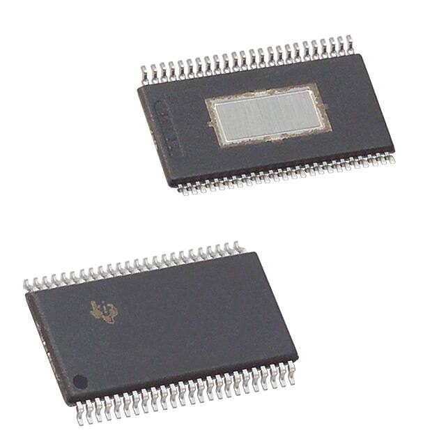


 工商网监
湘ICP备2023018690号
工商网监
湘ICP备2023018690号
