Product
Folder
Order
Now
Support &
Community
Tools &
Software
Technical
Documents
TPL0401A-10-Q1
TPL0401B-10-Q1
SLIS182 – NOVEMBER 2016
TPL0401x-10-Q1 128-TAPS Single-Channel Digital Potentiometer with I2C Interface
1 Features
3 Description
•
•
•
•
•
•
•
•
•
•
•
The TPL0401x-10-Q1 device is a single-channel,
linear-taper digital potentiometer with 128 wiper
positions. The TPL0401x-10-Q1 has the low terminal
internal and connected to GND. The position of the
wiper can be adjusted using an I2C interface. The
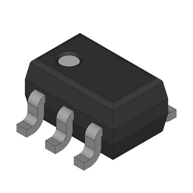
TPL0401x-10-Q1 is available in a 6-pin SC70
package with a specified temperature range of –40°C
to +125°C. The part has a 10-kΩ end-to-end
resistance and can operate with a supply voltage
range of 2.7 V to 5.5 V. This kind of product is widely
used in setting the voltage reference for low power
DDR3 memory.
1
Single-Channel, 128-Position Resolution
10-kΩ End-to-End Resistance Options
Low Temperature Coefficient: 22 ppm/°C
I2C Serial Interface
2.7-V to 5.5-V Single-Supply Operation
±20% Resistance Tolerance
A and B Versions Have Different I2C Addresses
L Terminal is Internal and Connected to GND
Operating Temperature: –40°C to +125°C
Available in Industry Standard SC70 Packages
ESD Performance Tested per JESD 22
– 2000-V Human-Body Model (A114-B, Class II)
The TPL0401x-10-Q1 has the low terminal internal
and connected to GND.
Device Information(1)
2 Applications
•
•
•
•
•
PART NUMBER
TPL0401A-10-Q1
TPL0401B-10-Q1
Mechanical Potentiometer Replacement
Adjustable Power Supplies
Adjustable Gain Amplifiers and Offset Trimming
Precision Calibration of Setpoint Thresholds
Sensor Trimming and Calibration
PACKAGE
SC70 (6)
BODY SIZE (NOM)
2.00 mm × 1.25 mm
(1) For all available packages, see the orderable addendum at
the end of the data sheet.
Simplified Schematic
H
VDD
TPL0401A/B-10-Q1
SCL
SDA
I2C INTERFACE
WIPER
REGISTER
W
GND Copyright © 2016, Texas Instruments Incorporated
1
An IMPORTANT NOTICE at the end of this data sheet addresses availability, warranty, changes, use in safety-critical applications,
intellectual property matters and other important disclaimers. PRODUCTION DATA.
�TPL0401A-10-Q1
TPL0401B-10-Q1
SLIS182 – NOVEMBER 2016
www.ti.com
Table of Contents
1
2
3
4
5
6
7
8
9
Features ..................................................................
Applications ...........................................................
Description .............................................................
Revision History.....................................................
Device Comparison Table.....................................
Pin Configuration and Functions .........................
Specifications.........................................................
1
1
1
2
3
3
4
7.1
7.2
7.3
7.4
7.5
7.6
7.7
4
4
4
4
4
5
7
Absolute Maximum Ratings ......................................
ESD Ratings..............................................................
Recommended Operating Conditions.......................
Thermal Information .................................................
Electrical Characteristics...........................................
Timing Requirements ................................................
Typical Characteristics ..............................................
10 Application and Implementation........................ 21
10.1 Application Information.......................................... 21
10.2 Typical Application ............................................... 21
11 Power Supply Recommendations ..................... 23
11.1
11.2
11.3
11.4
12 Layout................................................................... 25
12.1 Layout Guidelines ................................................. 25
12.2 Layout Example .................................................... 25
13 Device and Documentation Support ................. 26
13.1
13.2
13.3
13.4
13.5
13.6
13.7
Parameter Measurement Information .................. 9
Detailed Description ............................................ 11
9.1
9.2
9.3
9.4
9.5
9.6
Overview .................................................................
Functional Block Diagram .......................................
Feature Description.................................................
Device Functional Modes........................................
Programming...........................................................
Register Maps ........................................................
Power Sequence................................................... 23
Power-On Reset Requirements ........................... 23
I2C Communication After Power Up ..................... 23
Wiper Position While Unpowered and After Power
Up............................................................................. 24
11
11
11
11
15
19
Documentation Support ........................................
Related Links ........................................................
Receiving Notification of Documentation Updates
Community Resources..........................................
Trademarks ...........................................................
Electrostatic Discharge Caution ............................
Glossary ................................................................
26
26
26
26
26
26
26
14 Mechanical, Packaging, and Orderable
Information ........................................................... 27
4 Revision History
2
DATE
REVISION
NOTES
November 2016
*
Initial release.
Submit Documentation Feedback
Copyright © 2016, Texas Instruments Incorporated
Product Folder Links: TPL0401A-10-Q1 TPL0401B-10-Q1
�TPL0401A-10-Q1
TPL0401B-10-Q1
www.ti.com
SLIS182 – NOVEMBER 2016
5 Device Comparison Table
PART NUMBER
END-TO-END RESISTANCE
I2C ADDRESS
TPL0401A-10-Q1
10 kΩ
010 1110 (0×2E)
TPL0401B-10-Q1
10 kΩ
011 1110 (0×3E)
6 Pin Configuration and Functions
DCK Package
6-Pin SC70
Top View
VDD
1
6
H
GND
2
5
W
SCL
3
4
SDA
L
Pin Functions
PIN
NO.
NAME
TYPE
DESCRIPTION
1
VDD
Power
2
GND
—
Positive supply voltage
3
SCL
I
I2C Clock
4
SDA
I/O
I2C Data
5
W
I/O
Wiper terminal
6
H
I/O
High terminal
—
L
I/O
Low terminal (Internally connected to GND)
Ground
Copyright © 2016, Texas Instruments Incorporated
Product Folder Links: TPL0401A-10-Q1 TPL0401B-10-Q1
Submit Documentation Feedback
3
�TPL0401A-10-Q1
TPL0401B-10-Q1
SLIS182 – NOVEMBER 2016
www.ti.com
7 Specifications
7.1 Absolute Maximum Ratings
over operating free-air temperature range (unless otherwise noted)
MIN
MAX
UNIT
–0.3
7
V
±5
mA
Digital input pins (SDA, SCL)
–0.3
VDD + 0.3
Potentiometer pins (H, W)
–0.3
VDD + 0.3
VDD
Supply voltage
IH, IL, IW
Continuous current
VI
VDD to GND
TJ(MAX)
Maximum junction temperature
Tstg
Storage temperature
(1)
(1)
–65
V
130
°C
150
°C
Stresses beyond those listed under Absolute Maximum Ratings may cause permanent damage to the device. These are stress ratings
only, which do not imply functional operation of the device at these or any other conditions beyond those indicated under Recommended
Operating Conditions. Exposure to absolute-maximum-rated conditions for extended periods may affect device reliability.
7.2 ESD Ratings
VALUE
V(ESD)
(1)
Electrostatic discharge
Human-body model (HBM), per AEC Q100-002 (1)
±2500
Charged-device model (CDM), per AEC Q100-011
±1000
UNIT
V
AEC Q100-002 indicates that HBM stressing shall be in accordance with the ANSI/ESDA/JEDEC JS-001 specification.
7.3 Recommended Operating Conditions
over operating free-air temperature range (unless otherwise noted)
VDD
Supply voltage
VW,VH, SDA, SCL
Terminal voltage
VIH
Voltage input high ( SCL, SDA )
VIL
Voltage input low ( SCL, SDA )
IW
Wiper current
TA
Ambient operating temperature
MIN
MAX
2.7
5.5
UNIT
V
0
VDD
V
0.7 × VDD
VDD
V
0
0.3 × VDD
V
–2
2
mA
–40
125
°C
7.4 Thermal Information
TPL0401x-10-Q1
THERMAL METRIC (1)
DCK (SC70)
UNIT
6 PINS
RθJA
Junction-to-ambient thermal resistance
RθJC(top)
Junction-to-case (top) thermal resistance
234
°C/W
110.5
RθJB
°C/W
Junction-to-board thermal resistance
79
°C/W
ψJT
Junction-to-top characterization parameter
7.2
°C/W
ψJB
Junction-to-board characterization parameter
77
°C/W
RθJC(bot)
Junction-to-case (bottom) thermal resistance
N/A
°C/W
(1)
For more information about traditional and new thermal metrics, see the Semiconductor and IC Package Thermal Metrics application
report.
7.5 Electrical Characteristics
Typical values are specified at 25°C and VDD = 3.3 V (unless otherwise noted)
PARAMETER
RTOTAL
End-to-end resistance
RH
Terminal resistance
RW
Wiper resistance
4
Submit Documentation Feedback
TEST CONDITIONS
MIN
8
TYP
MAX
UNIT
10
12
kΩ
100
200
Ω
35
100
Ω
Copyright © 2016, Texas Instruments Incorporated
Product Folder Links: TPL0401A-10-Q1 TPL0401B-10-Q1
�TPL0401A-10-Q1
TPL0401B-10-Q1
www.ti.com
SLIS182 – NOVEMBER 2016
Electrical Characteristics (continued)
Typical values are specified at 25°C and VDD = 3.3 V (unless otherwise noted)
PARAMETER
TEST CONDITIONS
MIN
TYP
MAX
UNIT
CH
Terminal capacitance
10
CW
Wiper capacitance
11
pF
pF
TCR
Resistance temperature coefficient
22
ppm/°C
IDD(STBY)
VDD standby current
IIN-DIG
Digital pins leakage current (SCL,
SDA Inputs)
–40°C to +105°C
0.5
–40°C to +125°C
1.5
µA
–2.5
2.5
µA
0.7 ×
VDD
VDD
V
0
0.3 ×
VDD
V
SERIAL INTERFACE SPECS (SDA, SCL)
VIH
Input high voltage
VIL
Input low voltage
VOL
Output low voltage
SDA Pin, IOL = 4 mA
CIN
Pin capacitance
SCL, SDA Inputs
0.4
V
7
pF
VOLTAGE DIVIDER MODE (VH = VDD, VW = Not Loaded)
INL (1) (2)
Integral non-linearity
DNL (3) (2)
Differential non-linearity
ZSERROR
(4) (5)
–0.5
0.5
LSB
–0.25
0.25
LSB
LSB
Zero-scale error
FSERROR (6) (5) Full-scale error
0
0.75
1.5
–1.5
–0.75
0
LSB
TCV
Ratiometric temperature coefficient Wiper set at mid-scale
4
ppm/°C
BW
Bandwidth
Wiper set at mid-scale,
CLOAD = 10 pF
2862
kHz
TSW
Wiper settling time
See Figure 10
0.152
µs
THD+N
Total harmonic distortion
VH = 1 VRMS at 1 kHz,
measurement at W
0.03
%
RHEOSTAT MODE (VH = VDD, VW = Not Loaded)
RINL (7) (8)
Rheostat mode integral nonlinearity
–1
1
LSB
RDNL (9) (8)
Rheostat mode differential nonlinearity
0.5
0.5
LSB
Rheostat-mode zero-scale error
0
2
LSB
ROFFSET (10) (1
1)
(1)
(2)
(3)
(4)
(5)
(6)
(7)
(8)
(9)
(10)
(11)
0.75
INL = ((VMEAS[code x] – VMEAS[code 0]) / LSB) – [code x]
LSB = (VMEAS[code 127] – VMEAS[code 0]) / 127
DNL = ((VMEAS[code x] – VMEAS[code x-1]) / LSB) – 1
ZSERROR = VMEAS[code 0] / IDEAL_LSB
IDEAL_LSB = VH/ 128
FSERROR = [(VMEAS[code 127] – VH) / IDEAL_LSB] + 1
RINL = ( (RMEAS[code x] – RMEAS[code 0]) / RLSB) – [code x]
RLSB = (RMEAS[code 127] – RMEAS[code 0]) / 127
RDNL = ( (RMEAS[code x] – RMEAS[code x–1]) / RLSB ) – 1
ROFFSET = RMEAS[code 0] / IDEAL_RLSB
IDEAL_RLSB = RTOT / 128
7.6 Timing Requirements
MIN
MAX
UNIT
100
kHz
STANDARD MODE
fSCL
I2C Clock frequency
0
tSCH
I2C Clock high time
4
µs
tSCL
I2C Clock low time
4.7
µs
2
tsp
I C Spike time
tSDS
I2C Serial data setup time
0
250
Copyright © 2016, Texas Instruments Incorporated
Product Folder Links: TPL0401A-10-Q1 TPL0401B-10-Q1
50
ns
ns
Submit Documentation Feedback
5
�TPL0401A-10-Q1
TPL0401B-10-Q1
SLIS182 – NOVEMBER 2016
www.ti.com
Timing Requirements (continued)
MIN
2
MAX
0
UNIT
tSDH
I C Serial data hold time
tICR
I2C Input rise time
1000
ns
tICF
I2C Input fall time
300
ns
300
ns
2
tOCF
I C Output fall time, 10 pF to 400 pF bus
2
ns
tBUF
I C Bus free time between stop and start
4.7
µs
tSTS
I2C Start or repeater start condition setup time
4.7
µs
2
4
µs
2
4
tSTH
I C Start or repeater start condition hold time
tSPS
I C Stop condition setup time
tVD(DATA)
Valid data time, SCL low to SDA output valid
1
µs
µs
tVD(ACK)
Valid data time of ACK condition, ACK signal from SCL low to SDA (out) low
1
µs
FAST MODE
fSCL
tSCH
I2C Clock frequency
0
2
0.6
2
1.3
I C Clock high time
tSCL
I C Clock low time
tsp
I2C Spike time
tSDS
I2C Serial data setup time
0
I C Serial data hold time
tICR
I2C Input rise time
tICF
I2C Input fall time
µs
50
ns
ns
0
2
kHz
µs
100
2
tSDH
400
ns
20
300
ns
20 × (VDD / 5.5)
300
ns
300
tOCF
I C Output fall time, 10 pF to 400 pF bus
(VDD / 5.5) × 20
tBUF
I2C Bus free time between stop and start
1.3
µs
tSTS
I2C Start or repeater start condition setup time
tSTH
ns
1.3
µs
2
0.6
µs
2
0.6
I C Start or repeater start condition hold time
tSPS
I C Stop condition setup time
tVD(DATA)
Valid data time, SCL low to SDA output valid
1
µs
tVD(ACK)
Valid data time of ACK condition, ACK signal from SCL low to SDA (out) low
1
µs
6
Submit Documentation Feedback
µs
Copyright © 2016, Texas Instruments Incorporated
Product Folder Links: TPL0401A-10-Q1 TPL0401B-10-Q1
�TPL0401A-10-Q1
TPL0401B-10-Q1
www.ti.com
SLIS182 – NOVEMBER 2016
7.7 Typical Characteristics
0.15
0.15
2.7 V
3.3 V
5.5 V
0.1
DNL Error (LSB)
INL Error (LSB)
0.1
0.05
0
-0.05
-0.1
0.05
0
-0.05
-0.1
-0.15
-0.15
0
18
36
54
72
Digital Code
90
108
126
0
18
36
54
72
Digital Code
D001
Figure 1. INL vs Tap Position (Potentiometer Mode)
90
108
126
D002
Figure 2. DNL vs Tap Position (Potentiometer Mode)
1
0
2.7 V
3.3 V
5.5 V
2.7 V
3.3 V
5.5 V
-0.1
-0.2
FS Error (LSB)
0.5
RNL Error (LSB)
2.7 V
3.3 V
5.5 V
0
-0.3
-0.4
-0.5
-0.6
-0.7
-0.5
-0.8
-0.9
-1
0
16
32
48
64
80
Digital Code
96
112
-1
-40
128
Figure 3. INL vs Tap Position (Rheostat Mode)
0
20
40
60
Temperature (qC)
80
100
120
D004
Figure 4. Full Scale Error vs Temperature
300
1
2.7 V
3.3 V
5.5 V
2.7 V
3.3 V
5.5 V
270
240
0.5
210
TC (ppm/qC)
Resistance Change ( )
-20
D003
0
180
150
120
90
-0.5
60
30
-1
-40
0
-10
20
50
Temperature (qC)
80
110
130
0
16
32
D005
Figure 5. End-to-End RTOTAL Change vs Temperature
48
64
80
Digital Code
96
112
128
D006
Figure 6. Temperature Coefficient vs TAP Position
(Potentiometer Mode)
Copyright © 2016, Texas Instruments Incorporated
Product Folder Links: TPL0401A-10-Q1 TPL0401B-10-Q1
Submit Documentation Feedback
7
�TPL0401A-10-Q1
TPL0401B-10-Q1
SLIS182 – NOVEMBER 2016
www.ti.com
Typical Characteristics (continued)
300
0
2.7 V
3.3 V
5.5 V
270
240
-6
-12
Magnitude (dB)
TC (ppm/qC)
210
180
150
120
-24
-30
-36
90
-42
60
-48
30
-54
0
0
16
32
48
64
80
Digital Code
96
112
128
Submit Documentation Feedback
-60
103
Code 08
Code 10
Code 20
Code 40
104
105
Frequency (Hz)
D007
Figure 7. Temperature Coefficient vs TAP Position
(Rheostat Mode)
8
-18
106
107
D008
Figure 8. Frequency Response
Copyright © 2016, Texas Instruments Incorporated
Product Folder Links: TPL0401A-10-Q1 TPL0401B-10-Q1
�TPL0401A-10-Q1
TPL0401B-10-Q1
www.ti.com
SLIS182 – NOVEMBER 2016
8 Parameter Measurement Information
VDD
R L = 1 kΏ
SDA
DUT
CL = 50 pF
(see Note A)
SDA LOAD CONFIGURATION
Two Bytes for READ Wiper Position Register
Address
Bit 7
(MSB)
Stop
Start
Condition Condition
(P)
(S)
Address
Bit 1
tscl
R/W
Bit 0
(LSB)
Data
Bit 7
(MSB)
ACK
(A)
Data
Bit 0
(LSB)
Stop
Condition
(P)
tsch
0.7 x VCCI
SCL
0.3 x VCCI
ticr
ticf
tbuf
tvd
tsp
tocf
tvd
tsts
tsps
SDA
0.7 x VCCI
0.3 x VCCI
ticr
ticf
tsdh
tsds
tsth
tvd(ack)
Repeat Start
Condition
Stop
Condition
VOLTAGE WAVEFORMS
BYTE
DESCRIPTION
2
1
I C address
2
Wiper Position Data
A.
CL includes probe and jig capacitance. tocf is measured with CL of 10 pF or 400 pF.
B.
All inputs are supplied by generators having the following characteristics: PRR ≤ 10 MHz, ZO = 50 Ω, tr/tf ≤ 30 ns.
C.
All parameters and waveforms are not applicable to all devices.
Figure 9. I2C Interface Load Circuit and Voltage Waveforms
Copyright © 2016, Texas Instruments Incorporated
Product Folder Links: TPL0401A-10-Q1 TPL0401B-10-Q1
Submit Documentation Feedback
9
�TPL0401A-10-Q1
TPL0401B-10-Q1
SLIS182 – NOVEMBER 2016
www.ti.com
Parameter Measurement Information (continued)
SCL
DATA
ACK
50% VDD
tswx
VW
5% VH
A.
Code change is from 0×40 to 0×00
B.
All inputs are supplied by generators having the following characteristics: PRR ≤ 10 MHz, ZO = 50 Ω, tr/tf ≤ 30 ns.
Figure 10. Switch Time Waveform (tSW)
10
Submit Documentation Feedback
Copyright © 2016, Texas Instruments Incorporated
Product Folder Links: TPL0401A-10-Q1 TPL0401B-10-Q1
�TPL0401A-10-Q1
TPL0401B-10-Q1
www.ti.com
SLIS182 – NOVEMBER 2016
9 Detailed Description
9.1 Overview
The TPL0401x-10-Q1 has a single linear-taper digital potentiometer with 128 wiper positions and an end-to-end
resistance of 10 kΩ. The potentiometer can be used as a three-terminal potentiometer. The main operation of
TPL0401x-10-Q1 is in voltage divider mode.
The low (L) terminal of the TPL0401x-10-Q1 is tied directly to GND. The high (H) and low (GND) terminals of
TPL0401-10-Q1 are equivalent to the fixed terminals of a mechanical potentiometer. The H terminal must have a
higher voltage than the low terminal (GND). The position of the wiper (W) terminal is controlled by the value in
the Wiper Resistance (WR) 8-bit register. When the WR register contains all zeroes (zero-scale), the wiper
terminal is closest to its L terminal. As the value of the WR register increases from all zeroes to all ones (fullscale), the wiper moves from the position closest to the GND terminal to the position closest to the H terminal. At
the same time, the resistance between W and GND increases, whereas the resistance between W and H
decreases.
9.2 Functional Block Diagram
H
VDD
TPL0401A/B-10-Q1
SCL
I2C INTERFACE
SDA
WIPER
REGISTER
W
GND Copyright © 2016, Texas Instruments Incorporated
9.3 Feature Description
The TPL0401x-10-Q1 device is a single-channel, linear taper digital potentiometer with 128 wiper positions.
Default power up state for the TPL0401x-10-Q1 is mid code (0×40). The TPL0401x-10-Q1 has the low terminal
connected to GND internally. The position of the wiper can be adjusted using an I2C interface. The TPL0401x-10Q1 is available in a 6-pin SOT package with a specified temperature range of –40°C to +125°C. The part has a
10-kΩ end-to-end resistance and can operate with a supply voltage range of 2.7 V to 5.5 V. This kind of product
is widely used in setting the voltage reference for low power DDR3 memory. The TPL0401x-10-Q1 has the low
terminal internal and connected to GND.
9.4 Device Functional Modes
9.4.1 Voltage Divider Mode
The digital potentiometer generates a voltage divider when all three terminals are used. The voltage divider at
wiper-to-H and wiper-to-GND is proportional to the input voltage at H to L (see Figure 11).
Copyright © 2016, Texas Instruments Incorporated
Product Folder Links: TPL0401A-10-Q1 TPL0401B-10-Q1
Submit Documentation Feedback
11
�TPL0401A-10-Q1
TPL0401B-10-Q1
SLIS182 – NOVEMBER 2016
www.ti.com
Device Functional Modes (continued)
H
VHW
VH - VL
W
VWL
L
Figure 11. Equivalent Circuit for Voltage Divider Mode
For example, connecting terminal H to 5 V, the output voltage at terminal W can range from 0 V to 5 V.
Equation 1 is the general equation defining the output voltage at terminal W for any valid input voltage applied to
terminal H and terminal L (GND).
VW
VWL
(VH
VL ) u
D
128
(1)
The voltage difference between terminal H and terminal W can also be calculated in Equation 2.
VHW
(VH
§ § D ··
VL ) u ¨ 1 ¨
¸¸
© © 128 ¹ ¹
where
•
D is the decimal value of the wiper code
(2)
Table 1 shows the ideal values for DPOT with end-to end resistance of 10 kΩ. The absolute values of resistance
can vary significantly but the Ratio (RWL/RTOT) is extremely accurate.
The linearity values are relative linearity values (that is, linearity after zero-scale and full-scale offset errors are
removed). Consider this when expecting a certain absolute accuracy because some error is introduced when the
device gets close in magnitude to the offset errors.
Note that the MSB is always discarded during a write to the wiper position register. For example, if 0×80 is
written to the wiper position register, a read returns 0×00. Another similar example is if 0×FF is written, then
0×7F is read.
Table 1. Resistance Values Table
12
STEP
HEX
RWL (KΩ)
RHW (KΩ)
RWL/RTOT
0
0×00
0.00
10.00
0.0%
1
0×01
0.08
9.92
0.8%
2
0×02
0.16
9.84
1.6%
3
0×03
0.23
9.77
2.3%
4
0×04
0.31
9.69
3.1%
5
0×05
0.39
9.61
3.9%
6
0×06
0.47
9.53
4.7%
7
0×07
0.55
9.45
5.5%
8
0×08
0.63
9.38
6.3%
9
0×09
0.70
9.30
7.0%
10
0×0A
0.78
9.22
7.8%
Submit Documentation Feedback
Copyright © 2016, Texas Instruments Incorporated
Product Folder Links: TPL0401A-10-Q1 TPL0401B-10-Q1
�TPL0401A-10-Q1
TPL0401B-10-Q1
www.ti.com
SLIS182 – NOVEMBER 2016
Table 1. Resistance Values Table (continued)
STEP
HEX
RWL (KΩ)
RHW (KΩ)
RWL/RTOT
11
0×0B
0.86
9.14
8.6%
12
0×0C
0.94
9.06
9.4%
13
0×0D
1.02
8.98
10.2%
14
0×0E
1.09
8.91
10.9%
15
0×0F
1.17
8.83
11.7%
16
0×10
1.25
8.75
12.5%
17
0×11
1.33
8.67
13.3%
18
0×12
1.41
8.59
14.1%
19
0×13
1.48
8.52
14.8%
20
0×14
1.56
8.44
15.6%
21
0×15
1.64
8.36
16.4%
22
0×16
1.72
8.28
17.2%
23
0×17
1.80
8.20
18.0%
24
0×18
1.88
8.13
18.8%
25
0×19
1.95
8.05
19.5%
26
0×1A
2.03
7.97
20.3%
27
0×1B
2.11
7.89
21.1%
28
0×1C
2.19
7.81
21.9%
29
0×1D
2.27
7.73
22.7%
30
0×1E
2.34
7.66
23.4%
31
0×1F
2.42
7.58
24.2%
32
0×20
2.50
7.50
25.0%
33
0×21
2.58
7.42
25.8%
34
0×22
2.66
7.34
26.6%
35
0×23
2.73
7.27
27.3%
36
0×24
2.81
7.19
28.1%
37
0×25
2.89
7.11
28.9%
38
0×26
2.97
7.03
29.7%
39
0×27
3.05
6.95
30.5%
40
0×28
3.13
6.88
31.3%
41
0×29
3.20
6.80
32.0%
42
0×2A
3.28
6.72
32.8%
43
0×2B
3.36
6.64
33.6%
44
0×2C
3.44
6.56
34.4%
45
0×2D
3.52
6.48
35.2%
46
0×2E
3.59
6.41
35.9%
47
0×2F
3.67
6.33
36.7%
48
0×30
3.75
6.25
37.5%
49
0×31
3.83
6.17
38.3%
50
0×32
3.91
6.09
39.1%
51
0×33
3.98
6.02
39.8%
52
0×34
4.06
5.94
40.6%
53
0×35
4.14
5.86
41.4%
54
0×36
4.22
5.78
42.2%
55
0×37
4.30
5.70
43.0%
56
0×38
4.38
5.63
43.8%
57
0×39
4.45
5.55
44.5%
Copyright © 2016, Texas Instruments Incorporated
Product Folder Links: TPL0401A-10-Q1 TPL0401B-10-Q1
Submit Documentation Feedback
13
�TPL0401A-10-Q1
TPL0401B-10-Q1
SLIS182 – NOVEMBER 2016
www.ti.com
Table 1. Resistance Values Table (continued)
14
STEP
HEX
RWL (KΩ)
RHW (KΩ)
RWL/RTOT
58
0×3A
4.53
5.47
45.3%
59
0×3B
4.61
5.39
46.1%
60
0×3C
4.69
5.31
46.9%
61
0×3D
4.77
5.23
47.7%
62
0×3E
4.84
5.16
48.4%
63
0×3F
4.92
5.08
49.2%
64 (POR Default)
0×40
5.00
5.00
50.0%
65
0×41
5.08
4.92
50.8%
66
0×42
5.16
4.84
51.6%
67
0×43
5.23
4.77
52.3%
68
0×44
5.31
4.69
53.1%
69
0×45
5.39
4.61
53.9%
70
0×46
5.47
4.53
54.7%
71
0×47
5.55
4.45
55.5%
72
0×48
5.63
4.38
56.3%
73
0×49
5.70
4.30
57.0%
74
0×4A
5.78
4.22
57.8%
75
0×4B
5.86
4.14
58.6%
76
0×4C
5.94
4.06
59.4%
77
0×4D
6.02
3.98
60.2%
78
0×4E
6.09
3.91
60.9%
79
0×4F
6.17
3.83
61.7%
80
0×50
6.25
3.75
62.5%
81
0×51
6.33
3.67
63.3%
82
0×52
6.41
3.59
64.1%
83
0×53
6.48
3.52
64.8%
84
0×54
6.56
3.44
65.6%
85
0×55
6.64
3.36
66.4%
86
0×56
6.72
3.28
67.2%
87
0×57
6.80
3.20
68.0%
88
0×58
6.88
3.13
68.8%
89
0×59
6.95
3.05
69.5%
90
0×5A
7.03
2.97
70.3%
91
0×5B
7.11
2.89
71.1%
92
0×5C
7.19
2.81
71.9%
93
0×5D
7.27
2.73
72.7%
94
0×5E
7.34
2.66
73.4%
95
0×5F
7.42
2.58
74.2%
96
0×60
7.50
2.50
75.0%
97
0×61
7.58
2.42
75.8%
98
0×62
7.66
2.34
76.6%
99
0×63
7.73
2.27
77.3%
100
0×64
7.81
2.19
78.1%
101
0×65
7.89
2.11
78.9%
102
0×66
7.97
2.03
79.7%
103
0×67
8.05
1.95
80.5%
104
0×68
8.13
1.88
81.3%
Submit Documentation Feedback
Copyright © 2016, Texas Instruments Incorporated
Product Folder Links: TPL0401A-10-Q1 TPL0401B-10-Q1
�TPL0401A-10-Q1
TPL0401B-10-Q1
www.ti.com
SLIS182 – NOVEMBER 2016
Table 1. Resistance Values Table (continued)
STEP
HEX
RWL (KΩ)
RHW (KΩ)
RWL/RTOT
105
0×69
8.20
1.80
82.0%
106
0×6A
8.28
1.72
82.8%
107
0×6B
8.36
1.64
83.6%
108
0×6C
8.44
1.56
84.4%
109
0×6D
8.52
1.48
85.2%
110
0×6E
8.59
1.41
85.9%
111
0×6F
8.67
1.33
86.7%
112
0×70
8.75
1.25
87.5%
113
0×71
8.83
1.17
88.3%
114
0×72
8.91
1.09
89.1%
115
0×73
8.98
1.02
89.8%
116
0×74
9.06
0.94
90.6%
117
0×75
9.14
0.86
91.4%
118
0×76
9.22
0.78
92.2%
119
0×77
9.30
0.70
93.0%
120
0×78
9.38
0.63
93.8%
121
0×79
9.45
0.55
94.5%
122
0×7A
9.53
0.47
95.3%
123
0×7B
9.61
0.39
96.1%
124
0×7C
9.69
0.31
96.9%
125
0×7D
9.77
0.23
97.7%
126
0×7E
9.84
0.16
98.4%
127
0×7F
9.92
0.08
99.2%
9.5 Programming
9.5.1 I2C General Operation and Overview
9.5.1.1 START and STOP Conditions
I2C communication with this device is initiated by the master sending a START condition and terminated by the
master sending a STOP condition. A high-to-low transition on the SDA line while the SCL is high defines a
START condition. A low-to-high transition on the SDA line while the SCL is high defines a STOP condition. See
Figure 12.
SCL
SDA
START
Condition
Data Transfer
STOP
Condition
Figure 12. Definition of START and STOP Conditions
Copyright © 2016, Texas Instruments Incorporated
Product Folder Links: TPL0401A-10-Q1 TPL0401B-10-Q1
Submit Documentation Feedback
15
�TPL0401A-10-Q1
TPL0401B-10-Q1
SLIS182 – NOVEMBER 2016
www.ti.com
Programming (continued)
9.5.1.2 Data Validity and Byte Formation
One data bit is transferred during each clock pulse of the SCL. One byte is comprised of eight bits on the SDA
line. See Figure 13. A byte may either be a device address, register address, or data written to or read from a
slave.
Data is transferred Most Significant Bit (MSB) first. Any number of data bytes can be transferred from the master
to slave between the START and STOP conditions. Data on the SDA line must remain stable during the high
phase of the clock period, as changes in the data line when the SCL is high are interpreted as control commands
(START or STOP).
SDA line stable while SCL line is high
SCL
1
0
1
0
1
0
1
0
ACK
MSB
Bit
Bit
Bit
Bit
Bit
Bit
LSB
ACK
SDA
Byte: 1010 1010 ( 0xAAh )
Figure 13. Definition of Byte Formation
9.5.1.3 Acknowledge (ACK) and Not Acknowledge (NACK)
Each byte is followed by one ACK bit from the receiver. The ACK bit allows the receiver to communicate to the
transmitter that the byte was successfully received and another byte may be sent.
The transmitter must release the SDA line before the receiver can send the ACK bit. To send an ACK bit, the
receiver shall pull down the SDA line during the low phase of the ACK/NACK-related clock period (period 9), so
that the SDA line is stable low during the high phase of the ACK/NACK-related clock period. Consider setup and
hold times. Figure 14 shows an example use of ACK.
16
Submit Documentation Feedback
Copyright © 2016, Texas Instruments Incorporated
Product Folder Links: TPL0401A-10-Q1 TPL0401B-10-Q1
�TPL0401A-10-Q1
TPL0401B-10-Q1
www.ti.com
SLIS182 – NOVEMBER 2016
Programming (continued)
1
2
3
4
5
6
7
MSB
A6
A5
A4
A3
A2
A1
A0
SCL
8
9
SDA
START
Condition
LSB
ACK
R/W
Device Address
Figure 14. Example Use of ACK
When the SDA line remains high during the ACK/NACK-related clock period, this is a NACK signal. There are
several conditions that lead to the generation of a NACK:
• The receiver is unable to receive or transmit because it is performing some real-time function and is not ready
to start communication with the master.
• During the transfer, the receiver gets data or commands that it does not understand.
• During the transfer, the receiver cannot receive any more data bytes.
• A master-receiver is done reading data and indicates this to the slave through a NACK.
Figure 15 shows an example use of NACK.
SCL
1
2
3
4
5
6
7
8
9
D6
D5
D4
D3
D2
D1
LSB
D0
NACK
SDA
MSB
D7
STOP
Condition
Data Byte N
Figure 15. Example Use of NACK
9.5.1.4 Repeated Start
A repeated START condition may be used in place of a complete STOP condition follow by another START
condition when performing a read function. The advantage of this is that the I2C bus does not become available
after the stop and therefore prevents other devices from grabbing the bus between transfers.
Copyright © 2016, Texas Instruments Incorporated
Product Folder Links: TPL0401A-10-Q1 TPL0401B-10-Q1
Submit Documentation Feedback
17
�TPL0401A-10-Q1
TPL0401B-10-Q1
SLIS182 – NOVEMBER 2016
www.ti.com
Programming (continued)
9.5.2 Programing With I2C
9.5.2.1 Write Operation
To write on the I2C bus, the master sends a START condition on the bus with the address of the slave, as well
as the last bit (the R/W bit) set to 0, which signifies a write. After the slave responds with an acknowledge, the
master then sends the register address of the register to which it wishes to write. The slave acknowledges again,
letting the master know that it is ready. After this, the master starts sending the register data to the slave until the
master has sent all the data necessary (which is sometimes only a single byte), and the master terminates the
transmission with a STOP condition. See Figure 16.
Master controls SDA line
Slave controls SDA line
Write to one register in a device
Register Address N (8 bits)
Device (Slave) Address (7 bits)
S
A6 A5 A4 A3 A2 A1 A0
START
0
R/W=0
A
B7 B6 B5 B4 B3 B2 B1 B0
ACK
Data Byte to Register N (8 bits)
A
D7 D6 D5 D4 D3 D2 D1 D0
ACK
A
ACK
P
STOP
Figure 16. Write Operation
9.5.2.2 Read Operation
Reading from a slave is very similar to writing, but requires some additional steps. in order to read from a slave,
the master must first instruct the slave which register it wishes to read from. This is done by the master starting
off the transmission in a similar fashion as the write, by sending the address with the R/W bit equal to 0
(signifying a write), followed by the register address it wishes to read from. When the slave acknowledges this
register address, the master sends a START condition again, followed by the slave address with the R/W bit set
to 1 (Signifying a read). This time, the slave acknowledges the read request, and the master releases the SDA
bus but continues supplying the clock to the slave. During this part of the transaction, the master becomes the
master-receiver, and the slave becomes the slave-transmission.
The master continues to send out the clock pulses, for each byte of data that it wishes to receive. At the end of
every byte of data, the master sends an ACK to the slave, letting the slave know that it is ready for more data.
When the master has received the number of bytes it was expecting (or needs to stop communication), it sends
a NACK, signaling to the slave to halt communications and release the bus. The master follows this up with a
STOP condition. Figure 17 shows the read operation from one register.
18
Submit Documentation Feedback
Copyright © 2016, Texas Instruments Incorporated
Product Folder Links: TPL0401A-10-Q1 TPL0401B-10-Q1
�TPL0401A-10-Q1
TPL0401B-10-Q1
www.ti.com
SLIS182 – NOVEMBER 2016
Programming (continued)
Read from one register in a device
Register Address N (8 bits)
Device (Slave) Address (7 bits)
S
A6 A5 A4 A3 A2 A1 A0
START
0
R/W=0
A
Data Byte from Register N (8 bits)
Device (Slave) Address (7 bits)
B7 B6 B5 B4 B3 B2 B1 B0
A
P
S
ACK STOP START
ACK
1
A6 A5 A4 A3 A2 A1 A0
A
D7 D6 D5 D4 D3 D2 D1 D0 NA
ACK
R/W=1
NACK
P
STOP
Read from one register in a device (Repeated Start)
Device (Slave) Address (7 bits)
S
A6 A5 A4 A3 A2 A1 A0
0
R/W=0
START
A
B7
Data Byte from Register N (8 bits)
Device (Slave) Address (7 bits)
Register Address N (8 bits)
B6 B5 B4 B3 B2 B1 B0
A
ACK
ACK
Sr
A6 A5 A4 A3 A2 A1 A0
Repeated START
1
A
R/W=1
D7 D6 D5 D4 D3 D2 D1 D0 NA
ACK
NACK
P
STOP
Figure 17. Read Operation from One Register
Read from one register in a device with single register
Data Byte from Register (8 bits)
Device (Slave) Address (7 bits)
S
A6 A5 A4 A3 A2 A1 A0
START
1
A
R/W=1
D7 D6 D5 D4 D3 D2 D1 D0 NA
ACK
NACK
P
STOP
Figure 18. Short Read Operation
The TPL0401x-10-Q1 has 1 register, and it is not a requirement that the register address be sent before a read.
A shorter read allows the user to simply send a read request to the device address as shown in Figure 18.
9.6 Register Maps
9.6.1 Slave Address
Table 2 and Table 3 show the TPL0401A-10-Q1 and TPL0401B-10-Q1 bit address repectively.
Table 2. TPL0401A-10-Q1 Bit Address
BIT 7
(MSB)
0
BIT 6
BIT 5
BIT 4
BIT 3
BIT 2
BIT 1
1
0
1
1
1
0
BIT 7
(MSB)
0
BIT 6
BIT 5
BIT 4
BIT 3
BIT 2
BIT 1
1
1
1
1
1
0
BIT 0
(LSB)
R/W
Table 3. TPL0401B-10-Q1 Bit Address
Copyright © 2016, Texas Instruments Incorporated
Product Folder Links: TPL0401A-10-Q1 TPL0401B-10-Q1
BIT 0
(LSB)
R/W
Submit Documentation Feedback
19
�TPL0401A-10-Q1
TPL0401B-10-Q1
SLIS182 – NOVEMBER 2016
www.ti.com
9.6.2 Register Address
Following the successful acknowledgment of the address byte, the bus master sends a command byte as shown
in Figure 19, which is stored in the Control Register in the TPL0401x-10-Q1. The TPL0401x-10-Q1 has only 1
register, but requires the command byte be sent during communication.
B7
B6
B5
B4
B3
B2
B1
B0
Figure 19. Register Address Byte
Table 4 shows the TPL0401x-10-Q1 register address byte.
Table 4. Register Address Byte
REGISTER ADDRESS BITS
B7
B6
B5
B4
B3
B2
B1
B0
REGISTER
ADDRESS
(HEX)
0
0
0
0
0
0
0
0
0×00
REGISTER
PROTOCOL
POWER-UP
DEFAULT
Wiper Position
Read/Write byte
0100 0000
(0×40)
See Table 1 for more information on the wiper position register values. Note that the MSB is always discarded
during a write to the wiper position register. For example, if 0×80 is written to the wiper position register, a read
returns 0×00. Another similar example is if 0×FF is written, then 0×7F is read.
20
Submit Documentation Feedback
Copyright © 2016, Texas Instruments Incorporated
Product Folder Links: TPL0401A-10-Q1 TPL0401B-10-Q1
�TPL0401A-10-Q1
TPL0401B-10-Q1
www.ti.com
SLIS182 – NOVEMBER 2016
10 Application and Implementation
10.1 Application Information
There are many applications in which voltage division is needed through the use of a digital potentiometer such
as the TPL0401x-10-Q1; this is one example of the many. In conjunction with many amplifiers, the TPL0401x-10Q1 can effectively be used in voltage divider mode to create a buffer to adjust the reference voltage for DDR3
DIMM1 Memory.
10.2 Typical Application
1.5 V
+
1 kŸ
DDR3 DIMM1
VREF
-
DPOT
TPL0401A/B-10-Q1
1 kŸ
OP-AMP
Copyright © 2016, Texas Instruments Incorporated
Figure 20. DDR3 Voltage Reference Adjustment
10.2.1 Design Requirements
Table 5 lists the design parameters for this example.
Table 5. Design Parameters
PARAMETER
EXAMPLE VALUE
Input voltage
1.5 V
VREF
0 V to 0.75 V
10.2.2 Detailed Design Procedure
The TPL0401x-10-Q1 can be used in voltage divider mode with a unity-gain op amp buffer to provide a clean
voltage reference for DDR3 DIMM1 Memory. The analog output voltage, VREF1 is determined by the wiper setting
programmed through the I2C bus.
The op amp is required to buffer the high-impedance output of the TPL0401x-10-Q1 or else loading placed on
the output of the voltage divider affects the output voltage.
Copyright © 2016, Texas Instruments Incorporated
Product Folder Links: TPL0401A-10-Q1 TPL0401B-10-Q1
Submit Documentation Feedback
21
�TPL0401A-10-Q1
TPL0401B-10-Q1
SLIS182 – NOVEMBER 2016
www.ti.com
10.2.3 Application Curve
The voltage, 1.5 V, applied to terminal H of TPL0401x-10-Q1 determines the voltage that is buffered by the unitygain op amp and divided as the DDR3 DIMM1 voltage reference. By using the TPL0401x-10-Q1, and dividing the
1.5 V, a maximum of 0.75 V is applied to the buffer and passed to the voltage divider. The output voltage then
ranges from 0 V to 0.75 V.
0.8
VREF (V)
0.6
0.4
0.2
0
0
8
16
24
32
40
48
56
64
72
80
TPL0401A/B Code (Digital Input)
88
96
104
112
120
128
D001
Figure 21. TPL0401-10-Q1 Digital Input vs Reference Voltage for DDR3 DIMM Memory
22
Submit Documentation Feedback
Copyright © 2016, Texas Instruments Incorporated
Product Folder Links: TPL0401A-10-Q1 TPL0401B-10-Q1
�TPL0401A-10-Q1
TPL0401B-10-Q1
www.ti.com
SLIS182 – NOVEMBER 2016
11 Power Supply Recommendations
11.1 Power Sequence
Protection diodes limit the voltage compliance at SDA, SCL, terminal H, and terminal W, making it important to
power up VDD first before applying any voltage to SDA, SCL, terminal H, and terminal W. The diodes are forwardbiasing, meaning VDD can be powered unintentionally if VDD is not powered first. The ideal power-up sequence is
VDD, digital inputs, and VW and VH. The order of powering digital inputs, VH and VW does not matter as long as
they are powered after VDD.
11.2 Power-On Reset Requirements
In the event of a glitch or data corruption, the TPL0401-10-Q1 can be reset to its default conditions by using the
power-on reset feature. Power-on reset requires that the device go through a power cycle to be completely reset.
This reset also happens when the device is powered on for the first time in an application.
VDD
Ramp-Up
Ramp-Down
Re-Ramp-Up
tTRR_GND
Time
tRT
Time to Re-Ramp
tFT
tRT
Figure 22. VDD is Lowered to 0 V and then Ramped Up to VDD
Table 6 specifies the performance of the power-on reset feature for the TPL0401-10-Q1 for both types of poweron reset.
Table 6. Recommended Supply Sequencing and Ramp Rates at TA = 25°C (1)
PARAMETER
MIN
MAX
UNIT
tFT
Fall rate
See Figure 22
0.0001
1000
ms
tRT
Rise rate
See Figure 22
0.0001
1000
ms
tRR_GND
Time to re-ramp (when VDD drops to GND)
See Figure 22
1
(1)
μs
Not tested. Specified by design.
11.3 I2C Communication After Power Up
In order to ensure a complete device reset after a power up condition, the user must wait 120 µs after power up
before initiating communication with the TPL0401x-10-Q1. See Figure 23 for an example waveform.
VDD
VDD MIN
120 µ sx
SDA
START
ADDR
Figure 23. Recommended Start Up Sequence
Copyright © 2016, Texas Instruments Incorporated
Product Folder Links: TPL0401A-10-Q1 TPL0401B-10-Q1
Submit Documentation Feedback
23
�TPL0401A-10-Q1
TPL0401B-10-Q1
SLIS182 – NOVEMBER 2016
www.ti.com
11.4 Wiper Position While Unpowered and After Power Up
When DPOT is powered off, the impedance of the device is undefined and not known.
Upon power-up, the device returns to 0×40h code because this device does not contain non-volatile memory.
24
Submit Documentation Feedback
Copyright © 2016, Texas Instruments Incorporated
Product Folder Links: TPL0401A-10-Q1 TPL0401B-10-Q1
�TPL0401A-10-Q1
TPL0401B-10-Q1
www.ti.com
SLIS182 – NOVEMBER 2016
12 Layout
12.1 Layout Guidelines
To
•
•
•
•
•
•
•
•
ensure reliability of the device, follow common printed-circuit board (PCB) layout guidelines:
Leads to the input must be as direct as possible with a minimum conductor length.
The ground path must have low resistance and low inductance.
Use short trace-lengths to avoid excessive loading.
It is common to have a dedicated ground plane on an inner layer of the board.
Terminals that are connected to ground must have a low-impedance path to the ground plane in the form of
wide polygon pours and multiple vias.
Use bypass capacitors on power supplies and placed them as close as possible to the VDD pin.
Apply low equivalent series resistance (0.1-μF to 10-μF tantalum or electrolytic capacitors) at the supplies to
minimize transient disturbances and to filter low-frequency ripple.
To reduce the total I2C bus capacitance added by PCB parasitics, data lines (SCL and SDA) must be as short
as possible and the widths of the traces must also be minimized (for example, 5 to 10 mils depending on
copper weight).
12.2 Layout Example
Via to VDD Power Plane
0402 Cap
0603 Cap
Via to GND Plane
H
VDD
GND
SCL
TPL0401A/B-10-Q1
W
SDA
Figure 24. Layout Recommendation
Copyright © 2016, Texas Instruments Incorporated
Product Folder Links: TPL0401A-10-Q1 TPL0401B-10-Q1
Submit Documentation Feedback
25
�TPL0401A-10-Q1
TPL0401B-10-Q1
SLIS182 – NOVEMBER 2016
www.ti.com
13 Device and Documentation Support
13.1 Documentation Support
13.1.1 Related Documentation
For related documentation see the following:
• I2C Bus Pullup Resistor Calculation
• Understanding the I2C Bus
• TPL0401 Evaluation Module User's Guide
13.2 Related Links
The table below lists quick access links. Categories include technical documents, support and community
resources, tools and software, and quick access to sample or buy.
Table 7. Related Links
PARTS
PRODUCT FOLDER
SAMPLE & BUY
TECHNICAL
DOCUMENTS
TOOLS &
SOFTWARE
SUPPORT &
COMMUNITY
TPL0401A-Q1
Click here
Click here
Click here
Click here
Click here
TPL0401B-Q1
Click here
Click here
Click here
Click here
Click here
13.3 Receiving Notification of Documentation Updates
To receive notification of documentation updates, navigate to the device product folder on ti.com. In the upper
right corner, click on Alert me to register and receive a weekly digest of any product information that has
changed. For change details, review the revision history included in any revised document.
13.4 Community Resources
The following links connect to TI community resources. Linked contents are provided "AS IS" by the respective
contributors. They do not constitute TI specifications and do not necessarily reflect TI's views; see TI's Terms of
Use.
TI E2E™ Online Community TI's Engineer-to-Engineer (E2E) Community. Created to foster collaboration
among engineers. At e2e.ti.com, you can ask questions, share knowledge, explore ideas and help
solve problems with fellow engineers.
Design Support TI's Design Support Quickly find helpful E2E forums along with design support tools and
contact information for technical support.
13.5 Trademarks
E2E is a trademark of Texas Instruments.
All other trademarks are the property of their respective owners.
13.6 Electrostatic Discharge Caution
This integrated circuit can be damaged by ESD. Texas Instruments recommends that all integrated circuits be handled with
appropriate precautions. Failure to observe proper handling and installation procedures can cause damage.
ESD damage can range from subtle performance degradation to complete device failure. Precision integrated circuits may be more
susceptible to damage because very small parametric changes could cause the device not to meet its published specifications.
13.7 Glossary
SLYZ022 — TI Glossary.
This glossary lists and explains terms, acronyms, and definitions.
26
Submit Documentation Feedback
Copyright © 2016, Texas Instruments Incorporated
Product Folder Links: TPL0401A-10-Q1 TPL0401B-10-Q1
�TPL0401A-10-Q1
TPL0401B-10-Q1
www.ti.com
SLIS182 – NOVEMBER 2016
14 Mechanical, Packaging, and Orderable Information
The following pages include mechanical, packaging, and orderable information. This information is the most
current data available for the designated devices. This data is subject to change without notice and revision of
this document. For browser-based versions of this data sheet, refer to the left-hand navigation.
Copyright © 2016, Texas Instruments Incorporated
Product Folder Links: TPL0401A-10-Q1 TPL0401B-10-Q1
Submit Documentation Feedback
27
�PACKAGE OPTION ADDENDUM
www.ti.com
10-Dec-2020
PACKAGING INFORMATION
Orderable Device
Status
(1)
Package Type Package Pins Package
Drawing
Qty
Eco Plan
(2)
Lead finish/
Ball material
MSL Peak Temp
Op Temp (°C)
Device Marking
(3)
(4/5)
(6)
TPL0401A-10QDCKRQ1
ACTIVE
SC70
DCK
6
3000
RoHS & Green
NIPDAU
Level-2-260C-1 YEAR
-40 to 125
15N
TPL0401B-10QDCKRQ1
ACTIVE
SC70
DCK
6
3000
RoHS & Green
NIPDAU
Level-2-260C-1 YEAR
-40 to 125
15O
(1)
The marketing status values are defined as follows:
ACTIVE: Product device recommended for new designs.
LIFEBUY: TI has announced that the device will be discontinued, and a lifetime-buy period is in effect.
NRND: Not recommended for new designs. Device is in production to support existing customers, but TI does not recommend using this part in a new design.
PREVIEW: Device has been announced but is not in production. Samples may or may not be available.
OBSOLETE: TI has discontinued the production of the device.
(2)
RoHS: TI defines "RoHS" to mean semiconductor products that are compliant with the current EU RoHS requirements for all 10 RoHS substances, including the requirement that RoHS substance
do not exceed 0.1% by weight in homogeneous materials. Where designed to be soldered at high temperatures, "RoHS" products are suitable for use in specified lead-free processes. TI may
reference these types of products as "Pb-Free".
RoHS Exempt: TI defines "RoHS Exempt" to mean products that contain lead but are compliant with EU RoHS pursuant to a specific EU RoHS exemption.
Green: TI defines "Green" to mean the content of Chlorine (Cl) and Bromine (Br) based flame retardants meet JS709B low halogen requirements of


 工商网监
湘ICP备2023018690号
工商网监
湘ICP备2023018690号