User's Guide
SNAU174 – January 2015
TPL5110 Evaluation Module
This user's guide provides the setup instructions, configuration, and operation of the TPL5110 evaluation
module (EVM). Also included are the printed-circuit board (PCB) layouts, schematic, and the bill of
materials (BOM).
1
2
3
4
5
6
Contents
Introduction ................................................................................................................... 2
Setup .......................................................................................................................... 3
2.1
Jumpers and Connectors .......................................................................................... 3
2.2
Battery Requirements .............................................................................................. 5
2.3
TPL5110EVM Configuration ....................................................................................... 5
Operation .................................................................................................................... 10
3.1
Supply Current Measurement ................................................................................... 11
Board Layout ................................................................................................................ 14
Schematic ................................................................................................................... 16
Bill of Materials ............................................................................................................. 17
List of Figures
................................................................................................................ 2
........................................................................................................... 3
J1 Jumper Setting ........................................................................................................... 3
I_SEL Jumper Setting ....................................................................................................... 4
R_SEL Jumper Setting ...................................................................................................... 4
MODE Jumper Setting ...................................................................................................... 4
Jumpers Configuration – EVM Standalone Without Microcontroller .................................................. 6
Jumpers Configuration – EVM With Microcontroller .................................................................... 7
Jumpers Configuration – EVM With LaunchPad ........................................................................ 8
Current Measurement Setup – TPL5110 only .......................................................................... 11
Current Measurement Setup – TPL5110 During the Reading of the Resistance .................................. 12
Current Measurement Setup – TPL5110 With Microcontroller ....................................................... 13
Top Layer.................................................................................................................... 14
Bottom Layer ................................................................................................................ 15
TPL5110EVM Schematic.................................................................................................. 16
1
TPL5110EVM
2
J1 Jumper Setting
3
4
5
6
7
8
9
10
11
12
13
14
15
List of Tables
1
Device and Package Configurations ...................................................................................... 2
2
Input/Output Connectors Description...................................................................................... 3
3
Jumpers Description ......................................................................................................... 3
4
Switches and Selectors Description ....................................................................................... 4
5
Test Points Description
6
..................................................................................................... 4
TPL5110EVM Bill of Materials ............................................................................................ 17
LaunchPad is a trademark of Texas Instruments.
DURACELL is a registered trademark of The Gillette Company.
SNAU174 – January 2015
Submit Documentation Feedback
TPL5110 Evaluation Module
Copyright © 2015, Texas Instruments Incorporated
1
�Introduction
1
www.ti.com
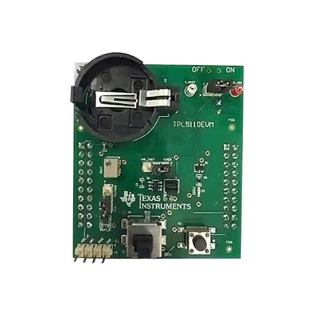
Introduction
I_SEL
J1/J3
J4/J2
MODE
REXT
Q1
J1
R_SEL
U1
REXT1
REXT2
IO
MANUAL_DRV
DONE
Figure 1. TPL5110EVM
TI's TPL5110EVM evaluation module (EVM) allows a designer to configure the timer intervals of the
TPL5110 and measure its very low current consumption. Moreover, the TPL5110EVM is ready to be
connected to the LaunchPad™ of the MSP430F5529 in order to test its power gating and timer features.
The EVM has an onboard battery holder (coin battery) to supply the TPL5110 and the microcontroller, if
connected.
The EVM contains one TPL5110 converter (see Table 1).
Table 1. Device and Package Configurations
2
Device
IC
Package
U1
TPL5110DDC
SOT23-6
TPL5110 Evaluation Module
SNAU174 – January 2015
Submit Documentation Feedback
Copyright © 2015, Texas Instruments Incorporated
�Setup
www.ti.com
2
Setup
Section 2.1 describes the jumpers and connectors on the EVM and Section 2.3 describes how to properly
connect, set up, and use the TPL5110EVM.
See Figure 1 for locations of the top layer jumpers and switches.
2.1
Jumpers and Connectors
Table 2 through Table 5 list the input/output connectors description, jumpers description, switches and
selectors description, and the test points description.
Table 2. Input/Output Connectors Description
Name
Layer
Description
J1/J3
Bottom
2 × 10 pin receptacle to plug the TPL5010EVM into the MSP430F5529 LaunchPad
J4/J2
Bottom
2 × 10 pin receptacle to plug the TPL5010EVM into the MSP430F5529 LaunchPad
RST
Bottom
2-pin receptacle to plug the TPL5010EVM into the MSP430F5529 LaunchPad
VCC
Bottom
2-pin receptacle to plug the TPL5010EVM into the MSP430F5529 LaunchPad
IO
Top
4-pin header connector to bring out RSTn, WAKE, DONE, and GND signals
IO.1
GND
Ground
IO.2
DONE
DONE signal from external microcontroller
IO.3
DRV
DRV signal to control external MOSFET
IO.4
VDD_uC Power gated supply voltage to external microcontroller
Table 3. Jumpers Description
Name
Layer
J1
Top
Description
J1.5–J1.3 shorted, the DRV pin of the TPL5110 is connected to the gate of Q1 MOSFET.
J1.3–J1.1 shorted, the gate of Q1 MOSFET is connected to VDD (MOSFET OFF).
J1
J1
DRV
Connected
to Q1
Q1 OFF
Figure 2. J1 Jumper Setting
J1.6–J1.4 shorted, the DONE pin of the TPL5110 is connected to the S2 switch with pull-down
resistor.
J1.4–J1.2 shorted, the DONE pin of the TPL5110 is connected to GND.
J1
J1
J1
DONE
Connected
to S2
DONE
Connected
to GND
DONE
Connected
to IO
Figure 3. J1 Jumper Setting
SNAU174 – January 2015
Submit Documentation Feedback
TPL5110 Evaluation Module
Copyright © 2015, Texas Instruments Incorporated
3
�Setup
www.ti.com
Table 3. Jumpers Description (continued)
Name
Layer
I_SEL
Top
Description
In open configuration, allows the measurement of the current consumption of the TPL5110.
I_SEL
Normal
Operation
I_SEL
TPL5110 Current
Measurement
Figure 4. I_SEL Jumper Setting
R_SEL
Top
Pin1-2 in short configuration, the variable resistance is used to set the timer interval.
Pin2-3 in short configuration, the fix resistance is used to set the timer interval.
R_SEL
R_SEL
Variable
Resistance
Fix
Resistance
Figure 5. R_SEL Jumper Setting
MODE
Top
Pin1-2 in short configuration, TPL5110 in timer mode.
Pin2-3 in short configuration, TPL5110 in one-shot mode.
MODE
MODE
One-Shot
Mode
Timer
Mode
Figure 6. MODE Jumper Setting
Table 4. Switches and Selectors Description
Name
Layer
Description
S_ON_OFF
Bottom
In ON position turns ON the EVM, in OFF position turns OFF the EVM
S1
Top
When pushed, the SPST switch generates a DONE pulse
S2
Top
When pushed, the SPDT ON/Momentary switch generates a manual
MOSFET drive pulse
Table 5. Test Points Description
4
Name
Layer
Description
GND
Top
Test point of the ground, connect the GND of the power supplies here
V_BATT
Top
Test point to monitor battery voltage
AUX_VDD
Top
Test point to connect external supply voltage in alternative to the coin
cell battery
TPL5110 Evaluation Module
SNAU174 – January 2015
Submit Documentation Feedback
Copyright © 2015, Texas Instruments Incorporated
�Setup
www.ti.com
2.2
Battery Requirements
In
•
•
•
•
case the EVM is battery powered, the battery must meet the following requirements:
Battery type: CR2032 UL-certified battery
Voltage: 3 V
Min capacity: 220 mAh
Min discharge rate: N/A mA
NOTE: Only insert DURACELL® 2032 lithium battery type CR2032, or equivalent.
2.3
TPL5110EVM Configuration
The evaluation board can work standalone or plugged into the MSP430F5529 LaunchPad.
2.3.1
Setting the DRV Pulse Interval
Set the DRV pulse interval by tuning the variable resistance (the trimmer can generate resistances in the
range between 1 kΩ and 200 kΩ).
To
1.
2.
3.
tune the value of the resistance:
Connect a DMM between pin 1 of R_SEL and GND.
Turn the screw on the top of the trimmer until you reach the desired value.
Disconnect the DMM at the end of the operation.
Alternatively, set the DRV pulse interval with the fix resistances (R_EXT1 = 500 Ω, R_EXT2 = 0 Ω). If
required, replace the resistances with customized ones.
See Figure 1 for locations of the resistances REXT1 and REXT2
SNAU174 – January 2015
Submit Documentation Feedback
TPL5110 Evaluation Module
Copyright © 2015, Texas Instruments Incorporated
5
�Setup
www.ti.com
2.3.2
EVM Standalone Without Microcontroller
The following settings are provided to use the EVM standalone, without a microcontroller:
• Put the S_ON_OFF selector in the OFF position.
• Set the mode of operation through the MODE header (see Table 3).
• Insert a CR2032 coin cell battery in the battery holder (BT), alternatively, connect a voltage source
between the AUX_VDD and GND test points.
• Configure jumper J1 (DRV connected to Q1, DONE connected to S2), as explained in Table 3.
NOTE: Do not connect the coin cell battery and the voltage source to supply the evaluation board at
same time.
•
Put the S_ON_OFF selector in the ON position, or turn on the external voltage source if it is used
instead of the coin cell battery.
The DONE and DRV signals can be monitored at the IO connector (pin 2 and 3, respectively).
S_ON_OFF
CR2032
I_SEL
MODE
J1
R_SEL
xx
xx
xx
x
IO
x
x
x
x
x
x
DRV DONE
Figure 7. Jumpers Configuration – EVM Standalone Without Microcontroller
6
TPL5110 Evaluation Module
SNAU174 – January 2015
Submit Documentation Feedback
Copyright © 2015, Texas Instruments Incorporated
�Setup
www.ti.com
2.3.3
EVM With Microcontroller
The following settings are provided to use the EVM with a microcontroller:
• Put the S_ON_OFF selector in the OFF position.
• Set the mode of operation through the MODE header (see Table 3).
• Connect the microcontroller to the IO header, in order to manage the I/O signal of the design under
test (DUT).
• Insert a CR2032 coin cell battery in the battery holder (BT), alternatively, connect a voltage source
between the V_BATT and GND test points.
• Configure jumper J1 (DRV connected to Q1, DONE connected to IO), as explained in Table 3.
NOTE: Do not connect the coin cell battery and the voltage source to supply the evaluation board at
the same time.
Do not use the switch S2 (DONE), in this configuration the DONE switch is connected to a
digital output pin of the microcontroller.
•
Put the S_ON_OFF selector in the ON position, or turn on the external voltage source if it is used
instead of the coin cell battery.
S_ON_OFF
CR2032
I_SEL
MODE
J1
R_SEL
µC
GND GPIO
VDD
VDD_uC
IO
DONE
GND
Figure 8. Jumpers Configuration – EVM With Microcontroller
SNAU174 – January 2015
Submit Documentation Feedback
TPL5110 Evaluation Module
Copyright © 2015, Texas Instruments Incorporated
7
�Setup
www.ti.com
2.3.4
EVM With LaunchPad
Load the code from this section into the MSP430F5529 of the LaunchPad. Refer to the MSP430
LaunchPad (MSP-EXP430F5529) Wiki) for more details.
• Put the S_ON_OFF selector in the OFF position.
• Set the mode of operation through the MODE header (see Table 3).
• Remove jumpers VCC and RST of the LaunchPad.
• Plug the EVM into the LaunchPad (MSP430F5529) according to the following table:
TPL5110EVM
J1/J3
J4/J2
•
•
MSP430 LaunchPad
J1.1
AUX_VDD
pin 4
GND
pin 2
GND
pin 18
DONE
J1/J3
J4/J2
pin 1
3V3
pin 4
GND
pin 2
GND
pin 18
P2.3
VCC
3V3
RST
SBW RST
Insert a CR2032 coin cell battery in the battery holder (BT), alternatively, connect a voltage source
between the AUX_VDD and GND test points.
Configure the jumper J1 (DRV connected to Q1, DONE connected to IO), as explained in Table 3.
NOTE: Do not connect the coin cell battery and the voltage source to supply the evaluation board at
the same time.
Do not use the switch S2 (DONE), in this configuration the DONE switch is connected to a
digital output pin of the microcontroller.
•
Put the S_ON_OFF selector in the ON position, or turn on the external voltage source if it is used
instead of the coin cell battery.
S_ON_OFF
CR2032
I_SEL
RST
VCC
J1/J3
MODE
J4/J2
J1
R_SEL
Figure 9. Jumpers Configuration – EVM With LaunchPad
8
TPL5110 Evaluation Module
SNAU174 – January 2015
Submit Documentation Feedback
Copyright © 2015, Texas Instruments Incorporated
�Setup
www.ti.com
Example code
Once loaded into the MSP430F5529 of the LaunchPad, the code presented in this section performs the
following features:
• At power on, the green LED present on the LaunchPad is turned on.
• The red LED present on the LaunchPad is turned on.
• Next, both green and red LEDs are turned off.
• The MSP430 sends the DONE signal to the TPL5110.
Before launching the code, set a timer interval > 5 s (Trimmer > 8.85 kΩ)
#include
int main(void)
{
WDTCTL = WDTPW+WDTHOLD;
__delay_cycles(50000);
// Stop watchdog timer
// Set Delay;
P1DIR |= BIT0;
P2DIR |= BIT3;
P4DIR |= BIT7;
// Set P1.0 to output direction
// Set P2.3 to output direction
// Set P4.7 to output direction
P1OUT &= ~BIT0;
P2OUT &= ~BIT3;
P4OUT &= ~BIT7;
// Set P1.0 RED LED OFF
// Set P2.3 DONE Low
// Set P4.7 GREEN LED OFF
while (1)
{
__delay_cycles(10000);
P4OUT |= BIT7;
__delay_cycles(1000000);
P1OUT |= BIT0;
__delay_cycles(500000);
P1OUT &= ~BIT0;
P4OUT &= ~BIT7;
__delay_cycles(100000);
P2OUT |= BIT3;
__delay_cycles(1000);
P2OUT &= ~BIT3;
}
// Set Delay;
// Set P4.7 GREEN LED ON
// Set Delay;
// Set P1.0 RED LED ON
// Set Delay;
// Set P1.0 RED LED OFF
// Set P4.7 GREEN LED OFF
// Set Delay;
// Done High
// Set Delay;
// Set P2.3 DONE Low
}
SNAU174 – January 2015
Submit Documentation Feedback
TPL5110 Evaluation Module
Copyright © 2015, Texas Instruments Incorporated
9
�Operation
3
www.ti.com
Operation
Once the EVM is powered ON, the TPL5110 starts working. Refer to the TPL5110 datasheet (SNAS650)
for further details on the timing.
For instance, configure the trimmer equal to 5 kΩ to set a time interval of 1 s.
The TPL5110 has 2 modes of operation: Timer mode and One-Shot mode:
Timer Mode
In timer mode, the TPL5110 works in cycling mode.
When a DRV signal is asserted by the TPL5110, the green LED (D1) is turned on. If the DONE switch
(S2) is pushed, a DONE pulse is sent to the TPL5110 (refer to Section 2.1 for jumper configurations), the
MOSFET connected to DRV is turned off, and this event is indicated by the green LED turning off. When
the programmed timer interval elapses, the MOSFET is turned on again.
When the MANUAL_DRV switch (S1) is pushed, a manual MOSFET drive pulse is sent to the TPL5110.
The width of the manual MOSFET drive pulse is proportional to the pressure time.
One-Shot Mode
In this mode of operation, the TPL5110 turns on the MOSFET at the power on and when a manual drive
pulse is sent.
Once the EVM is powered ON, the TPL5110 asserts the DRV signal which turns on the MOSFET, the
green LED (D1) is turned on. If the DONE switch (S2) is pushed, a DONE pulse is sent to the TPL5110,
the MOSFET is turned off, this event is indicated by the green LED turning off. At this point only a manual
drive pulse that can be sent pushing the MANUAL_DRV switch (S1) can trigger another cycle. This mode
of operation is useful to implement the auto-power off of battery-powered devices
10
TPL5110 Evaluation Module
SNAU174 – January 2015
Submit Documentation Feedback
Copyright © 2015, Texas Instruments Incorporated
�Operation
www.ti.com
3.1
3.1.1
Supply Current Measurement
Supply Current Measurement of the TPL5110 Only
First, turn off the EVM (ON/OFF switch to OFF position), then disconnect the EVM from the LaunchPad or
microcontroller, in order to not load the digital output pins of the DUT.
• Leave the I_SEL jumper open.
• Do not leave digital input pins floating; Short the DONE pin to GND and turn OFF the Q1 MOSFET
(as explained in Table 3).
• Connect a digital multimeter, configured as the current meter (able to measure nA), between
AUX_VDD and pin 1 of I_SEL.
• Turn on the EVM (ON/OFF switch to ON position).
• Read the current consumption on the DMM.
nA
DMM
\
S_ON_OFF
CR2032
I_SEL
MODE
J1
R_SEL
Figure 10. Current Measurement Setup – TPL5110 only
SNAU174 – January 2015
Submit Documentation Feedback
TPL5110 Evaluation Module
Copyright © 2015, Texas Instruments Incorporated
11
�Operation
3.1.2
www.ti.com
Supply Current Measurement of the TPL5110 During the Reading of the Resistance
First, turn off the EVM (ON/OFF switch to OFF position), then disconnect the EVM from the LaunchPad or
microcontroller, in order to not load the digital output pins of the DUT.
• Leave the I_SEL jumper open.
• Do not leave digital input pins floating; Short the DONE pin to GND and turn OFF the Q1 MOSFET
(as explained in Table 3).
• Connect a digital multimeter, configured as the current meter (able to measure nA), between
AUX_VDD and pin 1 of I_SEL.
• Keep the MANUAL_DRV switch pressed while turning ON the EVM.
• Turn on the EVM (ON/OFF switch to ON position).
• Read the current consumption on the DMM while pressing the MANUAL_DRV switch.
nA
DMM
\
S_ON_OFF
CR2032
I_SEL
MODE
J1
R_SEL
Figure 11. Current Measurement Setup – TPL5110 During the Reading of the Resistance
12
TPL5110 Evaluation Module
SNAU174 – January 2015
Submit Documentation Feedback
Copyright © 2015, Texas Instruments Incorporated
�Operation
www.ti.com
3.1.3
Supply the Current Measurement of the TPL5110 with Microcontroller
First, turn off the EVM (ON/OFF switch to OFF position):
• Install the I_SEL jumper.
• Do not leave digital input pins floating; make sure that the µC is driving the DONE pin.
• Connect a digital multimeter, configured as the current meter (able to measure nA), between the
V_BATT test point and AUX_VDD test point.
• Read the current consumption on the DMM.
DMM
nA
\
S_ON_OFF
CR2032
I_SEL
MODE
J1
R_SEL
µC
GND GPIO
VDD
Figure 12. Current Measurement Setup – TPL5110 With Microcontroller
SNAU174 – January 2015
Submit Documentation Feedback
TPL5110 Evaluation Module
Copyright © 2015, Texas Instruments Incorporated
13
�Board Layout
4
www.ti.com
Board Layout
Figure 13 and Figure 14 illustrate the TPL5110EVM board layouts.
Figure 13. Top Layer
14
TPL5110 Evaluation Module
SNAU174 – January 2015
Submit Documentation Feedback
Copyright © 2015, Texas Instruments Incorporated
�Board Layout
www.ti.com
Figure 14. Bottom Layer
SNAU174 – January 2015
Submit Documentation Feedback
TPL5110 Evaluation Module
Copyright © 2015, Texas Instruments Incorporated
15
�Schematic
5
www.ti.com
Schematic
Figure 15 illustrates the TPL5110EVM schematic.
J1/J3
VDD_uC
J1.2
J1.3
J1.4
J1.5
J1.6
J1.7
J1.8
J1.9
J1.10
C2
0.1µF
S_ON_OFF
4
GND
1
AUX_VDD VDD
AUX_VDD
GND
5
6
2
7
3
J4/J2
1
3
5
7
9
11
13
15
17
19
2
4
6
8
10
12
14
16
18
20
+5V
J3.3
J3.4
J3.5
J3.6
J3.7
J3.8
J3.9
J3.10
1
3
5
7
9
11
13
15
17
19
J4.1
J4.2
J4.3
J4.4
J4.5
J4.6
J4.7
J4.8
J4.9
J4.10
GND
66953-010LF
GND
Female headers to connect the TPL5010EVM to the launchpad MSP430F5529
I_SEL shorted, TPL5110 supplied by battery/external
supply
GND
DONE
PCB Number: SV601106
PCB Rev: B
FID1
J2.10
FID2
FID3
PCB
LOGO
I_SEL
BT
J2.2
J2.3
J2.4
J2.5
J2.6
J2.7
J2.8
66953-010LF
2
1
V_BATT
EG1257
2
4
6
8
10
12
14
16
18
20
I_SEL open, current consumption measured with
DMM placed between pin 1 and 2 of I_SEL
Texas Instruments
SH-J1
Female headers to disconnect the PowerSupply and
RST signal of the micro present on the launchpad
GND
ZZ1
Assembly Note
Place Shunt SH-J1 on I_SEL
ZZ2
Assembly Note
Place Shunt SH-J2 on R_SEL
ZZ3
Assembly Note
Place Shunt SH-J3 on MODE
ZZ4
Assembly Note
Place Shunt SH-J4 on J1 3-5
ZZ5
Assembly Note
Place Shunt SH-J5 on J1 4-6
VCC
RST
1
2
1
2
IO
4
3
2
1
AUX_VDD
2
AUX_VDD
VDD_uC
DRV
DONE
GND
1
2
3
Q1
1
-50V
3
AUX_VDD
VDD_uC
5
3
1
SH-J3
MODE
GND
2
VDD
EN/ONE_SHOT
DELAY/M_DRV
GND
DRV
DONE
DRV
5
4
TPL5110DDC
GND
1
3
DONE
R_SEL 3-2 shorted, R_EXT set by trimmer.
6
5
GND
AUX_VDD
AUX_VDD
2
3
2
1
1
3
4
S1
PVB4 OA 300 NS LFS
GND
1
2
S2
3
4
4-1437565-1
GND
RD
100k
SH-J2 R_SEL
SH-J4
REXT
REXT_1
499
D1
Green
2
C1
0.1µF
J1
6
6
4
2
1
R_SEL 1-2 shorted R_EXT set by fix resistors
R5
301
U1
VDD
GND
200k ohm
SH-J5
REXT_2
0
GND
Pull down resitance (RD) on DONE pin
Whe the EVM is used stand alone, J2.1 and J2.2 are shorted
When the EVM is used with the launchpad (or other uC) J2.1
and J2.2 are NOT shorted
GND
Figure 15. TPL5110EVM Schematic
16
TPL5110 Evaluation Module
SNAU174 – January 2015
Submit Documentation Feedback
Copyright © 2015, Texas Instruments Incorporated
�Bill of Materials
www.ti.com
6
Bill of Materials
Table 6 lists the TPL5110EVM BOM.
Table 6. TPL5110EVM Bill of Materials
Designator
Description
Manufacturer
Part Number
Quantity
AUX_VDD
Test Point, TH, Miniature, Red
Keystone
5000
1
BT
Battery Holder, CR2032, Retainer clip, TH
Memory Protection Devices
BS-7
1
C1, C2
CAP, CERM, 0.1uF, 6.3V, +/-10%, X5R, 0402
TDK
C1005X5R0J104K
2
D1
LED, Green, SMD
Osram
LG L29K-G2J1-24-Z
1
GND
Test Point, TH, Miniature, Black
Keystone
5001
1
IO
Header, 100mil, 4x1, Gold, TH
Samtec
TSW-104-07-G-S
1
I_SEL
Header, TH, 100mil, 2x1, Gold plated, 230 mil above insulator
Samtec
TSW-102-07-G-S
1
J1
Header, 50mil, 3x2, Gold, TH
Sullins Connector Solutions
GRPB032VWVN-RC
1
J1/J3, J4/J2
Receptacle, 100mil, 10X2, TH
FCI
66953-010LF
2
MODE, R_SEL
Header, TH, 100mil, 3x1, Gold plated, 230 mil above insulator
Samtec, Inc.
TSW-103-07-G-S
2
Q1
MOSFET, P-CH, -50V, -0.13A, SOT-323
Diodes Inc.
BSS84W-7-F
1
REXT_2
RES, 0 ohm, 5%, 0.1W, 0603
Vishay-Dale
CRCW06030000Z0EA
1
REXT
TRIMMER, 200K, 0.25W, SMD
Bourns
3224W-1-204E
1
REXT_1
RES, 499 ohm, 0.1%, 0.1W, 0603
Susumu Co Ltd
RG1608P-4990-B-T5
1
R5
RES, 301 ohm, 1%, 0.1W, 0603
Vishay-Dale
CRCW0603301RFKEA
1
RST, VCC
Connector, Receptacle, 100mil, 2x1, Gold plated, TH
TE Connectivity
5-534206-1
2
S1
Switch, Pushbutton, SPDT, 0.1A 14V
C&K Components
PVB4 OA 300 NS LFS
1
S2
Switch, Tactile, SPST-NO, 0.05A, 12V, SMT
TE Connectivity
4-1437565-1
1
SH-J1, SH-J2, SHJ3
Shunt, 100mil, Gold plated, Black
3M
969102-0000-DA
3
SH-J4, SH-J5
Mini Shunt, Closed Top, 650 V AC, -45 to 85°C, Pitch 1.27
mm, Height 3 mm, RoHS
Sullins Connector Solutions
NPB02SVAN-RC
2
S_ON_OFF
Switch, Slide, SPDT, 0.3A, SMT
E-Switch
EG1257
1
U1
Ultra-Low Power System Timer with MOS driver and manual
MSFET power ON, DDC0006A
Texas Instruments
TPL5110DDC
1
V_BATT
Test Point, Miniature, White, TH
Keystone
5002
1
SNAU174 – January 2015
Submit Documentation Feedback
TPL5110 Evaluation Module
Copyright © 2015, Texas Instruments Incorporated
17
�IMPORTANT NOTICE
Texas Instruments Incorporated and its subsidiaries (TI) reserve the right to make corrections, enhancements, improvements and other
changes to its semiconductor products and services per JESD46, latest issue, and to discontinue any product or service per JESD48, latest
issue. Buyers should obtain the latest relevant information before placing orders and should verify that such information is current and
complete. All semiconductor products (also referred to herein as “components”) are sold subject to TI’s terms and conditions of sale
supplied at the time of order acknowledgment.
TI warrants performance of its components to the specifications applicable at the time of sale, in accordance with the warranty in TI’s terms
and conditions of sale of semiconductor products. Testing and other quality control techniques are used to the extent TI deems necessary
to support this warranty. Except where mandated by applicable law, testing of all parameters of each component is not necessarily
performed.
TI assumes no liability for applications assistance or the design of Buyers’ products. Buyers are responsible for their products and
applications using TI components. To minimize the risks associated with Buyers’ products and applications, Buyers should provide
adequate design and operating safeguards.
TI does not warrant or represent that any license, either express or implied, is granted under any patent right, copyright, mask work right, or
other intellectual property right relating to any combination, machine, or process in which TI components or services are used. Information
published by TI regarding third-party products or services does not constitute a license to use such products or services or a warranty or
endorsement thereof. Use of such information may require a license from a third party under the patents or other intellectual property of the
third party, or a license from TI under the patents or other intellectual property of TI.
Reproduction of significant portions of TI information in TI data books or data sheets is permissible only if reproduction is without alteration
and is accompanied by all associated warranties, conditions, limitations, and notices. TI is not responsible or liable for such altered
documentation. Information of third parties may be subject to additional restrictions.
Resale of TI components or services with statements different from or beyond the parameters stated by TI for that component or service
voids all express and any implied warranties for the associated TI component or service and is an unfair and deceptive business practice.
TI is not responsible or liable for any such statements.
Buyer acknowledges and agrees that it is solely responsible for compliance with all legal, regulatory and safety-related requirements
concerning its products, and any use of TI components in its applications, notwithstanding any applications-related information or support
that may be provided by TI. Buyer represents and agrees that it has all the necessary expertise to create and implement safeguards which
anticipate dangerous consequences of failures, monitor failures and their consequences, lessen the likelihood of failures that might cause
harm and take appropriate remedial actions. Buyer will fully indemnify TI and its representatives against any damages arising out of the use
of any TI components in safety-critical applications.
In some cases, TI components may be promoted specifically to facilitate safety-related applications. With such components, TI’s goal is to
help enable customers to design and create their own end-product solutions that meet applicable functional safety standards and
requirements. Nonetheless, such components are subject to these terms.
No TI components are authorized for use in FDA Class III (or similar life-critical medical equipment) unless authorized officers of the parties
have executed a special agreement specifically governing such use.
Only those TI components which TI has specifically designated as military grade or “enhanced plastic” are designed and intended for use in
military/aerospace applications or environments. Buyer acknowledges and agrees that any military or aerospace use of TI components
which have not been so designated is solely at the Buyer's risk, and that Buyer is solely responsible for compliance with all legal and
regulatory requirements in connection with such use.
TI has specifically designated certain components as meeting ISO/TS16949 requirements, mainly for automotive use. In any case of use of
non-designated products, TI will not be responsible for any failure to meet ISO/TS16949.
Products
Applications
Audio
www.ti.com/audio
Automotive and Transportation
www.ti.com/automotive
Amplifiers
amplifier.ti.com
Communications and Telecom
www.ti.com/communications
Data Converters
dataconverter.ti.com
Computers and Peripherals
www.ti.com/computers
DLP® Products
www.dlp.com
Consumer Electronics
www.ti.com/consumer-apps
DSP
dsp.ti.com
Energy and Lighting
www.ti.com/energy
Clocks and Timers
www.ti.com/clocks
Industrial
www.ti.com/industrial
Interface
interface.ti.com
Medical
www.ti.com/medical
Logic
logic.ti.com
Security
www.ti.com/security
Power Mgmt
power.ti.com
Space, Avionics and Defense
www.ti.com/space-avionics-defense
Microcontrollers
microcontroller.ti.com
Video and Imaging
www.ti.com/video
RFID
www.ti-rfid.com
OMAP Applications Processors
www.ti.com/omap
TI E2E Community
e2e.ti.com
Wireless Connectivity
www.ti.com/wirelessconnectivity
Mailing Address: Texas Instruments, Post Office Box 655303, Dallas, Texas 75265
Copyright © 2015, Texas Instruments Incorporated
�