TPL9202
8-CHANNEL RELAY DRIVER
WITH INTEGRATED 5-V LDO AND BROWN-OUT DETECTION
www.ti.com
SLIS124D – JUNE 2006 – REVISED FEBRUARY 2008
FEATURES
APPLICATIONS
• Eight Low-Side Drivers With Internal Clamp for
Inductive Loads and Current Limiting for Self
Protection
– Seven Outputs Rated at 150 mA and
Controlled Through Serial Interface
– One Output Rated at 150 mA and
Controlled Through Serial Interface and
Dedicated Enable Pin
• 5-V ± 5% Regulated Power Supply With
200-mA Load Capability at VIN Max of 18 V
• Internal Voltage Supervisory for Regulated
Output
• Serial Communications for Control of Eight
Low-Side Drivers
• Enable/Disable Input for OUT1
• 5-V or 3.3-V I/O Tolerant for Interface to
Microcontroller
• Programmable Power-On Reset Delay Before
RST Asserted High, Once 5 V Is Within
Specified Range (6 ms Typ)
• Programmable Deglitch Timer Before RST
Asserted Low (40 µs Typ)
• Programmable Brown-Out Feature
• Thermal Shutoff for Self Protection
•
1
2
•
Electrical Applicances
– Air Conditioning Units
– Ranges
– Dishwashers
– Refrigerators
– Microwaves
– Washing Machines
General-Purpose Interface Circuit Allowing
Microcontroller Interface to Relays, Electric
Motors, LEDs, and Buzzers
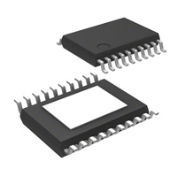
PWP PACKAGE
(TOP VIEW)
BO_OUTZ
OUT1
OUT2
OUT3
OUT4
OUT5
OUT6
OUT7
OUT8
GND
1
2
3
4
5
6
7
8
9
10
20
19
18
17
16
15
14
13
12
11
BO
VIN
5VOUT
SCLK
NCS
MOSI
RST
RDELAY
EN1
NC
NC – No internal connection
DESCRIPTION/ORDERING INFORMATION
The power supply provides regulated 5-V output to power the system microcontroller and drive eight low-side
switches. The brown-out detection output (BO_OUTZ) warns the system if there is a temporary drop in the
supply voltage, so the system can prevent potentially hazardous situations.
A serial communications interface controls the eight low-side outputs; each output has an internal snubber circuit
to absorb the inductive load at turn OFF. Alternatively, the system can use a fly-back diode to VIN to help
recirculate the energy in an inductive load at turn OFF.
ORDERING INFORMATION (1)
TA
–40°C to 125°C
(1)
(2)
PACKAGE (2)
PowerPAD™ – PWP
ORDERABLE PART NUMBER
Reel of 2000
TPL9202PWPR
Tube of 70
TPL9202PWP
TOP-SIDE MARKING
PL202
For the most current package and ordering information, see the Package Option Addendum at the end of this document, or see the TI
web site at www.ti.com.
Package drawings, thermal data, and symbolization are available at www.ti.com/packaging.
1
2
Please be aware that an important notice concerning availability, standard warranty, and use in critical applications of
Texas Instruments semiconductor products and disclaimers thereto appears at the end of this data sheet.
PowerPAD is a trademark of Texas Instruments.
PRODUCTION DATA information is current as of publication date.
Products conform to specifications per the terms of the Texas
Instruments standard warranty. Production processing does not
necessarily include testing of all parameters.
Copyright © 2006–2008, Texas Instruments Incorporated
�TPL9202
8-CHANNEL RELAY DRIVER
WITH INTEGRATED 5-V LDO AND BROWN-OUT DETECTION
www.ti.com
SLIS124D – JUNE 2006 – REVISED FEBRUARY 2008
PINOUT CONFIGURATION
(1)
2
NO.
NAME
I/O
1
BO_OUTZ
O
Brown-out indicator
DESCRIPTION
2
OUT1
O
Low-side output 1
3
OUT2
O
Low-side output 2
4
OUT3
O
Low-side output 3
5
OUT4
O
Low-side output 4
6
OUT5
O
Low-side output 5
7
OUT6
O
Low-side output 6
8
OUT7
O
Low-side output 7
9
OUT8
O
Low-side output 8
10
GND
I
Ground
11
NC
12
EN1
No connection
I
Enable/disable for OUT1
13
RDELAY
O
Power-up reset delay
14 (1)
RST
I/O
Power-on reset output (open drain)
15
MOSI
I
Serial data input
16
NCS
I
Chip select
17
SCLK
I
Serial clock for data synchronization
18
5VOUT
O
Regulated output
19
VIN
I
Unregulated input voltage source
20
BO
I
Brown-out input threshold setting
Terminal 14 can be used as an input or an output.
Submit Documentation Feedback
Copyright © 2006–2008, Texas Instruments Incorporated
Product Folder Link(s): TPL9202
�TPL9202
8-CHANNEL RELAY DRIVER
WITH INTEGRATED 5-V LDO AND BROWN-OUT DETECTION
www.ti.com
SLIS124D – JUNE 2006 – REVISED FEBRUARY 2008
FUNCTIONAL BLOCK DIAGRAM
OUT1
EN1
OUT1
Enables
OUT1
EN1
50 kΩ
OUT1 at
150 mA
6V
Gate Control
for Outputs
1 Through 8
100 kΩ
OUT2
OUT2
OUT2 at 150 mA
OUT3
OUT3 at 150 mA
NCS
OUT3
OUT4
NCS
OUT4 at 150 mA
Parallel
Register
OUT4
OUT5
OUT5 at 150 mA
OUT5
OUT6
OUT6 at 150 mA
SCLK
SCLK
100 kΩ
MOSI
OUT6
OUT7
Serial
Register
OUT7 at 150 mA
OUT7
OUT8
OUT8 at 150 mA
MOSI
20 Ω
(2 W)10 V VIN
OUT8
100 kΩ
7–18 V
PMOS
Optional, dependent
on heat-management
implementation
(see Note A)
5VOUT
Gate Drive
and Control
Bandgap
Ref
Comp
5V
–
GND
+
GND
Vref
5 kΩ
Vref
Voltage
Supervisor
RST
RST
Iconst
RDELAY
RDELAY
BO
VIN
Comp
BO_OUTZ
1.2 V
BO_OUTZ
Recommended
A.
The resistor and Zener diode are required if there is insufficient thermal-management allocation.
Submit Documentation Feedback
Copyright © 2006–2008, Texas Instruments Incorporated
Product Folder Link(s): TPL9202
3
�TPL9202
8-CHANNEL RELAY DRIVER
WITH INTEGRATED 5-V LDO AND BROWN-OUT DETECTION
SLIS124D – JUNE 2006 – REVISED FEBRUARY 2008
www.ti.com
DETAILED DESCRIPTION
The 5-V regulator is powered from VIN, and the regulated output is within 5 V ± 5% over the operating conditions.
The open-drain power-on reset (RST) pin remains low until the regulator exceeds the set threshold, and the timer
value set by the capacitor on the reset delay (RDELAY) pin expires. If both of these conditions are satisfied, RST is
asserted high. This signifies to the microcontroller that serial communications can be initiated to the TPL9202.
The serial communications is an 8-bit format, with data transfer synchronized using a serial clock from the
microcontroller. A single register controls all the outputs (one bit per output). The default value is zero (OFF). If
an output requires pulse width modulation (PWM) function, the register must be updated at a rate faster than the
desired PWM frequency. OUT1 can be controlled by serial input from the microcontroller or with the dedicated
enable (EN1) pin. If EN1 is pulled low or left open, the serial input through the shift register controls OUT1. If
EN1 is pulled high, OUT1 always is turned on, and the serial input for OUT1 is ignored.
The brown-out (BO) input is a resistor divided from the input supply and is used to determine if the supply
voltage drops to undesired levels. If the input drops below the programmed value, BO_OUTZ is pulled low, and
all outputs are disabled. Once the input supply line returns to the minimum desired level, the outputs are enabled
to the previous programmed states.
If RST is asserted, all outputs are turned OFF internally, and the input register is reset to all zeroes. The
microcontroller must write to the register to turn the outputs ON again.
4
Submit Documentation Feedback
Copyright © 2006–2008, Texas Instruments Incorporated
Product Folder Link(s): TPL9202
�TPL9202
8-CHANNEL RELAY DRIVER
WITH INTEGRATED 5-V LDO AND BROWN-OUT DETECTION
www.ti.com
SLIS124D – JUNE 2006 – REVISED FEBRUARY 2008
Absolute Maximum Ratings (1)
MIN
(3)
MAX
UNIT
VIN
24
BO
24
VI(unreg)
Unregulated input voltage (2)
VI(logic)
Logic input voltage (2)
VO
Low-side output voltage
OUT1–OUT8
16.5
V
ILIMIT
Output current limit (4)
OUTn = ON and shorted to VIN
with low impedance
350
mA
θJA
Thermal impedance, junction to ambient (5)
33
°C/W
θJC
Thermal impedance, junction to top of package (5)
20
°C/W
θJP
Thermal impedance, junction to thermal pad (5)
1.4
°C/W
(3)
Continuous power dissipation
ESD
Electrostatic discharge (7)
TA
Operating ambient temperature range
Tstg
Storage temperature range
Tlead
Lead temperature
(2)
(3)
(4)
(5)
(6)
(7)
7
RST and RDELAY
7
(6)
PD
(1)
EN1, MOSI, SCLK, and NCS
V
V
3.7
W
2
kV
–40
125
°C
–65
125
°C
260
°C
Soldering, 10 s
Stresses beyond those listed under "absolute maximum ratings" may cause permanent damage to the device. These are stress ratings
only and functional operation of the device at these or any other conditions beyond those indicated under "recommended operating
conditions" is not implied. Exposure to absolute-maximum-rated conditions for extended periods may affect device reliability.
All voltage values are with respect to GND.
Absolute negative voltage on these pins must not go below –0.5 V.
Not more than one output should be shorted at a time, and duration of the short circuit should not exceed 1 ms.
The thermal data is based on using 1-oz copper trace with JEDEC 51-5 test board for PWP.
The data is based on ambient temperature of 25°C maximum.
The Human Body Model is a 100-pF capacitor discharged through a 1.5-kΩ resistor into each pin.
Dissipation Ratings
PACKAGE
TA ≤ 25°C
POWER RATING
DERATING FACTOR
ABOVE TA = 25°C
TA = 125°C
POWER RATING
PWP
3787 mW
30.3 mW/°C
757 mW
Recommended Operating Conditions
VI(unreg)
Unregulated input voltage
VI(logic)
Logic input voltage
TA
Operating ambient temperature
MIN
MAX
VIN
7
18
BO (as seen by external resistor network)
0
18
0
5.25
V
–40
125
°C
EN1, RST, and RDELAY , MOSI, SCLK, and NCS
Submit Documentation Feedback
Copyright © 2006–2008, Texas Instruments Incorporated
Product Folder Link(s): TPL9202
UNIT
V
5
�TPL9202
8-CHANNEL RELAY DRIVER
WITH INTEGRATED 5-V LDO AND BROWN-OUT DETECTION
www.ti.com
SLIS124D – JUNE 2006 – REVISED FEBRUARY 2008
Electrical Characteristics
TA = –40°C to 125°C, VIN = 7 V to 18 V (unless otherwise noted)
PARAMETER
MIN TYP (1)
TEST CONDITIONS
MAX
UNIT
Supply Voltage and Current
VIN (2)
Input voltage
IIN
Input supply current
7
18
Enable = low, OUT1–OUT8 = Off
3
Enable = high, OUT1–OUT8 = On
5
V
mA
Logic Inputs (MOSI, NCS, SCLK, and EN1)
VIL
Logic input low level
IIL = 100 µA
VIH
Logic input high level
IIL = 100 µA
VOL
Low-level logic output
IOL = 1.6 mA
VOH (3)
High-level logic output
5-kΩ pullup to VCC
VH
Disabling reset threshold
5-V regulator ramps up
VL
Enabling reset threshold
5-V regulator ramps down
VHYS
Threshold hysteresis
0.8
2.4
V
V
Reset (RST)
0.4
VCC – 0.8
V
V
4.25
4.5
V
3.3
3.75
V
0.12
0.5
V
18
28
Reset Delay (RDELAY)
Output current
tDW
Reset delay timer
C = 47 nF
6
ms
tUP
Reset capacitor to low level
C = 47 nF
45
µs
0.4
3
48
µA
IOUT
Output (OUT1–OUT8)
VOL
Output ON
IOUTn = 150 mA
IOH
Output leakage
VOH = Max of 16.5 V
0.7
V
2
µA
5.25
V
Regulator Output (5VOUT)
5VOUT
Output supply
I5VOUT = 5 mA to 200 mA, VIN = 7 V to 18 V,
C5VOUT = 1 µF
4.75
I5Vout
Limit output short circuit
current
5VOUT = 0 V
200
5
mA
Brown-Out (BO) Input
BOVthes
Threshold for brown-out
detection
VIN reduced until BO_OUTZ goes low
1.3
V
Brown-Out Detection Output (BO_OUTZ)
VOL
Logic level output
IOL = 100 µA
VOH (3)
Logic level output
Pullup to VCC
0.4
VCC – 0.8
V
V
Thermal Shutdown
TSD
Thermal shutdown
THYS
Hysteresis
(1)
(2)
(3)
6
150
°C
20
°C
All typical values are at TA = 25°C.
There are external high-frequency noise-suppression capacitors and filter capacitors on VIN.
VCC is the pullup resistor voltage.
Submit Documentation Feedback
Copyright © 2006–2008, Texas Instruments Incorporated
Product Folder Link(s): TPL9202
�TPL9202
8-CHANNEL RELAY DRIVER
WITH INTEGRATED 5-V LDO AND BROWN-OUT DETECTION
www.ti.com
SLIS124D – JUNE 2006 – REVISED FEBRUARY 2008
Output Control Register
MSB
LSB
IN8
IN7
IN6
IN5
IN4
IN3
IN2
IN1
0
0
0
0
0
0
0
0
INn = 0 = Output OFF
INn = 1 = Output ON
To operate the output in PWM mode, the output control register must be updated at a rate twice the desired
PWM frequency of the output. Maximum PWM frequency is 5 kHz. The register is updated every 100 µs.
ENABLE TRUTH TABLE
EN1
SERIAL INPUT
FOR OUT1
OUT1
Open
H
On
Open
L
Off
L
H
On
L
L
Off
H
H
On
H
L
On
Submit Documentation Feedback
Copyright © 2006–2008, Texas Instruments Incorporated
Product Folder Link(s): TPL9202
7
�TPL9202
8-CHANNEL RELAY DRIVER
WITH INTEGRATED 5-V LDO AND BROWN-OUT DETECTION
www.ti.com
SLIS124D – JUNE 2006 – REVISED FEBRUARY 2008
Serial Communications Interface
The serial communications are an 8-bit format, with data transfer synchronized using a serial clock from the
microcontroller (see Figure 1). A single register controls all the outputs. The signal gives the instruction to control
the output of TPL9202.
The NCS signal enables the SCLK and MOSI data when it is low. After NCS is set to low for T1, synchronization
clock and data begin to transmit and, after the 8-bit data has been transmitted, NCS is set high again to disable
SCLK and MOSI and to transfer the serial data to the control register. SCLK must be held low when NCS is high.
T2
T3
T8
T1
T4
T5
T1
NCS
SCLK
1
2
3
4
5
6
7
8
LSB
MSB
MOSI
XXX
IN8
IN7
IN6
IN5
IN4
IN3
IN1
IN2
T6
T7
Figure 1. Serial Communications
8
Submit Documentation Feedback
Copyright © 2006–2008, Texas Instruments Incorporated
Product Folder Link(s): TPL9202
�www.ti.com
TPL9202
8-CHANNEL RELAY DRIVER
WITH INTEGRATED 5-V LDO AND BROWN-OUT DETECTION
SLIS124D – JUNE 2006 – REVISED FEBRUARY 2008
Timing Requirements
TA = –40°C to 125°C, VIN = 7 V to 18 V (unless otherwise noted)
MIN
TYP
MAX
4
UNIT
fSPI
SPI frequency
T1
Delay time, NCS falling edge to SCLK rising edge
10
MHz
ns
T2
Delay time, NCS falling edge to SCLK falling edge
80
ns
T3
Pulse duration, SCLK high
60
ns
T4
Pulse duration, SCLK low
60
ns
T5
Delay time, last SCLK falling edge to NCS rising edge
80
ns
T6
Setup time, MOSI valid before SCLK edge
10
ns
T7
Hold time, MOSI valid after SCLK edge
10
ns
T8
Time between two words for transmitting
170
ns
Reset Delay (RDELAY)
The RDELAY output provides a constant current source to charge an external capacitor to approximately 6.5 V.
The external capacitor is selected to provide a delay time, based on the current equation for a capacitor,
I = C(Δv/Δt) and a 28-µA typical output current.
Therefore, the user should select a 47-nF capacitor to provide a 6-ms delay at 3.55 V.
I = C(Δv/Δt)
28 µA = C × (3.55 V/6 ms)
C = 47 nF
Submit Documentation Feedback
Copyright © 2006–2008, Texas Instruments Incorporated
Product Folder Link(s): TPL9202
9
�TPL9202
8-CHANNEL RELAY DRIVER
WITH INTEGRATED 5-V LDO AND BROWN-OUT DETECTION
www.ti.com
SLIS124D – JUNE 2006 – REVISED FEBRUARY 2008
APPLICATION INFORMATION
Buzzer Driver
Relay Driver
Relay Driver
Relay Driver
Relay Driver
Fan Driver
Fan Driver
Fan Driver
MOSI
SCLK
MCU/DSP
NCS
8 Outputs
BO_OUTZ
TPL9202
RST
5VOUT ±5% at 200 mA
Brown Out
EN1
RDELAY
DC Input 7 V to 18 V
GND
Figure 2. Typical Application
Display
(LED/LCD/VFD)
AC
Filters
Keypad
LED LED
Water
Supply
Valve
Water
Outlet
Softener
Supply
Volume
Sensor
M
Power
Switch
Controller
Water-Level
Sensor
Driver
BO
VIN
+
~
Optical
Sensor
BO_OUTZ
Brown-Out
Detect
Regulator
~
Temperature
Sensor
(Optional)
5VOUT
POR/SYS
RST
-
Cover
Switch
TPL9202
Figure 3. Washing-Machine Application
10
Submit Documentation Feedback
Copyright © 2006–2008, Texas Instruments Incorporated
Product Folder Link(s): TPL9202
�TPL9202
8-CHANNEL RELAY DRIVER
WITH INTEGRATED 5-V LDO AND BROWN-OUT DETECTION
www.ti.com
SLIS124D – JUNE 2006 – REVISED FEBRUARY 2008
PCB Layout
To maximize the efficiency of this package for application on a single layer or multilayer PCB, certain guidelines
must be followed when laying out this part on the PCB.
The following information is to be used as a guideline only.
For further information, see the PowerPAD concept implementation document.
Application Using a Multilayer PCB
In a multilayer board application, the thermal vias are the primary method of heat transfer from the package
thermal pad to the internal ground plane (see Figure 4 and Figure 5).
The efficiency of this method depends on several factors: die area, number of thermal vias, thickness of copper,
etc. (see the PowerPAD™ Thermally Enhanced Package Technical Brief, literature number SLMA002).
Solder Pad (Land Pattern)
Package Thermal Pad
Thermal Vias
Package Outline
Figure 4. Package and PCB Land Configuration for a Multilayer PCB
Power Pad
Package Solder Pad
Component Traces
1.5038–1.5748-mm
Component Trace
(2-oz Cu)
2 Plane
4 Plane
Thermal Via
1.5748 mm
Thermal Isolation
Power Plane Only
1.0142–1.0502-mm
Ground Plane
(1-oz Cu)
0.5246–0.5606-mm
Power Plane
(1-oz Cu)
0.0–0.071-mm Board Base
and Bottom Pad
Package Solder Pad
(Bottom Trace)
Figure 5. Multilayer Board (Side View)
Application Using a Single-Layer PCB
In a single-layer board application, the thermal pad is attached to a heat spreader (copper areas) by a low
thermal-impedance attachment method (solder paste or thermal conductive epoxy). With either method, it is
advisable to use as many copper traces as possible to dissipate the heat.
Submit Documentation Feedback
Copyright © 2006–2008, Texas Instruments Incorporated
Product Folder Link(s): TPL9202
11
�TPL9202
8-CHANNEL RELAY DRIVER
WITH INTEGRATED 5-V LDO AND BROWN-OUT DETECTION
www.ti.com
SLIS124D – JUNE 2006 – REVISED FEBRUARY 2008
CAUTION:
If the attachment method is not implemented correctly, the functionality of the
product cannot be ensured. Power-dissipation capability is adversely affected if
the device is incorrectly mounted on the circuit board.
Use as Much Copper Area
as Possible for Heat Spread
Package Thermal Pad
Package Outline
Figure 6. Layout Recommendations for a Single-Layer PCB
12
Submit Documentation Feedback
Copyright © 2006–2008, Texas Instruments Incorporated
Product Folder Link(s): TPL9202
�TPL9202
8-CHANNEL RELAY DRIVER
WITH INTEGRATED 5-V LDO AND BROWN-OUT DETECTION
www.ti.com
SLIS124D – JUNE 2006 – REVISED FEBRUARY 2008
Recommended Board Layout
6,5 SMOC
5,85
SMOC = Solder Mask Over Copper
SMO = Solder Mask Opening
8)
3 (´
1
2,4 SMO
3,4 SMOC
4,52
6,92
0,3
1,2 (´20)
1
0,65
0,27 (´20)
3,7 SMO
Figure 7. Recommended Board Layout for PWP
Submit Documentation Feedback
Copyright © 2006–2008, Texas Instruments Incorporated
Product Folder Link(s): TPL9202
13
�PACKAGE OPTION ADDENDUM
www.ti.com
14-Oct-2022
PACKAGING INFORMATION
Orderable Device
Status
(1)
Package Type Package Pins Package
Drawing
Qty
Eco Plan
(2)
Lead finish/
Ball material
MSL Peak Temp
Op Temp (°C)
Device Marking
(3)
Samples
(4/5)
(6)
TPL9202PWP
ACTIVE
HTSSOP
PWP
20
70
RoHS & Green
NIPDAU
Level-2-260C-1 YEAR
-40 to 125
PL202
Samples
TPL9202PWPR
ACTIVE
HTSSOP
PWP
20
2000
RoHS & Green
NIPDAU
Level-2-260C-1 YEAR
-40 to 125
PL202
Samples
(1)
The marketing status values are defined as follows:
ACTIVE: Product device recommended for new designs.
LIFEBUY: TI has announced that the device will be discontinued, and a lifetime-buy period is in effect.
NRND: Not recommended for new designs. Device is in production to support existing customers, but TI does not recommend using this part in a new design.
PREVIEW: Device has been announced but is not in production. Samples may or may not be available.
OBSOLETE: TI has discontinued the production of the device.
(2)
RoHS: TI defines "RoHS" to mean semiconductor products that are compliant with the current EU RoHS requirements for all 10 RoHS substances, including the requirement that RoHS substance
do not exceed 0.1% by weight in homogeneous materials. Where designed to be soldered at high temperatures, "RoHS" products are suitable for use in specified lead-free processes. TI may
reference these types of products as "Pb-Free".
RoHS Exempt: TI defines "RoHS Exempt" to mean products that contain lead but are compliant with EU RoHS pursuant to a specific EU RoHS exemption.
Green: TI defines "Green" to mean the content of Chlorine (Cl) and Bromine (Br) based flame retardants meet JS709B low halogen requirements of


 工商网监
湘ICP备2023018690号
工商网监
湘ICP备2023018690号
