TPS2010A, TPS2011A
TPS2012A, TPS2013A
www.ti.com
SLVS189C – DECEMBER 1998 – REVISED SEPTEMBER 2007
POWER-DISTRIBUTION SWITCHES
FEATURES
1
•
•
•
•
•
•
•
•
•
•
•
33-mΩ (5-V Input) High-Side MOSFET Switch
Short-Circuit and Thermal Protection
Operating Range . . . 2.7 V to 5.5 V
Logic-Level Enable Input
Typical Rise Time. . . 6.1 ms
Undervoltage Lockout
Maximum Standby Supply Current. . . 10 μA
No Drain-Source Back-Gate Diode
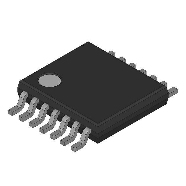
Available in 8-pin SOIC and 14-Pin TSSOP
Packages
Ambient Temperature Range, –40°C to 85°C
2-kV Human-Body-Model, 200-V
Machine-Model ESD Protection
DESCRIPTION
The TPS201xA family of power distribution switches is intended for applications where heavy capacitive loads
and short circuits are likely to be encountered. These devices are 50-mΩ N-channel MOSFET high-side power
switches. The switch is controlled by a logic enable compatible with 5-V logic and 3-V logic. Gate drive is
provided by an internal charge pump designed to control the power-switch rise times and fall times to minimize
current surges during switching. The charge pump requires no external components and allows operation from
supplies as low as 2.7 V.
When the output load exceeds the current-limit threshold or a short is present, the TPS201xA limits the output
current to a safe level by switching into a constant-current mode. When continuous heavy overloads and short
circuits increase the power dissipation in the switch, causing the junction temperature to rise, a thermal
protection circuit shuts off the switch to prevent damage. Recovery from a thermal shutdown is automatic once
the device has cooled sufficiently. Internal circuitry ensures the switch remains off until valid input voltage is
present.
TPS201xA
TPS202x
TPS203x
0.2 A - 2 A
0.2 A - 2 A
0.2 A - 2 A
TPS2014
TPS2015
TPS2041B
TPS2051B
TPS2045A
TPS2049
TPS2055A
TPS2061
TPS2065
TPS2068
TPS2069
600 mA
1A
500 mA
500 mA
250 mA
100 mA
250 mA
1A
1A
1.5 A
1.5 A
1
Please be aware that an important notice concerning availability, standard warranty, and use in critical applications of
Texas Instruments semiconductor products and disclaimers thereto appears at the end of this data sheet.
PRODUCTION DATA information is current as of publication date.
Products conform to specifications per the terms of the Texas
Instruments standard warranty. Production processing does not
necessarily include testing of all parameters.
Copyright © 1998–2007, Texas Instruments Incorporated
�TPS2010A, TPS2011A
TPS2012A, TPS2013A
www.ti.com
SLVS189C – DECEMBER 1998 – REVISED SEPTEMBER 2007
These devices have limited built-in ESD protection. The leads should be shorted together or the device placed in conductive foam
during storage or handling to prevent electrostatic damage to the MOS gates.
DESCRIPTION (CONTINUED)
The TPS201xA devices differ only in short-circuit current threshold. The TPS2010A limits at 0.3-A load, the
TPS2011 at 0.9-A load, the TPS2012A at 1.5-A load, and the TPS2013A at 2.2-A load (see Available Options).
The TPS201xA is available in an 8-pin small-outline integrated-circuit (SOIC) package and in a 14-pin thin-shrink
small-outline package (TSSOP) and operates over a junction temperature range of -40°C to 125°C.)
AVAILABLE OPTIONS
TA
ENABLE
–40°C to 85°C
(1)
(2)
(3)
PACKAGED DEVICES (1)
RECOMMENDED
MAXIMUM CONTINUOUS
LOAD CURRENT
(A)
TYPICAL SHORT-CIRCUIT
CURRENT LIMIT AT 25°C
(A)
SMALL OUTLINE
(D) (2)
TSSOP
(PWP) (3)
0.2
0.3
TPS2010AD
TPS2010APWPR
0.6
0.9
TPS2011AD
TPS2011APWPR
1
1.5
TPS2012AD
TPS2012APWPR
1.5
2.2
TPS2013AD
TPS2013APWPR
Active low
For the most current package and ordering information, see the Package Option Addendum at the end of this document, or see the TI
website at www.ti.com.
The D package is available taped and reeled. Add an R suffix to device type (e.g., TPS2010DR)
The PWP package is only available left-end taped-and-reeled.
TPS201xA FUNCTIONAL BLOCK DIAGRAM
TERMINAL FUNCTIONS
TERMINAL
NAME
NO.
I/O
DESCRIPTION
D
PWP
EN
4
7
I
Enable input. Logic low turns on power switch.
GND
1
1
I
Ground
IN
2, 3
2–6
I
Input voltage
OUT
5–8
8–14
O
Power-switch output
2
Submit Documentation Feedback
Copyright © 1998–2007, Texas Instruments Incorporated
Product Folder Link(s): TPS2010A, TPS2011A TPS2012A, TPS2013A
�TPS2010A, TPS2011A
TPS2012A, TPS2013A
www.ti.com
SLVS189C – DECEMBER 1998 – REVISED SEPTEMBER 2007
DETAILED DESCRIPTION
POWER SWITCH
The power switch is an N-channel MOSFET with a maximum on-state resistance of 50 mΩ (VI(IN) = 5V).
Configured as a high-side switch, the power switch prevents current flow from OUT to IN and IN to OUT when
disabled.
CHARGE PUMP
An internal charge pump supplies power to the driver circuit and provides the necessary voltage to pull the gate
of the MOSFET above the source. The charge pump operates from input voltages as low as 2.7 V and requires
very little supply current.
DRIVER
The driver controls the gate voltage of the power switch. To limit large current surges and reduce the associated
electromagnetic interference (EMI) produced, the driver incorporates circuitry that controls the rise times and fall
times of the output voltage. The rise and fall times are typically in the 2-ms to 9-ms range.
ENABLE (EN)
The logic enable disables the power switch, the bias for the charge pump, driver, and other circuitry to reduce the
supply current to less than 10 μA when a logic high is present on EN . A logic zero input on EN restores bias to
the drive and control circuits and turns the power on. The enable input is compatible with both TTL and CMOS
logic levels.
CURRENT SENSE
A sense FET monitors the current supplied to the load. The sense FET measures current more efficiently than
conventional resistance methods. When an overload or short circuit is encountered, the current-sense circuitry
sends a control signal to the driver. The driver, in turn, reduces the gate voltage and drives the power FET into
its saturation region, which switches the output into a constant current mode and holds the current constant while
varying the voltage on the load.
THERMAL SENSE
An internal thermal-sense circuit shuts off the power switch when the junction temperature rises to approximately
140°C. Hysteresis is built into the thermal sense circuit. After the device has cooled approximately 20°C, the
switch turns back on. The switch continues to cycle off and on until the fault is removed.
UNDERVOLTAGE LOCKOUT
A voltage sense circuit monitors the input voltage. When the input voltage is below approximately 2 V, a control
signal turns off the power switch.
Copyright © 1998–2007, Texas Instruments Incorporated
Submit Documentation Feedback
Product Folder Link(s): TPS2010A, TPS2011A TPS2012A, TPS2013A
3
�TPS2010A, TPS2011A
TPS2012A, TPS2013A
www.ti.com
SLVS189C – DECEMBER 1998 – REVISED SEPTEMBER 2007
ABSOLUTE MAXIMUM RATINGS
over operating free-air temperature range (unless otherwise noted) (1)
VI(IN)
Input voltage range (2)
VO(OUT)
Output voltage range (2)
VI(EN)
Input voltage range
IO(OUT)
Continuous output current
VALUE
UNIT
–0.3 to 6
V
–0.3 to VI(IN) + 0.3
V
–0.3 to 6
V
Internally Limited
Continuous total power dissipation
See Dissipation Rating Table
TJ
Operating virtual junction temperature range
–40 to 125
°C
Tstg
Storage temperature range
–65 to 150
°C
260
°C
2
kV
200
V
Lead temperature soldering 1,6 mm (1/16 inch) from case for 10 seconds
ESD
(1)
(2)
Electrostatic discharge protection
Human body model
Machine model
Stresses beyond those listed under absolute maximum ratings may cause permanent damage to the device. These are stress ratings
only, and functional operation of the device at these or any other conditions beyond those indicated under recommended operating
conditions is not implied. Exposure to absolute-maximum-rated conditions for extended periods may affect device reliability.
All voltages are with respect to GND.
DISSIPATION RATINGS
PACKAGE
TA ≤ 25°C
POWER RATING
DERATING FACTOR
ABOVE TA = 25°C
TA = 70°C
POWER RATING
TA = 85°C
POWER RATING
D
725 mW
5.8 mW/°C
464 mW
377 mW
PWP
700 mW
5.6 mW/°C
448 mW
364 mW
RECOMMENDED OPERATING CONDITIONS
over operating free-air temperature range (unless otherwise noted)
VI(IN)
VIH
MIN
MAX
2.7
5.5
0
5.5
TPS2010A
0
0.2
TPS2011A
0
0.6
TPS2012A
0
1
Input voltage
IO
Continuous output current
TJ
Operating virtual junction temperature
TPS2013A
4
Submit Documentation Feedback
0
1.5
–40
125
UNIT
V
A
°C
Copyright © 1998–2007, Texas Instruments Incorporated
Product Folder Link(s): TPS2010A, TPS2011A TPS2012A, TPS2013A
�TPS2010A, TPS2011A
TPS2012A, TPS2013A
www.ti.com
SLVS189C – DECEMBER 1998 – REVISED SEPTEMBER 2007
ELECTRICAL CHARACTERISTICS
over recommended operating junction temperature range, VI(IN) = 5.5 V, IO = rated current, EN = 0 V (unless otherwise noted)
TEST CONDITIONS (1)
PARAMETER
MIN
TYP
MAX
UNIT
POWER SWITCH
rDS(on)
Static drain-source on-state
resistance
tr
Rise time, output
tf
Rise time, output
VI(IN) = 5 V,
TJ = 25°C,
IO = 1.5 A
33
36
VI(IN) = 5 V,
TJ = 85°C,
IO = 1.5 A
38
46
VI(IN) = 5 V,
TJ = 125°C,
IO = 1.5 A
44
50
VI(IN) = 3.3 V,
TJ = 25°C,
IO = 1.5 A
37
41
VI(IN) = 3.3 V,
TJ = 85°C,
IO = 1.5 A
43
52
VI(IN) = 3.3 V,
TJ = 125°C,
IO = 1.5 A
51
61
VI(IN) = 5 V,
TJ = 25°C,
IO = 0.18 A
30
34
VI(IN) = 5 V,
TJ = 85°C,
IO = 0.18 A
35
41
VI(IN) = 5 V,
TJ = 125°C,
IO = 0.18 A
39
47
VI(IN) = 3.3 V,
TJ = 25°C,
IO = 0.18 A
33
37
VI(IN) = 3.3 V,
TJ = 85°C,
IO = 0.18 A
39
46
VI(IN) = 3.3 V,
TJ = 125°C,
IO = 0.18 A
44
56
VI(IN) = 5.5 V,
TJ = 25°C,
CL = 1 μF,
RL = 10 Ω
6.1
VI(IN) = 2.7 V,
TJ = 25°C,
CL = 1 μF,
RL = 10 Ω
8.6
VI(IN) = 5.5 V,
TJ = 25°C,
CL = 1 μF,
RL = 10 Ω
3.4
VI(IN) = 2.7 V,
TJ = 25°C,
CL = 1 μF,
RL = 10 Ω
3
TPS2013A
TPS2010A
mΩ
mΩ
ms
ms
ENABLE INPUT (EN)
VIH
2.7 V ≤ VI(IN) ≤ 5.5 V
High-level input voltage
2
V
4.5 V ≤ VI(IN) ≤ 5.5 V
0.8
2.7 V ≤ VI(IN) ≤ 4.5 V
0.5
VIL
Low-level input voltage
II
Input current
EN = 0 V or EN = VI(IN)
ton
Turnon time
CL = 100 μF,
toff
Turnoff time
CL = 100 μF,
V
0.5
μA
RL = 10 Ω
20
ms
RL = 10 Ω
40
ms
–0.5
CURRENT LIMIT
IOS
(1)
Short-circuit output current
TJ = 25°C, VI = 5.5 V,
OUT connected to GND,
Device enable into short circuit
TPS2010A
0.22
0.3
0.4
TPS2011A
0.66
0.9
1.1
TPS2012A
1.1
1.5
1.8
TPS2013A
1.65
2.2
2.7
A
Pulse-testing techniques maintain junction temperature close to ambient temperature; thermal effects must be taken into account
separately.
Copyright © 1998–2007, Texas Instruments Incorporated
Submit Documentation Feedback
Product Folder Link(s): TPS2010A, TPS2011A TPS2012A, TPS2013A
5
�TPS2010A, TPS2011A
TPS2012A, TPS2013A
www.ti.com
SLVS189C – DECEMBER 1998 – REVISED SEPTEMBER 2007
ELECTRICAL CHARACTERISTICS (Continued)
over recommended operating junction temperature range, VI(IN) = 5.5 V, IO = rated current, EN = 0 V (unless otherwise noted)
TEST CONDITIONS (1)
PARAMETER
MIN
TYP MAX
UNIT
SUPPLY CURRENT
Supply current, low-level output
No Load on OUT
EN = VI(IN)
Supply current, high-level output
No Load on OUT
EN = 0 V
Leakage current
OUT connected to ground
EN = VI(IN)
TJ = 25°C
0.3
–40°C ≤ TJ ≤ 125°C
1
10
TJ = 25°C
58
75
–40°C ≤ TJ ≤ 125°C
75
100
–40°C ≤ TJ ≤ 125°C
10
μA
μA
μA
UNDERVOLTAGE LOCKOUT
Low-level input voltage
Hysteresis
(1)
6
2
TJ = 25°C
2.5
100
V
mV
Pulse-testing techniques maintain junction temperature close to ambient temperature; thermal effects must be taken into account
separately.
Submit Documentation Feedback
Copyright © 1998–2007, Texas Instruments Incorporated
Product Folder Link(s): TPS2010A, TPS2011A TPS2012A, TPS2013A
�TPS2010A, TPS2011A
TPS2012A, TPS2013A
www.ti.com
SLVS189C – DECEMBER 1998 – REVISED SEPTEMBER 2007
PARAMETER MEASUREMENT INFORMATION
Figure 1. Test Circuit and Voltage Waveforms
Table 1. Timing Diagrams
FIGURE
Turnon Delay and Rise Time
2
Turnoff Delay and Fall Time
3
Turnon Delay and Rise TIME with 1-μF Load
4
Turnoff Delay and Rise TIME with 1-μF Load
5
Device Enabled into Short
6
TPS2010A, TPS2011A, TPS2012A, and TPS2013A, Ramped Load on Enabled Device
7, 8, 9, 10
TPS2013A, Inrush Current
11
7.9-Ω Load Connected to an Enabled TPS2010A Device
12
3.7-Ω Load Connected to an Enabled TPS2010A Device
13
3.7-Ω Load Connected to an Enabled TPS2011A Device
14
2.6-Ω Load Connected to an Enabled TPS2011A Device
15
2.6-Ω Load Connected to an Enabled TPS2012A Device
16
1.2-Ω Load Connected to an Enabled TPS2012A Device
17
1.2-Ω Load Connected to an Enabled TPS2013A Device
18
0.9-Ω Load Connected to an Enabled TPS2013A Device
19
Copyright © 1998–2007, Texas Instruments Incorporated
Submit Documentation Feedback
Product Folder Link(s): TPS2010A, TPS2011A TPS2012A, TPS2013A
7
�TPS2010A, TPS2011A
TPS2012A, TPS2013A
www.ti.com
SLVS189C – DECEMBER 1998 – REVISED SEPTEMBER 2007
8
Figure 2. Turnon Delay and Rise Time
Figure 3. Turnoff Delay and Fall Time
Figure 4. Turnon Delay and Rise Time With 1-μF Load
Figure 5. Turnoff Delay and Fall Time With 1-μF Load
Submit Documentation Feedback
Copyright © 1998–2007, Texas Instruments Incorporated
Product Folder Link(s): TPS2010A, TPS2011A TPS2012A, TPS2013A
�TPS2010A, TPS2011A
TPS2012A, TPS2013A
www.ti.com
SLVS189C – DECEMBER 1998 – REVISED SEPTEMBER 2007
Figure 6. Device Enabled Into Short
Figure 7. TPS2010A, Ramped Load on Enabled Device
Figure 8. TPS2011A, Ramped Load on Enabled Device
Figure 9. TPS2012A, Ramped Load on Enabled Device
Copyright © 1998–2007, Texas Instruments Incorporated
Submit Documentation Feedback
Product Folder Link(s): TPS2010A, TPS2011A TPS2012A, TPS2013A
9
�TPS2010A, TPS2011A
TPS2012A, TPS2013A
www.ti.com
SLVS189C – DECEMBER 1998 – REVISED SEPTEMBER 2007
10
Figure 10. TPS2013A, Ramped Load on Enabled Device
Figure 11. TPS2013A, Inrush Current
Figure 12. 7.9-Ω Load Connected to an Enabled
TPS2010A Device
Figure 13. 3.7-Ω Load Connected to an Enabled
TPS2010A Device
Submit Documentation Feedback
Copyright © 1998–2007, Texas Instruments Incorporated
Product Folder Link(s): TPS2010A, TPS2011A TPS2012A, TPS2013A
�TPS2010A, TPS2011A
TPS2012A, TPS2013A
www.ti.com
SLVS189C – DECEMBER 1998 – REVISED SEPTEMBER 2007
Figure 14. 3.7-Ω Load Connected to an Enabled
TPS2011A Device
Figure 15. 2.6-Ω Load Connected to an Enabled
TPS2011A Device
Figure 16. 2.6-Ω Load Connected to an Enabled
TPS2012A Device
Figure 17. 1.2-Ω Load Connected to an Enabled
TPS2012A Device
Copyright © 1998–2007, Texas Instruments Incorporated
Submit Documentation Feedback
Product Folder Link(s): TPS2010A, TPS2011A TPS2012A, TPS2013A
11
�TPS2010A, TPS2011A
TPS2012A, TPS2013A
www.ti.com
SLVS189C – DECEMBER 1998 – REVISED SEPTEMBER 2007
Figure 18. 1.2-Ω Load Connected to an Enabled TPS2013A Device
Figure 19. 0.9-Ω Load Connected to an Enabled TPS2013A Device
12
Submit Documentation Feedback
Copyright © 1998–2007, Texas Instruments Incorporated
Product Folder Link(s): TPS2010A, TPS2011A TPS2012A, TPS2013A
�TPS2010A, TPS2011A
TPS2012A, TPS2013A
www.ti.com
SLVS189C – DECEMBER 1998 – REVISED SEPTEMBER 2007
TYPICAL CHARACTERISTICS
Table of Graphs
FIGURE
td(on)
Turnon delay time
vs Output voltage
20
td(off)
Turnoff delay time
vs Input voltage
21
tr
Rise time
vs Load current
22
tf
Fall time
vs Load current
23
Supply current (enabled)
vs Junction temperature
24
Supply current (disabled)
vs Junction temperature
25
Supply current (enabled)
vs Input voltage
26
Supply current (disabled)
vs Input voltage
27
Short-circuit current limit
vs Input voltage
28
vs Junction temperature
29
vs Input voltage
30
vs Junction temperature
31
vs Input voltage
32
vs Junction temperature
33
Input voltage vs Temperature
34
IOS
rDS(on)
Static drain-source on-state resistance
Undervoltage lockout
TURNON DELAY TIME
vs
OUTPUT VOLTAGE
TURNOFF DELAY TIME
vs
INPUT VOLTAGE
Figure 20.
Figure 21.
Copyright © 1998–2007, Texas Instruments Incorporated
Submit Documentation Feedback
Product Folder Link(s): TPS2010A, TPS2011A TPS2012A, TPS2013A
13
�TPS2010A, TPS2011A
TPS2012A, TPS2013A
www.ti.com
SLVS189C – DECEMBER 1998 – REVISED SEPTEMBER 2007
14
RISE TIME
vs
LOAD CURRENT
FALL TIME
vs
LOAD CURRENT
Figure 22.
Figure 23.
SUPPLY CURRENT (ENABLED)
vs
JUNCTION TEMPERATURE
SUPPLY CURRENT (DISABLED)
vs
JUNCTION TEMPERATURE
Figure 24.
Figure 25.
Submit Documentation Feedback
Copyright © 1998–2007, Texas Instruments Incorporated
Product Folder Link(s): TPS2010A, TPS2011A TPS2012A, TPS2013A
�TPS2010A, TPS2011A
TPS2012A, TPS2013A
www.ti.com
SLVS189C – DECEMBER 1998 – REVISED SEPTEMBER 2007
SUPPLY CURRENT (ENABLED)
vs
INPUT VOLTAGE
SUPPLY CURRENT (DISABLED)
vs
INPUT VOLTAGE
Figure 26.
Figure 27.
SHORT-CIRCUIT CURRENT LIMIT
vs
INPUT VOLTAGE
SHORT-CIRCUIT CURRENT LIMIT
vs
JUNCTION TEMPERATURE
Figure 28.
Figure 29.
Copyright © 1998–2007, Texas Instruments Incorporated
Submit Documentation Feedback
Product Folder Link(s): TPS2010A, TPS2011A TPS2012A, TPS2013A
15
�TPS2010A, TPS2011A
TPS2012A, TPS2013A
www.ti.com
SLVS189C – DECEMBER 1998 – REVISED SEPTEMBER 2007
16
STATIC DRAIN-SOURCE ON-STATE RESISTANCE
vs
INPUT VOLTAGE
STATIC DRAIN-SOURCE ON-STATE RESISTANCE
vs
JUNCTION TEMPERATURE
Figure 30.
Figure 31.
STATIC DRAIN-SOURCE ON-STATE RESISTANCE
vs
INPUT VOLTAGE
STATIC DRAIN-SOURCE ON-STATE RESISTANCE
vs
JUNCTION TEMPERATURE
Figure 32.
Figure 33.
Submit Documentation Feedback
Copyright © 1998–2007, Texas Instruments Incorporated
Product Folder Link(s): TPS2010A, TPS2011A TPS2012A, TPS2013A
�TPS2010A, TPS2011A
TPS2012A, TPS2013A
www.ti.com
SLVS189C – DECEMBER 1998 – REVISED SEPTEMBER 2007
UNDERVOLTAGE LOCKOUT
Figure 34.
Copyright © 1998–2007, Texas Instruments Incorporated
Submit Documentation Feedback
Product Folder Link(s): TPS2010A, TPS2011A TPS2012A, TPS2013A
17
�TPS2010A, TPS2011A
TPS2012A, TPS2013A
www.ti.com
SLVS189C – DECEMBER 1998 – REVISED SEPTEMBER 2007
APPLICATION INFORMATION
Figure 35. Typical Application
POWER-SUPPLY CONSIDERATIONS
A 0.01-μF to 0.1-μF ceramic bypass capacitor between IN and GND, close to the device, is recommended.
Placing a high-value electrolytic capacitor on the output and input pins is recommended when the output load is
heavy. This precaution reduces power supply transients that may cause ringing on the input. Additionally,
bypassing the output with a 0.01-μF to 0.1-μF ceramic capacitor improves the immunity of the device to
short-circuit transients.
OVERCURRENT
A sense FET checks for overcurrent conditions. Unlike current-sense resistors, sense FETs do not increase the
series resistance of the current path. When an overcurrent condition is detected, the device maintains a constant
output current and reduces the output voltage accordingly. Complete shutdown occurs only if the fault is present
long enough to activate thermal limiting.
Three possible overload conditions can occur. In the first condition, the output has been shorted before the
device is enabled or before VI(IN) has been applied (see Figure 6). The TPS201xA senses the short and
immediately switches into a constant-current output.
In the second condition, the excessive load occurs while the device is enabled. At the instant the excessive load
occurs, very high currents may flow for a short time before the current-limit circuit can react (see
Figure 12–Figure 19). After the current-limit circuit has tripped (reached the overcurrent trip threshold) the device
switches into constant-current mode.
In the third condition, the load has been gradually increased beyond the recommended operating current. The
current is permitted to rise until the current-limit threshold is reached or until the thermal limit of the device is
exceeded (see Figures Figure 77–Figure 10). The TPS201xA is capable of delivering current up to the
current-limit threshold without damaging the device. Once the threshold has been reached, the device switches
into its constant-current mode.
POWER DISSIPATION AND JUNCTION TEMPERATURE
The low on-resistance on the n-channel MOSFET allows small surface-mount packages, such as SOIC, to pass
large currents. The thermal resistance of these packages are high compared to those of power packages; it is
good design practice to check power dissipation and junction temperature. The first step is to find rDS(on) at the
input voltage and operating temperature. As an initial estimate, use the highest operating ambient temperature of
interest and read rDS(on) from SLVS1892074Figure 30–Figure 33 . Next, calculate the power dissipation using:
P +r
I2
D
DS(on)
(1)
Finally, calculate the junction temperature:
T +P
R
)T
J
D
qJA
A
18
Submit Documentation Feedback
(2)
Copyright © 1998–2007, Texas Instruments Incorporated
Product Folder Link(s): TPS2010A, TPS2011A TPS2012A, TPS2013A
�TPS2010A, TPS2011A
TPS2012A, TPS2013A
www.ti.com
SLVS189C – DECEMBER 1998 – REVISED SEPTEMBER 2007
Where:
TA = Ambient Temperature °C
RθJA = Thermal resistance SOIC = 172°C/W
Compare the calculated junction temperature with the initial estimate. If they do not agree within a few degrees,
repeat the calculation, using the calculated value as the new estimate. Two or three iterations are generally
sufficient to get an acceptable answer.
THERMAL PROTECTION
Thermal protection prevents damage to the IC when heavy-overload or short-circuit faults are present for
extended periods of time. The faults force the TPS201xA into constant current mode, which causes the voltage
across the high-side switch to increase; under short-circuit conditions, the voltage across the switch is equal to
the input voltage. The increased dissipation causes the junction temperature to rise to high levels. The protection
circuit senses the junction temperature of the switch and shuts it off. Hysteresis is built into the thermal sense
circuit, and after the device has cooled approximately 20 degrees, the switch turns back on. The switch continues
to cycle in this manner until the load fault or input power is removed.
UNDERVOLTAGE LOCKOUT (UVLO)
An undervoltage lockout ensures that the power switch is in the off state at power up. Whenever the input
voltage falls below approximately 2 V, the power switch will be quickly turned off. This facilitates the design of
hot-insertion systems where it is not possible to turn off the power switch before input power is removed. The
UVLO will also keep the switch from being turned on until the power supply has reached at least 2 V, even if the
switch is enabled. Upon reinsertion, the power switch will be turned on, with a controlled rise time to reduce EMI
and voltage overshoots.
GENERIC HOT-PLUG APPLICATIONS (see Figure 36)
In many applications it may be necessary to remove modules or p-c boards while the main unit is still operating.
These are considered hot-plug applications. Such implementations require the control of current surges seen by
the main power supply and the card being inserted. The most effective way to control these surges is to limit and
slowly ramp the current and voltage being applied to the card, similar to the way in which a power supply
normally turns on. Because of the controlled rise times and fall times of the TPS201xA series, these devices can
be used to provide a softer start-up to devices being hot-plugged into a powered system. The UVLO feature of
the TPS201xA also ensures the switch will be off after the card has been removed, and the switch will be off
during the next insertion. The UVLO feature guarantees a soft start with a controlled rise time for every insertion
of the card or module.
Figure 36. Typical Hot-Plug Implementation
By placing the TPS201xA between the VCC input and the rest of the circuitry, the input power will reach this
device first after insertion. The typical rise time of the switch is approximately 9 ms, providing a slow voltage
ramp at the output of the device. This implementation controls system surge currents and provides a
hot-plugging mechanism for any device.
Copyright © 1998–2007, Texas Instruments Incorporated
Submit Documentation Feedback
Product Folder Link(s): TPS2010A, TPS2011A TPS2012A, TPS2013A
19
�PACKAGE OPTION ADDENDUM
www.ti.com
13-Aug-2021
PACKAGING INFORMATION
Orderable Device
Status
(1)
Package Type Package Pins Package
Drawing
Qty
Eco Plan
(2)
Lead finish/
Ball material
MSL Peak Temp
Op Temp (°C)
Device Marking
(3)
(4/5)
(6)
TPS2010AD
ACTIVE
SOIC
D
8
75
RoHS & Green
NIPDAU
Level-1-260C-UNLIM
-40 to 85
2010A
TPS2010ADR
ACTIVE
SOIC
D
8
2500
RoHS & Green
NIPDAU
Level-1-260C-UNLIM
-40 to 85
2010A
TPS2011AD
ACTIVE
SOIC
D
8
75
RoHS & Green
NIPDAU
Level-1-260C-UNLIM
-40 to 85
2011A
TPS2011ADR
ACTIVE
SOIC
D
8
2500
RoHS & Green
NIPDAU
Level-1-260C-UNLIM
-40 to 85
2011A
TPS2011ADRG4
ACTIVE
SOIC
D
8
2500
RoHS & Green
NIPDAU
Level-1-260C-UNLIM
-40 to 85
2011A
TPS2011APWP
ACTIVE
HTSSOP
PWP
14
90
RoHS & Green
NIPDAU
Level-2-260C-1 YEAR
-40 to 85
2011A
TPS2012AD
ACTIVE
SOIC
D
8
75
RoHS & Green
NIPDAU
Level-1-260C-UNLIM
-40 to 85
2012A
TPS2012ADR
ACTIVE
SOIC
D
8
2500
RoHS & Green
NIPDAU
Level-1-260C-UNLIM
-40 to 85
2012A
TPS2013AD
ACTIVE
SOIC
D
8
75
RoHS & Green
NIPDAU
Level-1-260C-UNLIM
-40 to 85
2013A
TPS2013ADR
ACTIVE
SOIC
D
8
2500
RoHS & Green
NIPDAU
Level-1-260C-UNLIM
-40 to 85
2013A
TPS2013APWP
ACTIVE
HTSSOP
PWP
14
90
RoHS & Green
NIPDAU
Level-2-260C-1 YEAR
-40 to 85
2013A
TPS2013APWPR
ACTIVE
HTSSOP
PWP
14
2000
RoHS & Green
NIPDAU
Level-2-260C-1 YEAR
-40 to 85
2013A
(1)
The marketing status values are defined as follows:
ACTIVE: Product device recommended for new designs.
LIFEBUY: TI has announced that the device will be discontinued, and a lifetime-buy period is in effect.
NRND: Not recommended for new designs. Device is in production to support existing customers, but TI does not recommend using this part in a new design.
PREVIEW: Device has been announced but is not in production. Samples may or may not be available.
OBSOLETE: TI has discontinued the production of the device.
(2)
RoHS: TI defines "RoHS" to mean semiconductor products that are compliant with the current EU RoHS requirements for all 10 RoHS substances, including the requirement that RoHS substance
do not exceed 0.1% by weight in homogeneous materials. Where designed to be soldered at high temperatures, "RoHS" products are suitable for use in specified lead-free processes. TI may
reference these types of products as "Pb-Free".
RoHS Exempt: TI defines "RoHS Exempt" to mean products that contain lead but are compliant with EU RoHS pursuant to a specific EU RoHS exemption.
Green: TI defines "Green" to mean the content of Chlorine (Cl) and Bromine (Br) based flame retardants meet JS709B low halogen requirements of