TPS2062A
TPS2066A
www.ti.com ........................................................................................................................................... SLVS798F – JANUARY 2008 – REVISED NOVEMBER 2008
TWO CHANNEL, CURRENT-LIMITED, POWER-DISTRIBUTION SWITCHES
FEATURES
APPLICATIONS
•
•
•
•
•
•
1
2
•
•
•
•
•
•
•
•
•
•
70-mΩ High-Side MOSFET
1-A Continuous Current
Thermal and Short-Circuit Protection
Accurate Current-Limit
(1.2 A min, 2 A max)
Operating Range: 2.7 V to 5.5 V
0.6-ms Typical Rise Time
Undervoltage Lockout
Deglitched Fault Report (OCx)
No OCx Glitch During Power Up
1-µA Maximum Standby Supply Current
Bidirectional Switch
Ambient Temperature Range: –40°C to 85°C
Built-in Soft-Start
UL Listed -- File No. E169910, Both Single and
Ganged Channel Configuration
Heavy Capacitive Loads
Short-Circuit Protection
TPS2062A/TPS2066A
D PACKAGE
(TOP VIEW)
8
7
6
5
1
2
3
4
GND
IN
EN1
EN2
OC1
OUT 1
OUT2
OC2
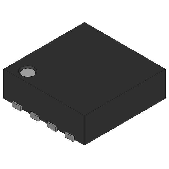
TPS2062A/TPS2066A
DRB PACKAGE
(TOP VIEW)
GND
IN
EN1
EN2
1
2
3
4
PAD
8
7
6
5
OC1
OUT1
OUT2
OC2
Enable inputs are active low for all TPS2062A
and active high for all TPS2066A
DESCRIPTION
The TPS206xA power-distribution switches are intended for applications where heavy capacitive loads and
short-circuits are likely to be encountered. The TPS206xA family is pin-for-pin compatible with the TPS206x
family with a tighter overcurrent tolerance. This family of devices incorporates two 70-mΩ N-channel MOSFET
power switches for power-distribution systems that require multiple power switches in a single package. Each
switch is controlled by a logic enable input. Gate drive is provided by an internal charge pump designed to
control the power-switch rise and fall times to minimize current surges during switching. The charge pump
requires no external components and allows operation from supplies as low as 2.7 V.
Each device limits the output current to a safe level by switching into a constant-current mode when the output
load exceeds the current-limit threshold or a short is present. Individual channels indicate the presence of an
overcurrent condition by asserting its corresponding OCx output (active low). Thermal protection circuitry
disables the device during overcurrent or short-circuit events to prevent permanent damage. The device recovers
from thermal shutdown automatically once the device has cooled sufficiently. The device provides undervoltage
lockout to disable the device until the input voltage rises above 2.0 V. The TPS206xA is designed to current limit
at 1.6 A typically per channel.
TPS201xA
TPS202x
TPS203x
0.2 A - 2 A
0.2 A - 2 A
0.2 A - 2 A
TPS2014
TPS2015
TPS2041B
TPS2051B
TPS2045A
TPS2049
TPS2055A
TPS2061
TPS2065
TPS2068
TPS2069
600 mA
1A
500 mA
500 mA
250 mA
100 mA
250 mA
1A
1A
1.5 A
1.5 A
1
2
Please be aware that an important notice concerning availability, standard warranty, and use in critical applications of Texas
Instruments semiconductor products and disclaimers thereto appears at the end of this data sheet.
PowerPAD is a trademark of Texas Instruments.
PRODUCTION DATA information is current as of publication date.
Products conform to specifications per the terms of the Texas
Instruments standard warranty. Production processing does not
necessarily include testing of all parameters.
Copyright © 2008, Texas Instruments Incorporated
�TPS2062A
TPS2066A
SLVS798F – JANUARY 2008 – REVISED NOVEMBER 2008 ........................................................................................................................................... www.ti.com
This device contains circuits to protect its inputs and outputs against damage due to high static voltages or electrostatic fields.
These circuits have been qualified to protect this device against electrostatic discharges (ESD) of up to 2 kV according to
MIL-STD-883C, Method 3015; however, it is advised that precautions be taken to avoid application of any voltage higher than
maximum-rated voltages to these high-impedance circuits. During storage or handling the device leads should be shorted together
or the device should be placed in conductive foam. In a circuit, unused inputs should always be connected to an appropriate logic
voltage level, preferably either VCC or ground. Specific guidelines for handling devices of this type are contained in the publication
Guidelines for Handling Electrostatic-Discharge-Sensitive (ESDS) Devices and Assemblies available from Texas Instruments.
AVAILABLE OPTION AND ORDERING INFORMATION
TA
ENABLE
(1)
TYPICAL
SHORT-CIRCUIT
LIMIT
1A
1.6 A
Active
low
–40°C to
85°C
PACKAGE (1)
RECOMMENDED
MAXIMUM
CONTINUOUS LOAD
CURRENT
Active
high
D-8
(SOIC)
DRB-8
(SON)
PART #
STATUS
PART #
STATUS
TPS2062AD
AVAILABLE
TPS2062ADRB
AVAILABLE
TPS2066AD
AVAILABLE
TPS2066ADRB
AVAILABLE
For the most current package and ordering information, see the Package Option Addendum at the end of this document, or see the TI
website at www.ti.com.
ABSOLUTE MAXIMUM RATINGS
over operating temperature range unless otherwise noted (1) (2)
VALUE
UNIT
VI
Input voltage range
IN
–0.3 to 6
V
VO
Output voltage range
OUTx
–0.3 to 6
V
Input voltage range
ENx, ENx
–0.3 to 6
V
Voltage range
OCx
–0.3 to 6
V
Continuous output current
OUTx
VI
IO
Internally limited
Continuous total power dissipation
See "Dissipation Rating Table"
TJ
Operating junction temperature range
–40 to 125
Tstg
Storage temperature range
–65 to 150
°C
2
kV
500
V
ESD
(1)
(2)
Human body model MIL-STD-883C
Electrostatic discharge
protection
Charge device model (CDM)
°C
Stresses beyond those listed under absolute maximum ratings may cause permanent damage to the device. These are stress ratings
only, and functional operation of the device at these or any other conditions beyond those indicated under recommended operating
conditions is not implied. Exposure to absolute-maximum-rated conditions for extended periods may affect device reliability.
All voltages are with respect to GND.
DISSIPATION RATING TABLE
PACKAGE
Low-K (1)
D-8
170 °C/W
High-K (2)
D-8
97.5 °C/W
Low-K
(3)
High-K (5)
(1)
(2)
(3)
(4)
(5)
2
THERMAL
RESISTANCE θJA
BOARD
DRB
(4)
DRB (4)
TA ≤ 25°C
POWER
RATING
DERATING
FACTOR
ABOVE TA =
25°C
TA = 70°C
POWER
RATING
TA = 85°C
POWER
RATING
586 mW
5.86 mW/°C
320 mW
234 mW
1025 mW
10.26 mW/°C
564 mW
410 mW
270 °C/W
370 mW
3.71 mW/°C
203 mW
148 mW
60 °C/W
1600 mW
16.67 mW/°C
916 mW
666 mW
The JEDEC low-K (1s) board used to dervie this data was a 3in x 3in, two-layer board with 2-ounce copper traces on top of the board.
The JEDEC high-K (2s2p) board used to dervive this data was a 3in x 3in, multilayer board with 1-ounce internal power and ground
planes and 2-ounce copper traces on top and bottom of the board.
Soldered PowerPAD on a standard 2-layer PCB without vias for thermal pad. See TI application note SLMA002 for further details.
See Recommended Operating Conditions Table for PowePad connection guidelines to meet qualifying conditions for CB Certificate
Soldered PowerPAD on a standard 4-layer PCB with vias for thermal pad. See TI application note SLMA002 for further details.
Submit Documentation Feedback
Copyright © 2008, Texas Instruments Incorporated
Product Folder Link(s): TPS2062A TPS2066A
�TPS2062A
TPS2066A
www.ti.com ........................................................................................................................................... SLVS798F – JANUARY 2008 – REVISED NOVEMBER 2008
RECOMMENDED OPERATING CONDITIONS (1)
Input voltage, IN
MIN
MAX
UNIT
2.7
5.5
V
Input voltage, ENx, ENx
0
5.5
V
IO
Continuous output current, OUTx
0
1
A
TJ
Operating virtual junction temperature
–40
125
°C
VI
(1)
The PowePad must be connected externally to GND pin to meet qualifying conditions for CB Certificate (DRB package only)
ELECTRICAL CHARACTERISTICS
over recommended operating junction temperature range, VI = 5.5 V, IO = 1 A, V/ENx = 0 V (TPS2062A) or VENx = 5.5 V
(unless otherwise noted)
TEST CONDITIONS (1)
PARAMETER
MIN
TYP
MAX
70
100
UNIT
POWER SWITCH
rDS(on)
Static drain-source on-state resistance 2.7 V ≤ VI ≤ 5.5 V, IO = 1 A
tr
Rise time, output
tf
Fall time, output
TJ = 25°C
–40°C ≤ TJ ≤ 125°C
135
VI = 5.5 V
VI = 2.7 V
VI = 5.5 V
0.6
0.4
CL = 1 µF,
RL = 5 Ω, TJ = 25°C
VI = 2.7 V
mΩ
1.5
1
0.05
0.5
0.05
0.5
ms
ENABLE INPUT EN OR EN
VIH
High-level input voltage
VIL
Low-level input voltage
II
Input current
ton
Turnon time
toff
Turnoff time
2
2.7 V ≤ VI ≤ 5.5 V
0.8
-0.5
0.5
3
CL = 100 µF, RL = 5 Ω
3
V
µA
ms
CURRENT LIMIT
IOS
Short-circuit output current per
channel
VI = 5 V, OUTx connected to GND,
device enabled into short-circuit
IOC
Overcurrent trip threshold
VIN = 5 V
IOS_G
Ganged short-circuit output current
VI = 5 V, OUT1 & OUT2 connected to
GND, device enabled into short-circuit
IOC_G
Ganged overcurrent trip threshold
VI = 5 V, OUT1 & OUT2 tied together
TJ = 25°C
1.2
1.6
2.0
–40°C ≤ TJ ≤ 125°C
1.1
1.6
2.1
IOS
2.1
2.45
TJ = 25°C
2.4
3.2
4.0
2.2
3.2
4.2
IOS_G
4.2
4.9
TJ = 25°C
0.5
1
–40°C ≤ TJ ≤ 125°C
0.5
5
TJ = 25°C
50
60
–40°C ≤ TJ ≤ 125°C
50
75
–40°C ≤ TJ ≤ 125°C
A
A
A
SUPPLY CURRENT
IIL
Supply current, device disabled
No load on OUT
IIH
Supply current, device enabled
No load on OUT
Ilkg
Leakage current, device disabled
OUT connected to ground
–40°C ≤ TJ ≤ 125°C
VO = 5.5 V, VI = 0 V
TJ = 25°C
Reverse leakage current
µA
µA
1
µA
0.2
µA
UNDERVOLTAGE LOCKOUT
Low-level input voltage, IN
VI rising
Hysteresis, IN
VI falling
2
2.5
75
V
mV
OVERCURRENT FLAG
VOL
Output low voltage, OC
I/OCx = 5 mA
Off-state current
V/OCx = 5.0 V or 3.3 V
OC deglitch
OCx assertion or de-assertion
4
8
0.4
V
1
µA
15
ms
THERMAL SHUTDOWN (2)
Thermal shutdown threshold
135
Recovery from thermal shutdown
125
Hysteresis
(1)
(2)
°C
°C
10
°C
Pulsed load testing used to maintain junction temperature close to ambient
The thermal shutdown only reacts under overcurrent conditions.
Submit Documentation Feedback
Copyright © 2008, Texas Instruments Incorporated
Product Folder Link(s): TPS2062A TPS2066A
3
�TPS2062A
TPS2066A
SLVS798F – JANUARY 2008 – REVISED NOVEMBER 2008 ........................................................................................................................................... www.ti.com
DEVICE INFORMATION
Terminal Functions
TERMINAL
NAME
I/O
DESCRIPTION
TPS2062A
TPS2066A
EN1
3
—
I
Enable input, logic low turns on power switch IN-OUT1
EN2
4
—
I
Enable input, logic low turns on power switch IN-OUT2
EN1
—
3
I
Enable input, logic high turns on power switch IN-OUT1
EN2
—
4
I
Enable input, logic high turns on power switch IN-OUT2
GND
1
1
IN
2
2
I
Input voltage
OC1
8
8
O
Channel 1 over-current indicator; the output is open-drain, active low type
OC2
5
5
O
Channel 2 over-current indicator; the output is open-drain, active low type
OUT1
7
7
O
Power-switch output, IN-OUT1
OUT2
6
6
O
Power-switch output, IN-OUT2
PAD
PAD
PowerPAD™
(1)
(1)
Ground
Connect PowerPAD to GND for proper operation (DRB package only)
See the Recommended Operating Conditions Table for PowePad connection guidelines to meet qualifying conditions for CB Certificate.
FUNCTIONAL BLOCK DIAGRAM
FAULT 1
Thermal
Sense
GND
Deglitch
EN1
Driver
Current
Limit
Charge
Pump
CS
OUT1
Current
Sense
UVLO
CS
IN
OUT2
Charge
Pump
EN2
Driver
Current
Limit
FAULT 2
Deglitch
Thermal
Sense
4
A.
Current sense
B.
Active low (ENx) for TPS2062A. Active high (ENx) for TPS2066A.
Submit Documentation Feedback
Copyright © 2008, Texas Instruments Incorporated
Product Folder Link(s): TPS2062A TPS2066A
�TPS2062A
TPS2066A
www.ti.com ........................................................................................................................................... SLVS798F – JANUARY 2008 – REVISED NOVEMBER 2008
PARAMETER MEASUREMENT INFORMATION
OUT
RL
CL
tr
tf
V OUT
90%
90%
10%
10%
TEST CIRCUIT
V EN
50%
50%
ton
50%
50%
V EN
toff
toff
ton
90%
90%
V OUT
V OUT
10%
10%
VOLTAGE WAVEFORMS
Figure 1. Test Circuit and Voltage Waveforms
RL = 5W,
CL = 1mF,
TA = 25°C
VI(EN)
5 V/div
VI(EN)
5 V/div
RL = 5W ,
CL = 1 mF
TA = 25°C
VO(OUT)
2 V/div
VO(OUT)
2 V/div
t − Time − 500 ms/div
t − Time − 500 ms/div
Figure 2. Turnon Delay and Rise Time With 1-µF Load
Figure 3. Turnoff Delay and Fall Time With 1-µF Load
Submit Documentation Feedback
Copyright © 2008, Texas Instruments Incorporated
Product Folder Link(s): TPS2062A TPS2066A
5
�TPS2062A
TPS2066A
SLVS798F – JANUARY 2008 – REVISED NOVEMBER 2008 ........................................................................................................................................... www.ti.com
PARAMETER MEASUREMENT INFORMATION (continued)
RL = 5W,
CL = 100 mF,
TA = 25°C
VI(EN)
5 V/div
VI(EN)
5 V/div
RL = 5W,
VO(OUT)
2 V/div
CL = 100 mF,
TA = 25°C
VO(OUT)
2 V/div
t − Time − 500 ms/div
t − Time − 500 ms/div
Figure 4. Turnon Delay and Rise Time With 100-µF Load
VI(EN)
5 V/div
Figure 5. Turnoff Delay and Fall Time With 100-µF Load
VIN = 5 V,
RL = 5W ,
TA = 25°C
VI(EN)
5 V/div
220 mF
470 mF
IO(OUT)
500 mA/div
IO(OUT)
500 mA/div
100 mF
t − Time − 500 ms/div
Figure 6. Short-Circuit Current,
Device Enabled Into Short
6
t − Time − 1 ms/div
Figure 7. Inrush Current With Different
Load Capacitance
Submit Documentation Feedback
Copyright © 2008, Texas Instruments Incorporated
Product Folder Link(s): TPS2062A TPS2066A
�TPS2062A
TPS2066A
www.ti.com ........................................................................................................................................... SLVS798F – JANUARY 2008 – REVISED NOVEMBER 2008
PARAMETER MEASUREMENT INFORMATION (continued)
VO(OC)
2 V/div
VO(OC)
2 V/div
IO(OUT)
1 A/div
IO(OUT)
1 A/div
t − Time − 2 ms/div
t − Time − 2 ms/div
Figure 8. 2-Ω Load Connected to Enabled Device
Figure 9. 1-Ω Load Connected to Enabled Device
POWER-SUPPLY CONSIDERATIONS
TPS2062A
2
Power Supply
2.7 V to 5.5 V
IN
OUT1
0.1 mF
8
3
5
4
7
Load
0.1 mF
22 mF
0.1 mF
22 mF
OC1
EN1
OUT2
6
OC2
Load
EN2
GND
1
Figure 10. Typical Application
DETAILED DESCRIPTION
OVERVIEW
The devices are current-limited, power distribution switches using N-channel MOSFETs for applications where
short-circuits or heavy capacitive loads will be encountered. These devices have a minimum fixed current-limit
threshold above 1.1 A allowing for continuous operation up to 1 A per channel. Overtemperature protection is an
addtional device shutdown feature. Each device incorporates an internal charge pump and gate drive circuitry
necessary to drive the N-channel MOSFETs. The charge pump supplies power to the driver circuit and provides
the necessary voltage to pull the gate of the MOSFET above the source. The charge pump operates from input
voltages as low as 2.7 V and requires little supply current. The driver controls the gate voltage of the power
switch. The driver incorporates circuitry that controls the rise and fall times of the output voltage to provide
"soft-start" and to limit large current and voltage surges.
Submit Documentation Feedback
Copyright © 2008, Texas Instruments Incorporated
Product Folder Link(s): TPS2062A TPS2066A
7
�TPS2062A
TPS2066A
SLVS798F – JANUARY 2008 – REVISED NOVEMBER 2008 ........................................................................................................................................... www.ti.com
OVERCURRENT
When an overcurrent condition is detected, the device maintains a constant output current and reduces the
output voltage accordingly. Three possible overload conditions can occur.
In the first condition, the output has been shorted before the device is enabled or before voltage is applied to IN.
The device senses the short and immediately switches into a constant-current output. In the second condition, a
short or an overload occurs while the device is enabled. At the instant the overload occurs, high currents may
flow for several microseconds before the current-limit circuit can react. The device operates in constant-current
mode after the current-limit circuit has responded. In the third condition, the load is increased gradually beyond
the recommended operating current. The current is permitted to rise until the current-limit threshold is reached.
The devices are capable of delivering current up to the current-limit threshold without damage. Once the
threshold is reached, the device switches into constant-current mode.
Complete shutdown occurs only if the fault is present long enough to activate thermal limiting. The device will
remain off until the junction temperature cools approximately 10°C and will then re-start. The device will continue
to cycle on/off until the overcurrent condition is removed.
OCx RESPONSE
Each OCx open-drain output is asserted (active low) during an overcurrent or overtemperature condition on that
channel. The output remains asserted until the fault condition is removed. The TPS206xA eliminates false OCx
reporting by using internal delay circuitry after entering or leaving an overcurrent condition. This "deglitch" time is
approximately 8-ms. This ensures that OCx is not accidentally asserted due to normal operation such as starting
into a heavy capacitive load. Overtemperature conditions are not deglitched and assert and de-assert the OCx
signal immediately.
UNDERVOLTAGE LOCKOUT (UVLO)
The undervoltage lockout (UVLO) circuit disables the power switch until the input voltage reaches the UVLO
turn-on threshold. Built-in hysteresis prevents unwanted on/off cycling due to input voltage drop from large
current surges.
Enable (ENx or ENx)
The logic enable controls the power switch, bias for the charge pump, driver, and other circuits to reduce the
supply current. The supply current is reduced to less than 5 µA when a logic high is present on ENx, or when a
logic low is present on ENx. A logic low input on ENx or a logic high input on ENx enables the driver, control
circuits, and power switch for that channel.
THERMAL SENSE
The TPS206xA monitors the operating temperature of both power distribution switches with individual thermal
sensors. The junction temperature of each channel rises during an overcurrent or short-circuit condition. When
the die temperature of a particular channel rises above a minimum of 135°C in an overcurrent condition, the
internal thermal sense circuitry disables the individual channel in overtemperature to prevent damage. Hysteresis
is built into the thermal sensor and re-enables the power switch individually after it has cooled approximately
10°C. The power switch cycles on and off until the fault is removed. This topology allows one channel to continue
normal operation even if the other channel is in an overtemperature condition. The open-drain overcurrent flag
(OCx) is asserted (active low) corresponding to the channel that is in an overtemperature or overcurrent
condition.
8
Submit Documentation Feedback
Copyright © 2008, Texas Instruments Incorporated
Product Folder Link(s): TPS2062A TPS2066A
�TPS2062A
TPS2066A
www.ti.com ........................................................................................................................................... SLVS798F – JANUARY 2008 – REVISED NOVEMBER 2008
TYPICAL CHARACTERISTICS
TURNON TIME
vs
INPUT VOLTAGE
TURNOFF TIME
vs
INPUT VOLTAGE
1.0
2
CL = 100 mF,
RL = 5W ,
TA = 25 °C
0.9
1.9
0.7
Turnoff Time − mS
Turnon Time − ms
0.8
CL = 100 mF,
RL = 5W ,
TA = 25 °C
0.6
0.5
0.4
0.3
0.2
1.8
1.7
1.6
0.1
0
2
3
4
5
VI − Input Voltage − V
1.5
6
2
4
5
VI − Input Voltage − V
Figure 11.
Figure 12.
RISE TIME
vs
INPUT VOLTAGE
FALL TIME
vs
INPUT VOLTAGE
6
0.25
0.6
CL = 1mF,
RL = 5W ,
TA = 25°C
CL = 1 mF,
RL = 5W ,
TA = 25 °C
0.5
0.2
0.4
Fall Time − ms
Rise Time − ms
3
0.3
0.15
0.1
0.2
0.05
0.1
0
0
2
3
4
5
VI − Input Voltage − V
6
2
Figure 13.
3
4
5
VI − Input Voltage − V
6
Figure 14.
Submit Documentation Feedback
Copyright © 2008, Texas Instruments Incorporated
Product Folder Link(s): TPS2062A TPS2066A
9
�TPS2062A
TPS2066A
SLVS798F – JANUARY 2008 – REVISED NOVEMBER 2008 ........................................................................................................................................... www.ti.com
TYPICAL CHARACTERISTICS (continued)
TPS2062A, TPS2066A
SUPPLY CURRENT, OUTPUT ENABLED
vs
JUNCTION TEMPERATURE
TPS2062A, TPS2066A
SUPPLY CURRENT, OUTPUT DISABLED
vs
JUNCTION TEMPERATURE
I I (IN) − Supply Current, Output Disabled − m A
I I (IN) − Supply Current, Output Enabled − m A
70
VI = 5.5 V
60
50
VI = 5 V
VI = 3.3 V
40
30
VI = 2.7 V
20
10
0
−50
0
50
100
0.5
VI = 5.5 V
0.45
VI = 5 V
0.4
0.35
0.3
0.25
0.2
0.15
0.1
0.05
0
−50
150
VI = 3.3 V
VI = 2.7 V
0
Figure 15.
On-State Resistance − m Ω
100
r DS(on) − Static Drain-Source
150
SHORT-CIRCUIT OUTPUT CURRENT
vs
JUNCTION TEMPERATURE
1.56
I OS − Short-Circuit Output Current −A
Out1 = 5 V
Out1 = 3.3 V
80
100
Figure 16.
STATIC DRAIN-SOURCE ON-STATE RESISTANCE
vs
JUNCTION TEMPERATURE
120
IO = 0.5 A
50
TJ − Junction Temperature − °C
TJ − Junction Temperature − °C
Out1 = 2.7 V
60
40
20
VI = 2.7 V
1.54
1.52
VI = 3.3 V
1.5
1.48
1.46
1.44
VI = 5 V
1.42
VI = 5.5 V
1.4
1.38
1.36
0
1.34
−50
0
50
100
150
−50
TJ − Junction Temperature −°C
Figure 17.
10
0
50
100
150
TJ − Junction Temperature −°C
Figure 18.
Submit Documentation Feedback
Copyright © 2008, Texas Instruments Incorporated
Product Folder Link(s): TPS2062A TPS2066A
�TPS2062A
TPS2066A
www.ti.com ........................................................................................................................................... SLVS798F – JANUARY 2008 – REVISED NOVEMBER 2008
TYPICAL CHARACTERISTICS (continued)
THRESHOLD TRIP CURRENT
vs
INPUT VOLTAGE
UNDERVOLTAGE LOCKOUT
vs
JUNCTION TEMPERATURE
2.3
2.5
UVLO Rising
UVOL − Undervoltage Lockout − V
TA = 25°C
Load Ramp = 1A/10 ms
Threshold Trip Current − A
2.3
2.1
1.9
1.7
1.5
2.5
3
3.5
4
4.5
5
5.5
6
2.26
2.22
UVLO Falling
2.18
2.14
2.1
−50
0
50
100
150
TJ − Junction Temperature − °C
VI − Input Voltage − V
Figure 19.
Figure 20.
CURRENT-LIMIT RESPONSE
vs
PEAK CURRENT
200
Current-Limit Response − m s
VI = 5 V,
TA = 25°C
150
100
50
0
0
2.5
5
7.5
Peak Current − A
Figure 21.
10
12.5
Submit Documentation Feedback
Copyright © 2008, Texas Instruments Incorporated
Product Folder Link(s): TPS2062A TPS2066A
11
�TPS2062A
TPS2066A
SLVS798F – JANUARY 2008 – REVISED NOVEMBER 2008 ........................................................................................................................................... www.ti.com
APPLICATION INFORMATION
INPUT AND OUTPUT CAPACITANCE
Input and output capacitance improve the performance of the device; the actual capacitance should be optimized
for the particular application. For all applications, a 0.01 µF to 0.1 µF ceramic bypass capacitor between IN and
GND is recommended and should be placed as close to the device as possible for local noise de-coupling. This
precaution reduces ringing on the input due to power-supply transients . Additional input capacitance may be
needed on the input to reduce voltage overshoot from exceeding the absolute maximum voltage of the device
during heavy transients.
Placing a high-value electrolytic capacitor on the output pin is recommended when the output load is heavy.
Additionally, bypassing the output with a 0.01 µF to 0.1 µF ceramic capacitor improves the immunity of the
device to short-circuit transients.
POWER DISSIPATION AND JUNCTION TEMPERATURE
The low on-resistance of the N-channel MOSFETs allows the small surface-mount packages to pass large
currents. It is good design practice to check power dissipation to ensure that the junction temperature of the
device is within the recommended operating conditions. The below analysis gives an approximation for
calculating junction temperature based on the power dissipation in the package. However, it is important to note
that thermal analysis is strongly dependent on additional system level factors. Such factors include air flow,
board layout, copper thickness and surface area, and proximity to other devices dissipating power. Good thermal
design practice must include all system level factors in addition to individual component analysis.
The following procedure shows how to approximate the junction temperature rise due to power dissipation in a
single channel. The TPS2062A/66A devices contain two channels, so the total device power must sum the power
in each power switch.
Begin by determining the rDS(on) of the N-channel MOSFET relative to the input voltage and operating
temperature. Use the highest operating ambient temperature of interest and read rDS(on) from the typical
characteristics graph as an initial estimate. Power dissipation is calculated by:
PD = rDS(on)× IOUT2
PT = 2 x PD
Where:
PD = Power dissipation/channel (W)
PT = Total power dissipation for both channels (W)
rDS(on) = Power switch on-resistance (Ω)
IOUT = Maximum current-limit threshold (A)
Finally, calculate the junction temperature:
TJ = PT x RΘJA + TA
Where:
TA= Ambient temperature °C
RΘJA = Thermal resistance (°C/W)
PT = Total power dissipation (W)
Compare the calculated junction temperature with the initial estimate. If they are not within a few degrees, repeat
the calculation using the "refined" rDS(on) from the previous calculation as the new estimate. Two or three
iterations are generally sufficient to achieve the desired result. The final junction temperature is highly dependent
on thermal resistance RθJA, and thermal resistance is highly dependent on the individual package and board
layout. The "Dissipation Rating Table" at the begginng of this document provides example thermal resistances for
specific packages and board layouts.
12
Submit Documentation Feedback
Copyright © 2008, Texas Instruments Incorporated
Product Folder Link(s): TPS2062A TPS2066A
�TPS2062A
TPS2066A
www.ti.com ........................................................................................................................................... SLVS798F – JANUARY 2008 – REVISED NOVEMBER 2008
UNIVERSAL SERIAL BUS (USB) APPLICATIONS
One application for this device is for current-limiting in universal serial bus (USB) applications. The original USB
interface was a 12-Mb/s or 1.5-Mb/s, multiplexed serial bus designed for low-to-medium bandwidth PC
peripherals (e.g., keyboards, printers, scanners, and mice). As the demand for more bandwidth increased, the
USB 2.0 standard was introduced increasing the maximum data rate to 480-Mb/s. The four-wire USB interface is
conceived for dynamic attach-detach (hot plug-unplug) of peripherals. Two lines are provided for differential data,
and two lines are provided for 5-V power distribution.
USB data is a 3.3-V level signal, but power is distributed at 5 V to allow for voltage drops in cases where power
is distributed through more than one hub across long cables. Each function must provide its own regulated 3.3 V
from the 5-V input or its own internal power supply. The USB specification classifies two different classes of
devices depending on its maximum current draw. A device classified as low-power can draw up to 100 mA as
defined by the standard. A device classified as high-power can draw up to 500 mA. It is important that the
minimum current limit threshold of the current-limiting power switch exceed the maximum current limit draw of the
intended application. The latest USB standard should always be referenced when considering the current-limit
threshold.
The USB specification defines two types of devices as hubs and functions. A USB hub is a device that contains
multiple ports for different USB devices to connect and can be self-powered (SPH) or bus-powered (BPH). A
function is a USB device that is able to transmit or receive data or control information over the bus. A USB
function can be embedded in a USB hub. A USB function can be one of three types included in the list below.
• Low-power, bus-powered function
• High-power, bus-powered function
• Self-powered function
SPHs and BPHs distribute data and power to downstream functions. The TPS206x6A has higher current
capability than required for a single USB port allowing it to power multiple downstream ports.
SELF-POWERED AND BUS-POWERED HUBS
A SPH has a local power supply that powers embedded functions and downstream ports. This power supply
must provide between 4.75 V to 5.25 V to downstream facing devices under full-load and no-load conditions.
SPHs are required to have current-limit protection and must report overcurrent conditions to the USB controller.
Typical SPHs are desktop PCs, monitors, printers, and stand-alone hubs.
A BPH obtains all power from an upstream port and often contains an embedded function. It must power up with
less than 100 mA. The BPH usually has one embedded function, and power is always available to the controller
of the hub. If the embedded function and hub require more than 100 mA on power up, the power to the
embedded function may need to be kept off until enumeration is completed. This is accomplished by removing
power or by shutting off the clock to the embedded function. Power switching the embedded function is not
necessary if the aggregate power draw for the function and controller is less than 100 mA. The total current
drawn by the bus-powered device is the sum of the current to the controller, the embedded function, and the
downstream ports, and it is limited to 500 mA from an upstream port.
LOW-POWER BUS-POWERED AND HIGH-POWER BUS-POWERED FUNCTIONS
Both low-power and high-power bus-powered functions obtain all power from upstream ports. Low-power
functions always draw less than 100 mA; high-power functions must draw less than 100 mA at power up and can
draw up to 500 mA after enumeration. If the load of the function is more than the parallel combination of 44 Ω
and 10 µF at power up, the device must implement inrush current limiting.
Submit Documentation Feedback
Copyright © 2008, Texas Instruments Incorporated
Product Folder Link(s): TPS2062A TPS2066A
13
�TPS2062A
TPS2066A
SLVS798F – JANUARY 2008 – REVISED NOVEMBER 2008 ........................................................................................................................................... www.ti.com
USB POWER-DISTRIBUTION REQUIREMENTS
USB can be implemented in several ways regardless of the type of USB device being developed. Several
power-distribution features must be implemented.
• SPHs must:
– Current-limit downstream ports
– Report overcurrent conditions
• BPHs must:
– Enable/disable power to downstream ports
– Power up at