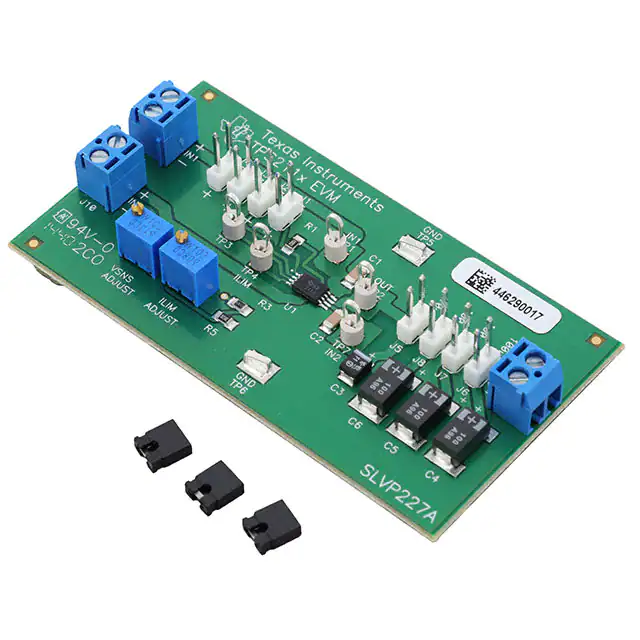
TPS211xEVM
Power Multiplexer Evaluation Module
User’s Guide
November 2002
PMP EVMs
SLLU054
�IMPORTANT NOTICE
Texas Instruments Incorporated and its subsidiaries (TI) reserve the right to make corrections, modifications,
enhancements, improvements, and other changes to its products and services at any time and to discontinue
any product or service without notice. Customers should obtain the latest relevant information before placing
orders and should verify that such information is current and complete. All products are sold subject to TI’s terms
and conditions of sale supplied at the time of order acknowledgment.
TI warrants performance of its hardware products to the specifications applicable at the time of sale in
accordance with TI’s standard warranty. Testing and other quality control techniques are used to the extent TI
deems necessary to support this warranty. Except where mandated by government requirements, testing of all
parameters of each product is not necessarily performed.
TI assumes no liability for applications assistance or customer product design. Customers are responsible for
their products and applications using TI components. To minimize the risks associated with customer products
and applications, customers should provide adequate design and operating safeguards.
TI does not warrant or represent that any license, either express or implied, is granted under any TI patent right,
copyright, mask work right, or other TI intellectual property right relating to any combination, machine, or process
in which TI products or services are used. Information published by TI regarding third-party products or services
does not constitute a license from TI to use such products or services or a warranty or endorsement thereof.
Use of such information may require a license from a third party under the patents or other intellectual property
of the third party, or a license from TI under the patents or other intellectual property of TI.
Reproduction of information in TI data books or data sheets is permissible only if reproduction is without
alteration and is accompanied by all associated warranties, conditions, limitations, and notices. Reproduction
of this information with alteration is an unfair and deceptive business practice. TI is not responsible or liable for
such altered documentation.
Resale of TI products or services with statements different from or beyond the parameters stated by TI for that
product or service voids all express and any implied warranties for the associated TI product or service and
is an unfair and deceptive business practice. TI is not responsible or liable for any such statements.
Mailing Address:
Texas Instruments
Post Office Box 655303
Dallas, Texas 75265
Copyright 2002, Texas Instruments Incorporated
�EVM IMPORTANT NOTICE
Texas Instruments (TI) provides the enclosed product(s) under the following conditions:
This evaluation kit being sold by TI is intended for use for ENGINEERING DEVELOPMENT OR EVALUATION
PURPOSES ONLY and is not considered by TI to be fit for commercial use. As such, the goods being provided
may not be complete in terms of required design-, marketing-, and/or manufacturing-related protective
considerations, including product safety measures typically found in the end product incorporating the goods.
As a prototype, this product does not fall within the scope of the European Union directive on electromagnetic
compatibility and therefore may not meet the technical requirements of the directive.
Should this evaluation kit not meet the specifications indicated in the EVM User’s Guide, the kit may be returned
within 30 days from the date of delivery for a full refund. THE FOREGOING WARRANTY IS THE EXCLUSIVE
WARRANTY MADE BY SELLER TO BUYER AND IS IN LIEU OF ALL OTHER WARRANTIES, EXPRESSED,
IMPLIED, OR STATUTORY, INCLUDING ANY WARRANTY OF MERCHANTABILITY OR FITNESS FOR ANY
PARTICULAR PURPOSE.
The user assumes all responsibility and liability for proper and safe handling of the goods. Further, the user
indemnifies TI from all claims arising from the handling or use of the goods. Please be aware that the products
received may not be regulatory compliant or agency certified (FCC, UL, CE, etc.). Due to the open construction
of the product, it is the user’s responsibility to take any and all appropriate precautions with regard to electrostatic
discharge.
EXCEPT TO THE EXTENT OF THE INDEMNITY SET FORTH ABOVE, NEITHER PARTY SHALL BE LIABLE
TO THE OTHER FOR ANY INDIRECT, SPECIAL, INCIDENTAL, OR CONSEQUENTIAL DAMAGES.
TI currently deals with a variety of customers for products, and therefore our arrangement with the user is not
exclusive.
TI assumes no liability for applications assistance, customer product design, software performance, or
infringement of patents or services described herein.
Please read the EVM User’s Guide and, specifically, the EVM Warnings and Restrictions notice in the EVM
User’s Guide prior to handling the product. This notice contains important safety information about temperatures
and voltages. For further safety concerns, please contact the TI application engineer.
Persons handling the product must have electronics training and observe good laboratory practice standards.
No license is granted under any patent right or other intellectual property right of TI covering or relating to any
machine, process, or combination in which such TI products or services might be or are used.
Mailing Address:
Texas Instruments
Post Office Box 655303
Dallas, Texas 75265
Copyright 2002, Texas Instruments Incorporated
�EVM WARNINGS AND RESTRICTIONS
It is important to operate this EVM within the input voltage range between 2.8 V and 5.5 V and
the output voltage range of 2.8 V and 5.5 V.
Exceeding the specified input range may cause unexpected operation and/or irreversible
damage to the EVM. If there are questions concerning the input range, please contact a TI
field representative prior to connecting the input power.
Applying loads outside of the specified output range may result in unintended operation and/or
possible permanent damage to the EVM. Please consult the EVM User’s Guide prior to
connecting any load to the EVM output. If there is uncertainty as to the load specification,
please contact a TI field representative.
During normal operation, some circuit components may have case temperatures greater than
60°C. The EVM is designed to operate properly with certain components above 60°C as long
as the input and output ranges are maintained. These components include but are not limited
to linear regulators, switching transistors, pass transistors, and current sense resistors. These
types of devices can be identified using the EVM schematic located in the EVM User’s Guide.
When placing measurement probes near these devices during operation, please be aware
that these devices may be very warm to the touch.
Mailing Address:
Texas Instruments
Post Office Box 655303
Dallas, Texas 75265
Copyright 2002, Texas Instruments Incorporated
�Trademarks
Preface
Read This First
About This Manual
This user’s guide describes the TPS211x evaluation module (EVM). This
guide contains the EVM schematic, bill of materials, assembly drawing, and
top and bottom board layouts.
How to Use This Manual
This document contains the following chapters:
- Chapter 1- Introduction
- Chapter 2- EVM Setup
- Chapter 3- Schematic and Bill of Materials
- Chapter 4- Board Layout
The information in a caution or a warning is provided for your protection.
Please read each caution and warning carefully.
Related Documentation From Texas Instruments
TPS2110/1 Autoswitching Power Mux- data sheet (SLVS443)
TPS2112/3 Autoswitching Power Mux- data sheet (SLVS446)
TPS2114/5 Autoswitching Power Mux- data sheet (SLVS447)
Trademarks
Trademarks are the property of their respective owners.
v
�Trademarks
Electrostatic Sensitive Devices
This EVM contains components that can potentially be damaged by
electrostatic discharge. Always transport and store the EVM in its
supplied ESD bag when not in use. Handle using an antistatic
wristband. Operate on an antistatic work surface. For more
information on proper handling, refer to SSYA008.
vi
�Contents
Contents
1
Introduction . . . . . . . . . . . . . . . . . . . . . . . . . . . . . . . . . . . . . . . . . . . . . . . . . . . . . . . . . . . . . . . . . . . . . 1-1
2
EVM Setup . . . . . . . . . . . . . . . . . . . . . . . . . . . . . . . . . . . . . . . . . . . . . . . . . . . . . . . . . . . . . . . . . . . . . .
2.1
Setting Up the EVM . . . . . . . . . . . . . . . . . . . . . . . . . . . . . . . . . . . . . . . . . . . . . . . . . . . . . . . . .
2.2
Current-Limit Adjustment . . . . . . . . . . . . . . . . . . . . . . . . . . . . . . . . . . . . . . . . . . . . . . . . . . . .
2.3
Manual Switching Mode (TPS2110/1/4/5 Only) . . . . . . . . . . . . . . . . . . . . . . . . . . . . . . . . .
2.3.1 Configuring the TPS2110/1 for Manual Switching . . . . . . . . . . . . . . . . . . . . . . . .
2.3.2 Configuring the TPS2114/5 for Manual Switching . . . . . . . . . . . . . . . . . . . . . . . .
2.4
Automatic Switching Modes . . . . . . . . . . . . . . . . . . . . . . . . . . . . . . . . . . . . . . . . . . . . . . . . . .
2.4.1 Mode 1 Automatic Switching . . . . . . . . . . . . . . . . . . . . . . . . . . . . . . . . . . . . . . . . . .
2.4.2 Mode 2 Automatic Switching (TPS2110/1/2/3 Only) . . . . . . . . . . . . . . . . . . . . . .
2.5
Output Voltage Holdup . . . . . . . . . . . . . . . . . . . . . . . . . . . . . . . . . . . . . . . . . . . . . . . . . . . . . .
2.6
Switch Status (TPS2112/3/4/5 Only) . . . . . . . . . . . . . . . . . . . . . . . . . . . . . . . . . . . . . . . . . . .
2-1
2-2
2-2
2-3
2-3
2-3
2-3
2-3
2-4
2-4
2-4
3
Schematic and Bill of Materials . . . . . . . . . . . . . . . . . . . . . . . . . . . . . . . . . . . . . . . . . . . . . . . . . . .
3.1
EVM Configurations . . . . . . . . . . . . . . . . . . . . . . . . . . . . . . . . . . . . . . . . . . . . . . . . . . . . . . . . .
3.2
Schematic . . . . . . . . . . . . . . . . . . . . . . . . . . . . . . . . . . . . . . . . . . . . . . . . . . . . . . . . . . . . . . . . .
3.3
Bill of Materials . . . . . . . . . . . . . . . . . . . . . . . . . . . . . . . . . . . . . . . . . . . . . . . . . . . . . . . . . . . . .
3-1
3-2
3-2
3-3
4
Board Layout . . . . . . . . . . . . . . . . . . . . . . . . . . . . . . . . . . . . . . . . . . . . . . . . . . . . . . . . . . . . . . . . . . . 4-1
4.1
Layout Considerations . . . . . . . . . . . . . . . . . . . . . . . . . . . . . . . . . . . . . . . . . . . . . . . . . . . . . . 4-2
vii
�Contents
Figures
2-1
3-1
4-1
4-2
4-3
Basic EVM Setup . . . . . . . . . . . . . . . . . . . . . . . . . . . . . . . . . . . . . . . . . . . . . . . . . . . . . . . . . . . . .
TPS211xEVM Schematic . . . . . . . . . . . . . . . . . . . . . . . . . . . . . . . . . . . . . . . . . . . . . . . . . . . . . .
Component Placement . . . . . . . . . . . . . . . . . . . . . . . . . . . . . . . . . . . . . . . . . . . . . . . . . . . . . . . .
Top-Side Layout . . . . . . . . . . . . . . . . . . . . . . . . . . . . . . . . . . . . . . . . . . . . . . . . . . . . . . . . . . . . . .
Bottom-Side Layout . . . . . . . . . . . . . . . . . . . . . . . . . . . . . . . . . . . . . . . . . . . . . . . . . . . . . . . . . . .
2-2
3-2
4-2
4-2
4-2
Tables
2-1
2-2
3-1
3-2
viii
EVM Shorting Jumper Placement for Mode 1 Automatic Switching . . . . . . . . . . . . . . . . . .
EVM Shorting Jumper Placement for Mode 2 Automatic Switching . . . . . . . . . . . . . . . . . .
Available EVM Configurations . . . . . . . . . . . . . . . . . . . . . . . . . . . . . . . . . . . . . . . . . . . . . . . . . .
SLVP227 Bill of Materials . . . . . . . . . . . . . . . . . . . . . . . . . . . . . . . . . . . . . . . . . . . . . . . . . . . . . .
2-3
2-4
3-2
3-3
�Chapter 1
Introduction
The TPS211x EVM is an evaluation module for the Texas Instruments
TPS211x family of two-input, one-output power multiplexers. These
multiplexers enable seamless transition between two power supplies, each
operating at 2.8 V–5.5 V and delivering up to 1 A. EVM configurations are
available for the TPS2110 through TPS2115. Refer to Table 3-1, the
schematic, and the bill of materials in this user’s guide to distinguish between
these configurations.
The EVM has test points for convenient access to all critical node voltages,
potentiometers for adjusting the current limit and the auto-switching voltage
sense thresholds, headers for selecting the manual/auto-switching operating
modes, and headers for selecting the output hold-up capacitance.
Introduction
1-1
�1-2
�Chapter 2
EVM Setup
This chapter describes the proper setup of the TPS211xEVM for use in device
evaluations.
Topic
Page
2.1
Setting Up the EVM . . . . . . . . . . . . . . . . . . . . . . . . . . . . . . . . . . . . . . . . . . . 2-2
2.2
Current-Limit Adjustment . . . . . . . . . . . . . . . . . . . . . . . . . . . . . . . . . . . . . . 2-2
2.3
Manual Switching Mode (TPS2110/1/4/5 Only) . . . . . . . . . . . . . . . . . . . 2-2
2.4
Automatic Switching Modes . . . . . . . . . . . . . . . . . . . . . . . . . . . . . . . . . . . 2-3
2.5
Output Voltage Holdup . . . . . . . . . . . . . . . . . . . . . . . . . . . . . . . . . . . . . . . . 2-4
2.6
Switch Status (TPS2112/3/4/5 Only) . . . . . . . . . . . . . . . . . . . . . . . . . . . . . 2-4
EVM Setup
2-1
�Setting Up the EVM
2.1 Setting Up the EVM
The user is encouraged to read the applicable TPS211x data sheet before
using the EVM.
The following test equipment is recommended:
- Storage oscilloscope
- Current probe
- Two adjustable power supplies, 0V – 6 V @ 2-A
- Volt-Ohm meter
- A passive or active load
Figure 2-1 shows the EVM test set up.
Figure 2-1. Basic EVM Setup
V1
RL
V2
2.2 Current-Limit Adjustment
Potentiometer R4 controls the resistance RILIM that sets the TPS211x current
limit threshold. Adjusting R4 clockwise increases the current limit threshold by
decreasing RILIM. The current limit threshold is 250/RILIM for the TPS2110,
TPS2112, and TPS2114 and 500/RILIM for the TPS2111, TPS2113, and
TPS2115.
To measure the resistance RILIM, connect an ohmmeter between test points
TP4 and GND. The measurement should be made with the IN1 and IN2
supplies off. To ensure accurate in-circuit resistance measurements, the
ohmmeter must apply no more than 0.5 V across the resistor.
2-2
�Manual Switching Mode (TPS2110/1/4/5 Only)
2.3 Manual Switching Mode (TPS2110/1/4/5 Only)
Potentiometer R2 and header J4 have no effect upon the operation of the
manual switching mode.
Some products like digital cameras and palm computers that receive power
from an internal battery or from a docking station can take advantage of the
manual-switching feature. The TPS2110/1/4/5 digital control input, D1, can
directly sense the presence of the docking station and connect the load to the
appropriate power source.
2.3.1
Configuring the TPS2110/1 for Manual Switching
To place the device into manual switching mode, short header J1. The logic
level on the D1 pin now determines which input is selected. On the EVM,
header J2 controls the D1 pin. If J2 is left open, then D1 is internally pulled high
and IN1 is selected. If J2 is shorted, then D1 is pulled low and IN2 is selected.
2.3.2
Configuring the TPS2114/5 for Manual Switching
To place the device into manual switching mode, short header J2. The logic
level on the D1 pin determines which input is selected. On the EVM, header
J3 controls the D1 pin. If J3 is left open, then D1 is internally pulled high and
IN1 is selected. If J3 is shorted, then D1 is pulled low and IN2 is selected.
2.4 Automatic Switching Modes
All EVMs support Mode 1 automatic switching. Mode 2 automatic switching is
supported by the TPS2110–TPS2113 EVMs only.
2.4.1
Mode 1 Automatic Switching
OUT connects to the higher of IN1 and IN1 in Mode 1 automatic switching.
Refer to Table 2-1 to configure the EVM for Mode 1 automatic switching.
Table 2-1. EVM Shorting Jumper Placement for Mode 1 Automatic Switching
Header
EVM
Device
SLVP227-001
TPS2110
X
SLVP227-002
TPS2111
X
SLVP227-003
TPS2112
X
SLVP227-004
TPS2113
X
SLVP227-005
TPS2114
X
SLVP227-006
TPS2115
X
J1
J2
J3
J4
A manufacturer can provide a secondary battery pack option to extend the
product run time with Mode 1 automatic switching. The TPS211x cycles
between the primary and secondary batteries until both batteries are drained.
EVM Setup
2-3
�Output Voltage Holdup
2.4.2
Mode 2 Automatic Switching (TPS2110/1/2/3 Only)
In Mode 2 automatic switching, OUT connects to IN1 if the voltage at IN1 is
sufficiently high, otherwise OUT connects to the higher of IN1 and IN2. The
threshold at which IN1 is selected corresponds to approximately 0.8 V at test
point TP3. The corresponding value of the IN1 voltage depends upon the
setting of potentiometer R2. Adjusting R2 clockwise increases the IN1
selection threshold voltage.
Refer to Table 2-2 to configure the EVM for Mode 2 automatic switching.
Table 2-2. EVM Shorting Jumper Placement for Mode 2 Automatic Switching
Header
EVM
Device
SLVP227-001
TPS2110
X
X
SLVP227-002
TPS2111
X
X
SLVP227-003
TPS2112
X
X
SLVP227-004
TPS2113
X
X
J1
J2
J3
J4
A manufacturer can provide a secondary battery pack option to extend the
product run time with Mode 2 automatic switching. The TPS2110–TPS2113
drains the primary battery at IN1 and automatically switches to the secondary
battery at IN2.
2.5 Output Voltage Holdup
Headers J5–J8 select the output holdup capacitance.
The output voltage drops out for 60 µs (max) whenever the TPS211x switches
between the IN1 and IN2 supplies. Some capacitance at the TPS211x output
is necessary to prevent the output voltage from dropping too much during the
supply switchover. Excessive voltage drop can cause a system to reset or lose
data.
2.6 Switch Status (TPS2112/3/4/5 Only)
The switch status output can be monitored at the positive terminal of header
J1. A switch status output equal to logic 1 corresponds to an IN2 switch that
is on.
2-4
�Chapter 3
Schematic and Bill of Materials
The TPS211xEVM schematic and bill of materials are provided in this chapter.
Topic
Page
3.1
EVM Configurations . . . . . . . . . . . . . . . . . . . . . . . . . . . . . . . . . . . . . . . . . . . 3-2
3.2
Schematic . . . . . . . . . . . . . . . . . . . . . . . . . . . . . . . . . . . . . . . . . . . . . . . . . . . . 3-2
3.3
Bill of Materials . . . . . . . . . . . . . . . . . . . . . . . . . . . . . . . . . . . . . . . . . . . . . . . 3-3
Schematic and Bill of Materials
3-1
�EVM Configurations
3.1 EVM Configurations
Table 3-1. Available EVM Configurations
Switching Modes
EVM
Designator
Device
Current-Limit Adjustment
Range
Switch Status
Output
Automatic
Manual
SLVP227-001
TPS2110
0.31 A–0.75 A
No
Yes
Yes
SLVP227-002
TPS2111
0.63 A–1.25 A
No
Yes
Yes
SLVP227-003
TPS2112
0.31 A–0.75 A
Yes
Yes
No
SLVP227-004
TPS2113
0.63 A–1.25 A
Yes
Yes
No
SLVP227-005
TPS2114
0.31 A–0.75 A
Yes
Yes
Yes
SLVP227-006
TPS2115
0.63 A–1.25 A
Yes
Yes
Yes
3.2 Schematic
Figure 3-1. TPS211xEVM Schematic
3-2
U1
R1
R2
R3
R5
Current-Limit
TPS2110
—
10KΩ
887
332
0.31 A–0.75 A
TPS2111
—
10KΩ
681
392
0.63 A–1.25 A
TPS2112
10KΩ
10KΩ
887
332
0.31 A–0.75 A
TPS2113
10KΩ
10KΩ
681
392
0.63 A–1.25 A
TPS2114
10KΩ
—
887
332
0.31 A–0.75 A
TPS2115
10KΩ
—
681
392
0.63 A–1.25 A
�Bill of Materials
3.3 Bill of Materials
Table 3-2. SLVP227 Bill of Materials
Quantity
-001
-002
-003
-004
-005
-006
Description
MFG
MFG PART #
Size
1
0
0
0
0
0
IC, Power mux
Texas
Instruments
TPS2110PW
PW-8
0
1
0
0
0
0
IC, Power mux
Texas
Instruments
TPS2111PW
PW-8
0
0
1
0
0
0
IC, Power mux
Texas
Instruments
TPS2112PW
PW-8
0
0
0
1
0
0
IC, Power mux
Texas
Instruments
TPS2113PW
PW-8
0
0
0
0
1
0
IC, Power mux
Texas
Instruments
TPS2114PW
PW-8
0
0
0
0
0
1
IC, Power mux
Texas
Instruments
TPS2115PW
PW-8
1
0
1
0
1
0
Resistor, 887 Ω,
1%, 0.1 W
Panasonic
ERJ-6ENF8870
805
0
1
0
1
0
1
Resistor, 681 Ω,,
1%, 0.1 W
Panasonic
ERJ-6ENF6810
805
0
1
0
1
0
1
Resistor, 392 Ω,,
1%, 0.1 W
Panasonic
ERJ-6ENF3920
805
1
0
1
0
1
0
Resistor, 332 Ω,,
1%, 0.1 W
Panasonic
ERJ-6ENF3320
805
R1
0
0
1
1
1
1
Resistor, 10 KΩ,,
1%, 0.1 W
Panasonic
ERJ-6ENF1002
805
R4
1
1
1
1
1
1
Resistor, Pot,
1 KΩ,, 10%,
0.25 W, 12-turn
Bourns
3266W-1-102
N/A
R2
1
1
1
1
0
0
Resistor, Pot,
10 KΩ,, 10%,
0.25 W, 12-turn
Bourns
3266W-1-103
N/A
C1, C2
2
2
2
2
2
2
Capacitor, 0.1 µF,
10%, 50 V, X7R
Philips
12062R104K9B20D
1206
C3
1
1
1
1
1
1
Capacitor,
tantalum, 10 µF,
20%, 10 V
Vishay
293D106X0010B2T
B
C4-C6
3
3
3
3
3
3
Capacitor,
tantalum, 100 µF,
20%, 10 V
Vishay
293D107X0010D2T
D
J1-J8
8
8
8
8
8
8
Header, 2 pin,
0.1” center
Molex
22-03-2021
N/A
TP1-TP4,
TP7
5
5
5
5
5
5
Test-point, white
Keystone
5012
N/A
TP5, TP6
2
2
2
2
2
2
Test-point, surface mount,
square
Keystone
5016
N/A
J9-J1 1
3
3
3
3
3
3
Terminal block,
125 VAC, 6A,
2 x 3,5mm
On-Shore
Tech.
ED555/2DS
N/A
Ref Des
U1
R3
R5
Schematic and Bill of Materials
3-3
�Bill of Materials
Table 3-2. SLVP227 Bill of Materials (Continued)
Quantity
-001
-002
-003
-004
-005
-006
Description
MFG
REF
1
1
1
1
1
1
PCB, SLVP227A
American
PCB
REF
4
4
4
4
4
4
Bumper, rubber,
PSA, black
SPC
Technology
SPC2568
N/A
REF
5
5
5
5
5
5
Shorting jumper,
10 µ-inch gold
3M
929955-06
N/A
Ref Des
3-4
MFG PART #
Size
N/A
�Chapter 4
Board Layout
This chapter describes the TPS211xEVM board layout and presents some
component placement considerations.
Topic
4.1
Page
Layout Considerations . . . . . . . . . . . . . . . . . . . . . . . . . . . . . . . . . . . . . . . . 4-2
Board Layout
4-1
�Layout Considerations
4.1 Layout Considerations
The IN1, IN2, and OUT pins of the TPS211x can carry up to 1 A, so traces to
these pins should be of suitable length and width to minimize the voltage drop
to the load. Locate the 0.1 µF bypass capacitors close to the IN1, IN2, and
GND pins of the TPS211x.
Figure 4-1. Component Placement
Figure 4-2. Top-Side Layout
Figure 4-3. Bottom-Side Layout
4-2
�