�������� ������
�������� ������
SLVS333 − AUGUST 2001
��
�� ��
������ ���� ������
�� ���� �����
��� ���
�� ����
�
�
��
��
�����
FEATURES
D Two 340-mΩ (Typical) High-Side MOSFETs
D 200 mA Low-Dropout Voltage Regulator In
D
D
D
D
D
D
D
DESCRIPTION
Two power-distribution switches and an adjustable
(TPS2145) or fixed (TPS2147) LDO are incorporated in
one small package, providing a power management
solution that saves up to 60% in board space over
typical implementations.
Fixed 3.3-V or Adjustable Versions
Independent Thermal- and Short-Circuit
Protection for LDO and Each Switch
Overcurrent Indicators With Transient Filter
2.9-V to 5.5-V Operating Range
CMOS- and TTL-Compatible Enable Inputs
75-µA (Typical) Supply Current
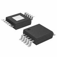
Available in 10-Pin MSOP or 14-Pin TSSOP
(PowerPAD)
−40°C to 85°C Ambient Temperature Range
Designed to meet USB 2.0 bus-powered hub
requirements, these devices also allow core and I/O
voltage sequencing in DSP applications, or power
segmentation in portable equipment. Each currentlimited switch is a 340-mΩ N-channel MOSFET capable
of supplying 200 mA of continuous current. A logic
enable compatible with 5-V logic and 3-V logic controls
each MOSFET as well as the LDO in the TPS2145. The
internal charge pump provides the gate drive controlling
the power-switch rise times and fall times, minimizing
current surges during switching. The charge pump
requires no external components.
APPLICATIONS
D USB Hubs and Peripherals
D
D
− Keyboards
− Zip Drives
− Speakers and Headsets
PDAs and Portable Electronics
DSP Power Sequencing
The LDO has a drop-out voltage of only 0.35 V and with
the independent enable on the TPS2145 LDO, the LDO
can be used as an additional switch. The LDO output
range for the TPS2145 is 1 V to 3.3 V, while the
TPS2147 is fixed at 3.3 V.
The TPS2145 and TPS2147 have active-low switch
enables and the TPS2155 and TPS2157 have
active-high switch enables.
LDO and dual switch family selection guide and schematics
VIN/SW1
LDO
LDO_OUT
LDO_OUT
VIN/SW1
OC1
OC1
LDO_EN
OUT1
OUT1
EN2
EN1
GND
VIN/SW1
LDO
TPS2149/59
MSOP−8
TPS2148/58
MSOP−8
TPS2147/57
MSOP−10
TPS2145/55
TSSOP−14
LDO
LDO_OUT
VIN
LDO
LDO_OUT
LDO_ADJ
LDO_EN
OUT2
EN1
EN1
EN1
OUT1
SW2
OUT2
SW2
OUT2
EN2
GND
OC2
EN2
GND
OC2
OUT1
OC
OUT2
EN2
GND
Please be aware that an important notice concerning availability, standard warranty, and use in critical applications of
Texas Instruments semiconductor products and disclaimers thereto appears at the end of this data sheet.
PowerPAD is a trademark of Texas Instruments.
���������� �
�
�������!��� �" #$��%�! �" �� &$'(�#�!��� )�!%*
���)$#!" #������ !� "&%#���#�!���" &%� !+% !%��" �� �%,�" ��"!�$�%�!"
"!��)��) -�����!.* ���)$#!��� &��#%""��/ )�%" ��! �%#%""���(. ��#($)%
!%"!��/ �� �(( &����%!%�"*
Copyright 2001, Texas Instruments Incorporated
www.ti.com
1
��������� ������
�������� ������
SLVS333 − AUGUST 2001
AVAILABLE OPTIONS
TA
−40°C to 85°C
PACKAGED DEVICES
PACKAGE
AND PIN
COUNT
DESCRIPTION
ACTIVE LOW
(SWITCH)
ACTIVE HIGH
(SWITCH)
Adjustable LDO with LDO enable
TSSOP-14
TPS2145IPWP
TPS2155IPWP
3.3-V fixed LDO
MSOP-10
TPS2147IDGQ
TPS2157IDGQ
3.3-V Fixed LDO with LDO enable and LDO output
switch
MSOP-8
TPS2148IDGN
TPS2158IDGN
3.3-V Fixed LDO, shared input with switches
MSOP-8
TPS2149IDGN
TPS2159IDGN
NOTE: All options available taped and reeled. Add an R suffix (e.g. TPS2145IPWPR)
TPS2145, TPS2155
TSSOP (PWP) PACKAGE
(TOP VIEW)
OUT1
VIN/SWIN1
SWIN2
LDO_OUT
OUT2
NC
LDO_ADJ
1
2
3
4
5
6
7
14
13
12
11
10
9
8
TPS2147, TPS2157
MSOP (DGQ) PACKAGE
(TOP VIEW)
EN1†
EN2†
OC1
OC2
LDO_EN
NC
GND
OUT1
VIN/SWIN1
SWIN2
LDO_OUT
OUT2
1
10
2
9
3
8
4
7
5
6
EN1†
EN2†
OC1
OC2
GND
† Pin 9 and 10 are active high for TPS2157.
NC − No internal connection
† Pin 13 and 14 are active high for TPS2155.
absolute maximum ratings over operating free-air temperature (unless otherwise noted)†
Input voltage range: VI(VIN/SWIN1), VI(SWIN2),VI(ENx), VI(LDO_EN) . . . . . . . . . . . . . . . . . . . . . . . . . . . . −0.3 V to 6 V
Output voltage range: VO(OUTx), VO(LDO_OUT), VO(OCx) . . . . . . . . . . . . . . . . . . . . . . . . . . . . . . . . . . . . −0.3 V to 6 V
Maximum output current, IO(OCx) . . . . . . . . . . . . . . . . . . . . . . . . . . . . . . . . . . . . . . . . . . . . . . . . . . . . . . . . . . . . . . ±10 mA
Continuous output current, IO(OUTx), IO(LDO_OUT) . . . . . . . . . . . . . . . . . . . . . . . . . . . . . . . . . . . . . . . . Internally limited
Continuous total power dissipation . . . . . . . . . . . . . . . . . . . . . . . . . . . . . . . . . . . . . . . . . . See Dissipation Rating Table
Operating virtual-junction temperature range, TJ . . . . . . . . . . . . . . . . . . . . . . . . . . . . . . . . . . . . . . . . . . −40°C to 110°C
Storage temperature range, Tstg . . . . . . . . . . . . . . . . . . . . . . . . . . . . . . . . . . . . . . . . . . . . . . . . . . . . . . . . −65°C to 150°C
Lead temperature soldering 1,6 mm (1/16 inch) from case for 10 seconds . . . . . . . . . . . . . . . . . . . . . . . . . . . . 260°C
Electrostatic discharge (ESD) protection: Human body model . . . . . . . . . . . . . . . . . . . . . . . . . . . . . . . . . . . . . . . . . 2 kV
Charged device model (CDM) . . . . . . . . . . . . . . . . . . . . . . . . . . . . . . . . 1 kV
† Stresses beyond those listed under “absolute maximum ratings” may cause permanent damage to the device. These are stress ratings only, and
functional operation of the device at these or any other conditions beyond those indicated under “recommended operating conditions” is not
implied. Exposure to absolute-maximum-rated conditions for extended periods may affect device reliability.
‡ All voltages are with respect to GND.
DISSIPATION RATING TABLE
2
PACKAGE
TA ≤ 25°C
POWER RATING
DERATING FACTOR
ABOVE TA = 25°C
TA = 70°C
POWER RATING
TA = 85°C
POWER RATING
MSOP10
1293.1 mW
17.2 mW/°C
517.2 mW
258.6 mW
PWP14
2000 mW
26.6 mW/°C
800 mW
400 mW
www.ti.com
��������� ������
�������� ������
SLVS333 − AUGUST 2001
recommended operating conditions
VI(VIN/SWIN1)
VI(SWIN2)
Input voltage
VI(ENx)
VI(LDO_EN)
Continuous output current, IO
Output current limit, IO(LMT)
MIN
MAX
2.9
5.5
2.9
5.5
0
5.5
0
V
5.5
LDO_OUT
200
OUT1, OUT2
150
LDO_OUT
275
550
OUT1, OUT2
200
400
−40
100
Operating virtual-junction temperature range, TJ
UNIT
mA
mA
°C
electrical characteristics over recommended operating junction-temperature range,
2.9 V ≤ VI(VIN/SWIN1) ≤ 5.5 V, 2.9 V ≤ VI(SWIN2) ≤ 5.5 V, TJ = −40°C to 100°C (unless otherwise noted)
general
PARAMETER
TEST CONDITIONS
Off-state supply current
VI(VIN/SWIN1) = 5 V,
VI(SWIN2) = 5 V
Forward leakage current
II
Total input current at VIN/SWIN1
and SWIN2
VI(VIN/SWIN1) = 5 V,
VI(SWIN2) = 5 V,
No load on OUTx,
No load on LDO_OUT
VI(ENx) = 5 V (inactive),
VI(LDO_EN) = 0 V (inactive),
VO(LDO_OUT) = no load,
VO(OUTx) = no load
VI(ENx) = 5 V (inactive),
VI(LDO_EN) = 0 V (inactive),
VO(LDO_OUT) = 0 V,
VO(OUTx) = 0 V
(measured from outputs to
ground)
MIN
TYP
MAX
UNIT
20
µA
1
µA
VI(LDO_EN) = 5 V (active),
VI(ENx) = on (active)
150
µA
VI(LDO_EN) = 0 V (inactive),
VI(ENx) = on (active)
100
µA
VI(LDO_EN) = 5 V (active),
VI(ENx) = off (inactive)
100
µA
www.ti.com
3
��������� ������
�������� ������
SLVS333 − AUGUST 2001
electrical characteristics over recommended operating junction-temperature range,
2.9 V ≤ VI(VIN/SWIN1) ≤ 5.5 V, 2.9 V ≤ VI(SWIN2) ≤ 5.5 V, VI(ENx) = 0 V or VI(ENx) = 5 V,
VI(LDO_EN) = 5 V, TJ = −40°C to 100°C (unless otherwise noted)
power switches
PARAMETER
rDS(on)
Ilkg(R)
IOS
Static drain-source on-state resistance,
VIN/SWIN1 or SWIN2 to OUTx
Reverse leakage current at OUTx
TEST CONDITIONS
MIN
TYP
TJ = −40°C to 100°C,
IO(LDO_OUT) = 200 mA,
IOUT1 and IOUT2 = 150 mA
UNIT
580
mΩ
TJ = 25°C,
IO(LDO_OUT) = 200 mA,
IOUT1 and IOUT2 = 150 mA
VO(OUTx) = 5 V,
LDO_EN = don’t care
MAX
340
VI(ENx) = 5 V,
VI(ENx) = 0 V,
SWIN2 floating,
VI(VIN/SWIN1) = 5 V
VI(ENx) = 5 V,
VI(ENx) = 0 V,
VI(SWIN2) = 0,
VI(VIN/SWIN1) = 2.9 V
VI(ENx) = 5 V,
VI(ENx) = 0 V,
VI(SWIN2) = 0,
VI(VIN/SWIN1) = 0 V
10
10
µA
10
Short circuit output current
OUTx connected to GND, device enabled into short
circuit
Delay time for asserting OC flag
From IOUTx at 95% of current limit level to 50% OC
5.5
ms
Delay time for deasserting OC flag
From IOUTx at 95% of current limit level to 50% OC
10.5
ms
0.2
0.4
A
timing parameters, power switches
PARAMETER
ton
Turnon time, OUTx switch, (see Note 1)
toff
Turnoff time, OUTx switch (see Note 1)
tr
Rise time, OUTx switch (see Note 1)
tf
Fall time, OUTx switch (see Note 1)
TEST CONDITIONS
CL = 100 µF
CL = 1 µF
CL = 100 µF
CL = 1 µF
CL = 100 µF
CL = 1 µF
CL = 100 µF
CL = 1 µF
RL = 33 Ω
RL = 33 Ω
RL = 33 Ω
RL = 33 Ω
MIN
TYP
0.5
MAX
UNIT
6
0.1
3
5.5
12
0.05
4
0.5
5
0.1
2
5.5
9
0.05
1.2
ms
NOTE 1. Specified by design, not tested in production.
undervoltage lockout at VIN/SWIN1
PARAMETER
TEST CONDITIONS
UVLO Threshold
MIN
Hysteresis (see Note 1)
Deglitch (see Note 1)
50
www.ti.com
MAX
2.85
260
NOTE 1. Specified by design, not tested in production.
4
TYP
2.2
UNIT
V
mV
µs
��������� ������
�������� ������
SLVS333 − AUGUST 2001
electrical characteristics over recommended operating junction-temperature range,
2.9 V ≤ VI(VIN/SWIN1) ≤ 5.5 V, 2.9 V ≤ VI(SWIN2) ≤ 5.5 V, VI(ENx) = 0 V or VI(ENx) = 5 V,
VI(LDO_EN) = 5 V, TJ = −40°C to 100°C (unless otherwise noted) (continued)
undervoltage lockout at SWIN2
PARAMETER
TEST CONDITIONS
UVLO Threshold
MIN
TYP
MAX
2.2
Hysteresis (see Note 1)
2.85
260
Deglitch (see Note 1)
UNIT
V
mV
µs
50
NOTE 1. Specified by design, not tested in production.
electrical characteristics over recommended operating junction-temperature range,
2.9 V ≤ VI(VIN/SWIN1) ≤ 5.5 V, 2.9 V ≤ VI(SWIN2) ≤ 5.5 V, VI(ENx) = 0 V or VI(ENx) = 5 V,
VI(LDO_EN) = 5 V, CL(LDO_OUT) = 10 µF, TJ = −40°C to 100°C (unless otherwise noted)
fixed-voltage regulator, 3.3 V
PARAMETER
VO
Output voltage, dc
Dropout voltage
Line regulation voltage (see Note 1)
IOS
Ilkg(R)
TEST CONDITIONS†
VI(VIN/SWIN1) = 4.25 V to 5.25 V,
IO(LDO_OUT) = 0.5 mA to 200 mA
TYP
MAX
UNIT
3.20
3.3
3.40
V
0.35
V
0.1
%/V
VI(VIN/SWIN1) = 3.2 V,
IO(LDO_OUT) = 200 mA,
IO(OUT1) = 150 mA
VI(VIN/SWIN1) = 4.25 V to 5.25 V,
IO(LDO_OUT) = 5 mA
Load regulation voltage (see Note 1)
VI(VIN/SWIN1) = 4.25 V,
IO(LDO_OUT) = 5 mA to 200 mA
Short-circuit current limit
VI(VIN/SWIN1) = 4.25 V,
LDO_OUT connected to GND
Reverse leakage current into
LDO_OUT
MIN
0.275
0.4%
1.15%
0.33
0.55
A
VO(LDO_OUT) = 3.3 V,
VI(VIN/SWIN1) = 0 V,
VI(LDO_EN) = 0 V
10
µA
VO(LDO_OUT) = 5.5 V,
VI(VIN/SWIN1) = 2.9 V,
VI(LDO_EN) = 0 V
10
µA
ton
Turnoff time, LDO_EN
transitioning low (see Note 1)
RL = 16 Ω, CL(LDO_OUT) = 10 µF
0.25
1
ms
toff
Turnon time, LDO_EN
transitioning high (see Note 1)
RL = 16 Ω, CL(LDO_OUT) = 10 µF
0.1
1
ms
0.1
1
ms
Ramp-up time, LDO_OUT (0% to 90%)
Power supply rejection
VI(LDO_EN) = 5 V, VIN/SWIN1 ramping up from 10%
to 90% in 0.1 ms, RL = 16 Ω,
CL(LDO_OUT) = 10 µF
f = 1 kHz, CL(LDO_OUT) = 4.7 µF,
ESR = 0.25 Ω, IO = 5 mA,
VI(VIN/SWIN1)p−p = 100 mV
50
dB
† Pulse-testing techniques maintain junction temperature close to ambient temperature; thermal effects must be taken into account separately.
NOTE 1. Specified by design, not tested in production.
www.ti.com
5
��������� ������
�������� ������
SLVS333 − AUGUST 2001
electrical characteristics over recommended operating junction-temperature range,
2.9 V ≤ VI(VIN/SWIN1) ≤ 5.5 V, 2.9 V ≤ VI(SWIN2) ≤ 5.5 V, VI(ENx) = 0 V or VI(ENx) = 5 V,
VI(LDO_EN) = 5 V, CL(LDO_OUT) = 10 µF, TJ = −40°C to 100°C (unless otherwise noted) (continued)
adjustable voltage regulator (Vx = 1 V to 3.3 V)
PARAMETER
VO
Output voltage, dc (see Note 2)
Dropout voltage (VIN/SWIN1 to LDO_OUT)
Line regulation voltage (see Note 1)
Load regulation voltage (see Note 1)
IOS
Ilkg(R)
Short-circuit current limit
Reverse leakage current into LDO_OUT
TEST CONDITIONS†
VI(VIN/SWIN1) =Vx + 0.6 V to 5.5 V and
VI(VIN/SWIN1) > 2.9 V,
IO = 0.5 mA to 200 mA
VI(VIN/SWIN1) = Vx − 0.1 V, IO = 200 mA
MIN
TYP
MAX
0.97Vx
Vx
1.03Vx
V
0.5
V
0.1
%/V
VI(VIN/SWIN1) = Vx + 0.6 V to 5.5 V and
VI(VIN/SWIN1) > 2.9 V,
IO = 5 mA
VI(VIN/SWIN1) = Vx + 0.6 V to 5.5 V and
VI(VIN/SWIN1) > 2.9 V,
IO = 5 mA to 200 mA
VI(VIN/SWIN1) = Vx + 0.6 V to 5.5 V and
VI(VIN/SWIN1) > 2.9 V,
LDO_OUT connected to GND
0.275
0.4%
1%
0.33
0.575
UNIT
A
VO(LDO_OUT) = Vx,
VI(VIN/SWIN1) = 0 V,
VI(LDO_EN) = 0 V
10
µA
VO(LDO_OUT) = 5.5 V,
VI(VIN/SWIN1) = 2.8 V,
VI(LDO_EN) = 0 V
10
µA
ton
Turnoff time, LDO_EN
transitioning low (see Note 1)
From 50% LDO_EN to 10% LDO_OUT,
RL = Vx/0.2 Ω, CL(LDO_OUT) = 10 µF
0.1
1
ms
toff
Turnon time, LDO_EN
transitioning high (see Note 1)
From 50% LDO_EN to 90% LDO_OUT,
RL = Vx/0.2 Ω, CL(LDO_OUT) = 10 µF
0.1
1
ms
Ramp-up time, LDO_OUT (0% to 90%)
VI(LDO_EN) = 5 V, VIN/SWIN1 ramping up
from 10% to 90% in 0.1 ms, RL = Vx/0.2 Ω,
CL(LDO_OUT) = 10 µF
0.1
1
ms
Output tracking
OUT1 lag time from LDO_OUT given
LDO_EN and EN1 have been asserted simultaneously to turnon their respective outputs. Measured at 1 V. (see Note 1)
LDO load RL = Vx/0.2 Ω,
CL(LDO_OUT) = 10 µF,
OUT1 RL = 33 Ω, 10 µF,
VI(VIN/SWIN1) = 3.3 V
0
1
ms
f = 1 kHz, CL(LDO_OUT) = 4.7 µF,
ESR = 0.25 Ω, IO = 5 mA,
50
dB
VI(VIN/SWIN1)p−p = 100 mV
† Pulse-testing techniques maintain junction temperature close to ambient temperature; thermal effects must be taken into account separately.
NOTES: 1. Specified by design, not tested in production.
2. Does not include error introduced by external resistive divider R1, R2 tolerance.
Power supply rejection
6
www.ti.com
��������� ������
�������� ������
SLVS333 − AUGUST 2001
electrical characteristics over recommended operating junction-temperature range,
2.9 V ≤ VI(VIN/SWIN1) ≤ 5.5 V, 2.9 V ≤ VI(SWIN2) ≤ 5.5 V, VI(ENx) = 0 V or VI(ENx) = 5 V,
VI(LDO_EN) = 5 V, TJ = −40°C to 100°C (unless otherwise noted)
enable input, ENx (active low)
PARAMETER
VIH
VIL
High-level input voltage
II
Input current, pullup (source)
TEST CONDITIONS
MIN
TYP
MAX
2
UNIT
V
Low-level input voltage
VI(ENx) = 0 V
0.8
V
5
µA
enable input, ENx (active high)
PARAMETER
VIH
VIL
High-level input voltage
II
Input current, pulldown (sink)
TEST CONDITIONS
MIN
TYP
MAX
2
UNIT
V
Low-level input voltage
VI(ENx) = 5 V
0.8
V
5
µA
enable input, LDO_EN (active high)
PARAMETER
VIH
VIL
High-level input voltage
II
Input current, pulldown
TEST CONDITIONS
MIN
TYP
MAX
2
V
Low-level input voltage
VI(LDO_EN) = 5 V
Falling-edge deglitch (see Note 1)
UNIT
0.8
V
5
µA
µs
50
NOTE 1. Specified by design, not tested in production.
logic output, OCx
PARAMETER
TEST CONDITIONS
Current sinking at VO = 0.4 V
MIN
TYP
MAX
1
UNIT
mA
thermal shutdown characteristics
PARAMETER
First thermal shutdown (shuts down switch or regulator
in overcurrent)
TEST CONDITIONS
Occurs at or above specified temperature
when overcurrent is present.
Recovery from thermal shutdown
Second thermal shutdown (shuts down all switches and
regulator)
MIN
TYP
Second thermal shutdown hysteresis
UNIT
120
110
Occurs on rising temperature, irrespective of
overcurrent.
MAX
°C
155
10
www.ti.com
7
��������� ������
�������� ������
SLVS333 − AUGUST 2001
TPS2145 functional block diagram
1 V to 3.3 V / 200 mA
LDO
VIN/SWIN1
LDO_OUT
LDO_ADJ
LDO_EN
CS
Charge
Pump
Driver
OUT1
Current
Limit
OC1
EN1
Thermal
Sense
CS
SWIN2
Driver
OUT2
Current
Limit
OC2
EN2
Thermal
Sense
GND
TPS2147 functional block diagram
3.3 V / 200 mA
LDO
VIN/SWIN1
LDO_OUT
CS
Charge
Pump
Driver
OUT1
Current
Limit
OC1
EN1
Thermal
Sense
SWIN2
CS
Driver
8
Current
Limit
OC2
EN2
GND
OUT2
Thermal
Sense
www.ti.com
��������� ������
�������� ������
SLVS333 − AUGUST 2001
Terminal Functions
TERMINAL
NO.
NAME
PWP-14
TPS2145
EN1
TPS2155
TPS2147
14
EN1
14
EN2
13
GND
8
DESCRIPTION
TPS2157
10
I
Logic level enable to transfer power to OUT1
9
I
Logic level enable to transfer power to OUT2
10
13
EN2
I/O
DGQ-10
9
8
6
6
Ground
LDO_ADJ
7
7
I
User feedback for adjustable regulator
LDO_EN
10
10
I
Logic level LDO enable. Active high.
LDO output
LDO_OUT
4
4
NC
6, 9
6, 9
4
4
O
OC1
12
12
8
8
O
Overcurrent status flag for OUT1. Open-drain output.
OC2
OUT1
11
11
7
7
O
Overcurrent status flag for OUT2. Open-drain output.
1
1
1
1
O
Switch 1 output
OUT2
5
5
5
5
SWIN2
3
3
3
3
I
Input for switch 2
VIN/SWIN1
2
2
2
2
I
Input for LDO and switch 1; device supply voltage
No connection
Switch 2 output
detailed description
VIN/SWIN1
The VIN/SWIN1 serves as the input to the internal LDO and as the input to one N-channel MOSFET. The fixed
or adjustable LDO has a dropout voltage of 0.35 V and is rated for 200 mA of continuous current. The power
switch is an N-channel MOSFET with a maximum on-state resistance of 580 mΩ. Configured as a high-side
switch, the power switch prevents current flow from OUT to IN and IN to OUT when disabled. The power switch
is rated at 200 mA, continuous current. VIN/SWIN1 must be connected to a voltage source for device operation.
SWIN2
SWIN2 is the input to the other N-channel MOSFET, which also has a maximum on-state resistance of 580 mΩ.
Configured as a high-side switch, the power switch prevents current flow from OUT to IN and IN to OUT when
disabled. The power switch is rated at 200 mA, continuous current.
OUTx
OUT1 and OUT2 are the outputs from the internal power-distribution switches.
LDO_OUT
LDO_OUT is the output of the internal 200-mA LDO. The fixed version of the LDO has an output of 3.3 V. The
adjustable version has an output voltage range of 1 V to 3.3 V.
LDO_ADJ
This input only applies to the adjustable LDO version of this device (TPS2145/55). LDO_ADJ is used to adjust
the output voltage anywhere between 1 V and 3.3 V.
LDO_EN
The active high input, LDO_EN, only applies to the adjustable LDO version of this device (TPS2145/55).
LDO_EN is used to enable the internal LDO and is compatible with TTL and CMOS logic.
www.ti.com
9
��������� ������
�������� ������
SLVS333 − AUGUST 2001
detailed description (continued)
enable (ENx, ENx)
The logic enable disables the power switch. Both switches have independent enables and are compatible with
both TTL and CMOS logic.
overcurrent (OCx)
The OCx open-drain output is asserted (active low) when an overcurrent condition is encountered. The output
will remain asserted until the overcurrent condition is removed.
current sense
A sense FET monitors the current supplied to the load. Current is measured more efficiently by the sense FET
than by conventional resistance methods. When an overload or short circuit is encountered, the current-sense
circuitry sends a control signal to the driver. The driver in turn reduces the gate voltage and drives the power
FET into its saturation region, which switches the output into a constant-current mode and holds the current
constant while varying the voltage on the load.
thermal sense
A dual-threshold thermal trip is implemented to allow fully independent operation of the power distribution
switches. In an overcurrent or short-circuit condition, the junction temperature rises. When the die temperature
rises to approximately 120°C, the internal thermal sense circuitry determines which power switch is in an
overcurrent condition and turns off that switch, thus isolating the fault without interrupting operation of the
adjacent power switch. Because hysteresis is built into the thermal sense, the switch turns back on after the
device has cooled approximately 10 degrees. The switch continues to cycle off and on until the fault is removed.
undervoltage lockout
A voltage sense circuit monitors the input voltage. When the input voltage is below approximately 2.5 V, a control
signal turns off the power switch.
PARAMETER MEASUREMENT INFORMATION
Current
Meter
DUT
IN
OUT
A
+
Figure 1. Current Limit Test Circuit
10
www.ti.com
��������� ������
�������� ������
SLVS333 − AUGUST 2001
PARAMETER MEASUREMENT INFORMATION
50%
VI(ENx)
50%
tpd(off)
ton
toff
tpd(on)
90%
VO(OUTx)
90%
10%
10%
tr
tf
90%
VO(OUTx)
90%
10%
10%
TIMING
Figure 2. Timing and Internal Voltage Regulator Transition Waveforms
TYPICAL CHARACTERISTICS
SWITCH TURNON DELAY AND RISE TIME
WITH 1-µF LOAD
SWITCH TURNOFF DELAY AND FALL TIME
WITH 1-µF LOAD
VI(EN)
(5 V/div)
VI(EN)
(5 V/div)
VO(OUT)
(2 V/div)
VO(OUT)
(2 V/div)
VI = 5 V
TA = 25°C
CL = 1 µF
RL = 25 Ω
VI = 5 V
TA = 25°C
CL = 1 µF
RL = 25 Ω
0
0.4
0.8 1.2
1.6 2 2.4 2.8
t − Time − ms
3.2
3.6
4.2
Figure 3
0
0.4
0.8 1.2
1.6 2 2.4 2.8
t − Time − ms
3.2
3.6
4.2
Figure 4
www.ti.com
11
��������� ������
�������� ������
SLVS333 − AUGUST 2001
TYPICAL CHARACTERISTICS
SWITCH TURNOFF DELAY AND FALL TIME
WITH 120-µF LOAD
SWITCH TURNON DELAY AND RISE TIME
WITH 120-µF LOAD
VI(EN)
(5 V/div)
VI(EN)
(5 V/div)
VO(OUT)
(2 V/div)
VO(OUT)
(2 V/div)
VI = 5 V
TA = 25°C
CL = 120 µF
RL = 25 Ω
VI = 5 V
TA = 25°C
CL = 120 µF
RL = 25 Ω
0
2
4
6
8 10 12 14
t − Time − ms
16
18
0
20
4
Figure 5
8
12
16 20 24 28
t − Time − ms
32
36
40
Figure 6
LDO TURNON DELAY AND RISE TIME
WITH 4.7-µF LOAD
SHORT-CIRCUIT CURRENT, SWITCH
ENABLED INTO A SHORT
VI(EN)
(5 V/div)
VI = 5 V
TA = 25°C
CL = 4.7 µF
RL = 13.2 Ω
VI(LDO_EN)
(5 V/div)
VO(LDO_OUT)
(1 V/div
IO(OUT)
(100 mA/div)
0
1
2
3
4
5
6
t − Time − ms
7
8
9
10
Figure 7
12
0
0.4
0.8 1.2
1.6 2 2.4 2.8
t − Time − ms
Figure 8
www.ti.com
3.2
3.6 4.2
��������� ������
�������� ������
SLVS333 − AUGUST 2001
TYPICAL CHARACTERISTICS
LINE TRANSIENT RESPONSE
LOAD TRANSIENT RESPONSE
IO(LDO_OUT)
5.25 V
VI(VIN)
4.25 V
(200 mA/div)
∆VO(LDO_OUT)
(100 mV/div)
∆VO(LDO_OUT)
(0.05 V/div)
TA = 25°C
CL(LDO_OUT) = 4.7 µF
ESR = 1 Ω
IO(LDO_OUT) = 200 mA
0
TA = 25°C
CL(LDO_OUT) = 4.7 µF
ESR = 1 Ω
100 200 300 400 500 600 700 800 900 1000
t − Time − µs
0
100 200 300 400 500 600 700 800 900 1000
t − Time − µs
Figure 10
Figure 9
SUPPLY CURRENT
vs
SUPPLY VOLTAGE
140
140
120
120
I DD − Supply Current − µ A
I DD − Supply Current − µ A
SUPPLY CURRENT
vs
JUNCTION TEMPERATURE
100
80
60
40
80
60
40
20
20
0
−40
100
−20
0
20
40
60
80
100
TJ − Temperature − °C
Figure 11
0
2.5
3
3.5
4
4.5
VCC − Supply Voltage − V
5
5.5
Figure 12
www.ti.com
13
��������� ������
�������� ������
SLVS333 − AUGUST 2001
rDS(on) − Static Drain-Source On-State Resistance − Ω
STATIC DRAIN-SOURCE ON-STATE RESISTANCE
vs
JUNCTION TEMPERATURE
0.6
0.55
0.5
0.45
SW1
0.4
SW2
0.35
0.3
0.25
0.2
0.15
0.1
−40
−20
0
20
40
60
80
TJ − Junction Temperature − °C
100
rDS(on) − Static Drain-Source On-State Resistance − Ω
TYPICAL CHARACTERISTICS
STATIC DRAIN-SOURCE ON-STATE RESISTANCE
vs
SUPPLY VOLTAGE
0.38
0.37
0.36
0.35
SW1
0.34
SW2
0.33
0.32
0.31
0.3
2.5
3
Figure 13
380
380
360
360
Short Circuit Current − mA
Short Circuit Current − mA
400
340
320
SW1
280
SW2
260
5.5
320
SW1
300
280
220
220
0
20
40
60
80
TJ − Free-Air Temperature − °C
100
SW2
260
240
Figure 15
14
5
340
240
−20
5.5
SHORT CIRCUIT CURRENT
vs
SUPPLY VOLTAGE
400
200
−40
5
Figure 14
SHORT CIRCUIT CURRENT
vs
JUNCTION TEMPERATURE
300
3.5
4
4.5
VCC − Supply Voltage
200
2.5
3
3.5
4
4.5
VCC − Supply Voltage
Figure 16
www.ti.com
��������� ������
�������� ������
SLVS333 − AUGUST 2001
TYPICAL CHARACTERISTICS
UNDERVOLTAGE LOCKOUT
vs
JUNCTION TEMPERATURE
2.9
UVLO − Undervoltage Lockout − V
2.8
Rising
2.7
2.6
2.5
Falling
2.4
2.3
2.2
2.1
−40 −25 −10
5 20 35 50 65 80
TJ − Junction Temperature − °C
95 110
Figure 17
APPLICATION INFORMATION
external capacitor requirements on power lines
Ceramic bypass capacitors (0.01-µ to 0.1-µ) between VIN/SWIN1 and GND and SWIN2 and GND, close to the
device, are recommended to improve load transient response and noise rejection.
Bulk capacitors ( 4.7-µF) between VIN/SWIN1 and GND and between SWIN2 and GND are also recommended,
especially if load transients in the hundreds of milliamps with fast rise times are anticipated.
A 66-µF bulk capacitor is recommended from OUTx to ground, especially when the output load is heavy. This
precaution helps reduce transients seen on the power rails. Additionally, bypassing the outputs with a 0.1-µF
ceramic capacitor improves the immunity of the device to short-circuit transients.
LDO output capacitor requirements
Stabilizing the internal control loop requires an output capacitor connected between LDO_OUT and GND. The
minimum recommended capacitance is a 4.7 µF with an ESR value between 200 mΩ and 10 Ω. Solid tantalum
electrolytic, aluminum electrolytic and multilayer ceramic capacitors are all suitable, provided they meet the
ESR requirements.
The adjustable LDO (for voltages lower than 3 V) requires a bypass capacitor across the feedback resistor as
shown in Figure 18. The value of this capacitor is determined by using the following equation:
Cf +
1
(63.7e 3
2
3.14
R1)
* 4 pf
(1)
where R1 is derived by programming the adjustable LDO (see programming the adjustable LDO regulator
section shown below).
www.ti.com
15
��������� ������
�������� ������
SLVS333 − AUGUST 2001
APPLICATION INFORMATION
programming the adjustable LDO regulator
The output voltage of the TPS2145 adjustable regulator is programmed using an external resistor divider as
shown in Figure 18. The output voltage is calculated using:
ǒ
Ǔ
LDO_OUT + V ref 1) R1
R2
(2)
where Vref = 0.8 V typical (internal reference voltage).
Resistors R1 and R2 should be chosen for approximately 4-µA (minimum) divider current. Lower value resistors
can be used but offer no inherent advantage and waste more power. Higher values should be avoided as a
minimum load is required to sink the LDO forward leakage and maintain regulation. The recommended design
procedure is to choose R2 = 200 kΩ to set the divider current at 4-µA and then solve the LDO_OUT equation
for R1.
TPS2145
VIN/SWIN1 LDO_OUT
0.1 µF
R1
4.7 µF
LDO_EN
Cf
0.1 µF
10 µF
LDO_ADJ
R2
GND
Figure 18. External Resistor Divider
OUTPUT VOLTAGE PROGRAMMING GUIDE
OUTPUT VOLTAGE
R1
R2
Cfb
3.3
625 kΩ
200 kΩ
3.0
550 kΩ
200 kΩ
NR†
NR†
2.5
425 kΩ
200 kΩ
2 pf
1.8
250 kΩ
200 kΩ
6 pf
1.5
175 kΩ
200 kΩ
10.3 pf
1.0
50 kΩ
200 kΩ
46 pf
† NR − Not required
overcurrent
A sense FET is used to measure current through the device. Unlike current-sense resistors, sense FETs do not
increase the series resistance of the current path. When an overcurrent condition is detected, the device
maintains a constant output current. Complete shutdown occurs only if the fault is present long enough to
activate thermal limiting.
Three possible overload conditions can occur. In the first condition, the output is shorted before the device is
enabled or before VIN has been applied. The TPS2145 and TPS2147 sense the short and immediately switch
to a constant-current output.
In the second condition, the short occurs while the device is enabled. At the instant the short occurs, very high
currents may flow for a very short time before the current-limit circuit can react. After the current-limit circuit has
tripped (reached the overcurrent trip threshold), the device switches into constant-current mode.
16
www.ti.com
��������� ������
�������� ������
SLVS333 − AUGUST 2001
APPLICATION INFORMATION
overcurrent (continued)
In the third condition, the load has been gradually increased beyond the recommended operating current. The
current is permitted to rise until the current-limit threshold is reached or until the thermal limit of the device is
exceeded. The TPS2145 and TPS2147 are capable of delivering current up to the current-limit threshold without
damaging the device. Once the threshold has been reached, the device switches into its constant-current mode.
OC response
The OCx open-drain output is asserted (active low) when an overcurrent condition is encountered. The output
will remain asserted until the overcurrent condition is removed. Connecting a heavy capacitive load to an
enabled device can cause momentary false overcurrent reporting from the inrush current flowing through the
device, charging the downstream capacitor. The TPS2145 and TPS2147 are designed to reduce false
overcurrent reporting. An internal overcurrent transient filter eliminates the need for external components to
remove unwanted pulses. Using low-ESR electrolytic capacitors on OUTx lowers the inrush current flow through
the device during hot-plug events by providing a low-impedance energy source, also reducing erroneous
overcurrent reporting.
power dissipation and junction temperature
The major source of power dissipation for the TPS2145 and TPS2147 comes from the internal voltage regulator
and the N-channel MOSFETs. Checking the power dissipation and junction temperature is always a good
design practice and it starts with determining the rDS(on) of the N-channel MOSFET according to the input
voltage and operating temperature. As an initial estimate, use the highest operating ambient temperature of
interest and read rDS(on) from the graphs shown in the Typical Characteristics section of this data sheet. Using
this value, the power dissipation per switch can be calculated using:
P D + r DS(on)
I2
(3)
Multiply this number by two to get the total power dissipation coming from the N-channel MOSFETs.
The power dissipation for the internal voltage regulator is calculated using:
ǒ
P D + V –V
I O(min)
Ǔ
I
O
(4)
The total power dissipation for the device becomes:
P D(total) + P
D(voltage regulator)
ǒ
) 2
P
D(switch)
Ǔ
(5)
Finally, calculate the junction temperature:
TJ + PD
R qJA ) T A
(6)
Where:
TA = Ambient Temperature °C
RθJA = Thermal resistance °C/W, equal to inverting the derating factor found on the power dissipation table
in this data sheet.
Compare the calculated junction temperature with the initial estimate. If they do not agree within a few degrees,
repeat the calculation, using the calculated value as the new estimate. Two or three iterations are generally
sufficient to get a reasonable answer.
www.ti.com
17
��������� ������
�������� ������
SLVS333 − AUGUST 2001
APPLICATION INFORMATION
thermal protection
Thermal protection prevents damage to the IC when heavy-overload or short-circuit faults are present for
extended periods of time. The faults force the TPS2145 and TPS2147 into constant-current mode at first, which
causes the voltage across the high-side switch to increase; under short-circuit conditions, the voltage across
the switch is equal to the input voltage. The increased dissipation causes the junction temperature to rise to high
levels.
The protection circuit senses the junction temperature of the switch and shuts it off. Hysteresis is built into the
thermal sense circuit, and after the device has cooled approximately 10 degrees, the switch turns back on. The
switch continues to cycle in this manner until the load fault or input power is removed.
The TPS2145 and TPS2147 implement a dual thermal trip to allow fully independent operation of the power
distribution switches. In an overcurrent or short-circuit condition, the junction temperature will rise. Once the die
temperature rises to approximately 120°C, the internal thermal-sense circuitry checks to determine which
power switch is in an overcurrent condition and turns that power switch off, thus isolating the fault without
interrupting operation of the adjacent power switch. Should the die temperature exceed the first thermal trip
point of 120°C and reach 155°C, the device will turn off.
undervoltage lockout (UVLO)
An undervoltage lockout ensures that the device (LDO and switches) is in the off state at power up. The UVLO
will also keep the device from being turned on until the power supply has reached the start threshold (see
undervoltage lockout table), even if the switches are enabled. The UVLO will also be activated whenever the
input voltage falls below the stop threshold as defined in the undervoltage lockout table. This function facilitates
the design of hot-insertion systems where it is not possible to turn off the power switches before input power
is removed. Upon reinsertion, the power switches will be turned on with a controlled rise time to reduce EMI and
voltage overshoots.
universal serial bus (USB) applications
The universal serial bus (USB) interface is a multiplexed serial bus operating at either 12-Mb/s, or 1.5-Mb/s for
USB 1.1, or 480 Mb/s for USB 2.0. The USB interface is designed to accommodate the bandwidth required by
PC peripherals such as keyboards, printers, scanners, and mice. The four-wire USB interface was conceived
for dynamic attach-detach (hot plug-unplug) of peripherals. Two lines are provided for differential data, and two
lines are provided for 5-V power distribution.
USB data is a 3.3-V level signal, but power is distributed at 5 V to allow for voltage drops in cases where power
is distributed through more than one hub across long cables. Each function must provide its own regulated 3.3-V
from the 5-V input or its own internal power supply.
The USB specification defines the following five classes of devices, each differentiated by power-consumption
requirements:
D
D
D
D
D
Hosts/self-powered hubs (SPH)
Bus-powered hubs (BPH)
Low-power, bus-powered functions
High-power, bus-powered functions
Self-powered functions
The TPS2145 and TPS2147 are well suited for USB hub and peripheral applications. The internal LDO can be
used to provide the 3.3-V power needed by the controller while the dual switches distribute power to the
downstream functions.
18
www.ti.com
��������� ������
�������� ������
SLVS333 − AUGUST 2001
APPLICATION INFORMATION
USB power-distribution requirements
USB can be implemented in several ways, and, regardless of the type of USB device being developed, several
power-distribution features must be implemented.
D Hosts/self-powered hubs must:
−
−
Current-limit downstream ports
Report overcurrent conditions on USB VBUS
D Bus-powered hubs must:
−
−
−
Enable/disable power to downstream ports
Power up at


 工商网监
湘ICP备2023018690号
工商网监
湘ICP备2023018690号
