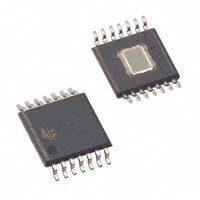
�������� �������
����� �� ����� �
SLVS399A − JANUARY 2002 − REVISED MAY 2006
��
��
��� ���
�� ������ ���� �
� �
����� ����� ���
�� ���������� ��������
� ����� �
�
������
FEATURES
D Complete Power Management Solution for
D
D
D
D
D
D
D
D
D
D
DESCRIPTION
The TPS2140/41/50/51 is a USB 1.0 and 2.0
Specification-compatible IC containing a dual-currentlimiting power switch and an adjustable low dropout
regulator (LDO). Both the switch and LDO limit inrush
current by controlling the turnon slew rate. The unique
dual-current-limiting feature of the switch allows USB
peripherals to utilize high-value capacitance at the
output of the switch, while keeping the inrush current
low. During turnon, the switch limits the current
delivered to the capacitive load to less than 100 mA.
When the output voltage from the switch reaches about
93% of the input voltage, the switch power good output
goes high, and the switch current limit increases to
800mA (minimum), at which point higher current loads
can be turned on. The higher current limit provides short
circuit protection while allowing the peripheral to draw
maximum current from the USB bus.
USB High-Power Peripherals
250 mA Low-Dropout Regulator (LDO) With
Enable and 325 mA (Typ) Current Limit
LDO Supports 2.7 V to 5.5 V VIN and 0.9 V to
3.3 V Adjustable VOUT
40 mΩ (Typ) High-Side MOSFET With Dual
Current Limit
Undervoltage Lockout and Power Good for
LDO and Switch
CMOS- and TTL-Compatible Enable Inputs
85 µA (Typ) Supply Current
5 µA (Typ) Standby Supply Current
Available in 14-Pin HTSSOP (PowerPAD)
−40°C to +85°C Ambient Temperature Range
Alternative to TPS2148/58 3.3-V LDO With
3.3-V Switch and 5-V Switch
The switch and LDO function independently, providing
flexibility in DSP applications requiring separate core
and I/O voltages. For example, in a DSP application
operating from a 3.3-V rail, the LDO can supply the DSP
core voltage down to 0.9 V, while the switch powers the
3.3-V (typical) DSP I/O supply. If supply sequencing is
required, the LDO power good output can be used to
enable the switch.
APPLICATIONS
D High-Power USB Peripherals
D
− ADSL Modems
− Digital Still and PC Cameras
− Zip Drives
− Speakers
DSP Sequencing
AVAILABLE OPTIONS
TA
−40°C to 85°C
PACKAGED DEVICES
PACKAGE
AND PIN
COUNT
ACTIVE LOW
(SWITCH)
ACTIVE HIGH
(SWITCH)
DSP
HTSSOP-14
TPS2140IPWP
TPS2150IPWP
USB
HTSSOP-14
TPS2141IPWP
TPS2151IPWP
DESCRIPTION
TARGET
APPLICATION
Adjustable LDO and 3.3 V switch with dual current
limit
Adjustable LDO and 5 V switch with dual current
limit
NOTE: All options available taped and reeled. Add an R suffix (e.g., TPS2140IPWPR)
Please be aware that an important notice concerning availability, standard warranty, and use in critical applications of
Texas Instruments semiconductor products and disclaimers thereto appears at the end of this data sheet.
PowerPAD is a trademark of Texas Instruments. USB is a trademark of Universal Serial Bus Association.
All other trademarks are the property of their respective owners.
����
����� �
�
����!"#$��� �% &'!!(�$ #% �� )'*+�&#$��� ,#$(�!�,'&$% &����!" $� %)(&���&#$���% )(! $.( $(!"% �� �(/#% ��%$!'"(�$%
%$#�,#!, 0#!!#�$1- �!�,'&$��� )!�&(%%��2 ,�(% ��$ �(&(%%#!�+1 ��&+',(
$(%$��2 �� #++ )#!#"($(!%-
Copyright 2000−2006, Texas Instruments Incorporated
www.ti.com
1
��������� �������
����� �� ����� �
SLVS399A − JANUARY 2002 − REVISED MAY 2006
TPS2140/41/50/51
PWP PACKAGE
(TOP VIEW)
SW_PG
SW_IN
SW_IN
LDO_IN
SW_EN†
LDO_EN
GND
1
2
3
4
5
6
7
14
13
12
11
10
9
8
SW_PLDN
SW_OUT
SW_OUT
LDO_OUT
LDO_PLDN
ADJ
LDO_PG
† Pin 5 is active high for TPS2150 and TPS2151.
USB peripheral application
D+
D−
TPS2151
GND
LDO_PLDN
5V
1.5 kΩ
USB
Function
Controller
LDO_OUT
LDO_IN
LDO
ADJ
LDO_EN
LDO_PG
SW_IN
SW_OUT
Switch
SW_PLDN
SW_PG
SW_EN
2
www.ti.com
5V
Circuitry
��������� �������
����� �� ����� �
SLVS399A − JANUARY 2002 − REVISED MAY 2006
functional block diagram
CS
SW_IN
SW_OUT
SW_OUT
2-Level
Current
Limit
SW_PG
Driver
VREF
SW_PLDN
SW_EN†
VCC
Select
Charge
Pump
Thermal
Sense
VREF
0.9 V to 3.3 V
250 mA
LDO
LDO_IN
LDO_PG
ADJ
LDO_OUT
LDO_PLDN
LDO_EN
GND
† The pin is active low for TPS2140 and TPS2141, with an internal pullup.
The pin is active high for TPS2150 and TPS2151, with an internal pulldown.
Terminal Functions
TERMINAL
NAME
NO.
I/O
ADJ
9
GND
7
LDO_EN
6
I
Enable signal for LDO regulator, active high, no internal pullup or pulldown
LDO_IN
4
I
Input of LDO regulator
LDO_OUT
11
O
Output of LDO regulator
LDO_PG
8
O
Power good signal for LDO output, open-drain, active high
LDO_PLDN
10
I
Output pulldown pin used for LDO when connected to LDO_OUT
SW_EN or
SW_EN
5
I
Active-high enable for switch on TPS2150 and TPS2151 devices with internal pulldown
Active-low enable for switch on TPS2140 and TPS2141 devices with internal pullup
SW_IN
I
DESCRIPTION
Feedback adjustment of LDO regulator to set output voltage
Ground
2, 3
I
Input of the switch
12, 13
O
Output of switch
SW_PG
1
O
Power good signal for switch output, active high logic-level signal, no external pullup required.
SW_PLDN
14
I
Output pulldown pin used for switch when connected to SW_OUT.
SW_OUT
www.ti.com
3
��������� �������
����� �� ����� �
SLVS399A − JANUARY 2002 − REVISED MAY 2006
detailed description
GND
Ground
SW_IN
SW_IN is the input to an integrated N-channel MOSFET, which has a maximum on-state resistance of 65 mΩ.
Configured as a high-side switch, the power switch prevents current, flow from OUT to IN and IN to OUT when
disabled. The power switch is rated at 500 mA, continuous current and has a dual current limit feature.
dual current limit
The current limiter for the switch limits the initial current drawn from SW_IN to 100 mA maximum. The user can
estimate the amount of time it takes to charge a capacitor (CL) connected to SW_OUT by using the following
relationship:
CL × VI(SW_IN) / 0.1 < tCHG < CL × VI(SW_IN) / 0.05
Capacitance in farads. If VI(SW_IN) = 5 V, then
50 × CL< tCHG
很抱歉,暂时无法提供与“TPS2151IPWP”相匹配的价格&库存,您可以联系我们找货
免费人工找货