�������
��
��
�� �
�� ������������
� ����
�
���� ����� ��� ����
�
�
�
�����
��
SLVS138D − MAY 1996 − REVISED JANUARY 2001
D Fully Integrated VCC and Vpp Switching for
D
D
D
D
D
D
D
D
D
D
Dual-Slot PC Card Interface
P2C 3-Lead Serial Interface Compatible With
CardBus Controllers
3.3 V Low-Voltage Mode
Meets PC Card Standards
RESET for System Initialization of PC Cards
12-V Supply Can Be Disabled Except During
12-V Flash Programming
Short Circuit and Thermal Protection
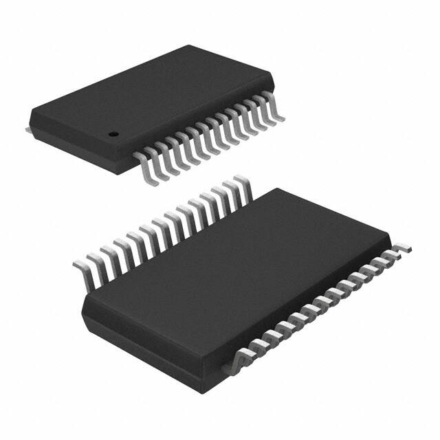
30-Pin SSOP (DB) and 32-Pin TSSOP (DAP)
Compatible With 3.3-V, 5-V and 12-V PC Cards
Low rDS(on) (140-mΩ 5-V VCC Switch; 110-mΩ
3.3-V VCC Switch)
Break-Before-Make Switching
DB OR DF PACKAGE
(TOP VIEW)
5V
5V
DATA
CLOCK
LATCH
RESET
12V
AVPP
AVCC
AVCC
AVCC
GND
NC
RESET
3.3V
1
2
3
4
5
6
7
8
9
10
11
12
13
14
15
30
29
28
27
26
25
24
23
22
21
20
19
18
17
16
5V
NC
NC
NC
NC
NC
12V
BVPP
BVCC
BVCC
BVCC
NC
OC
3.3V
3.3V
DAP PACKAGE
(TOP VIEW)
description
The TPS2206 PC Card power-interface switch
provides an integrated power-management solution
for two PC Cards. All of the discrete power
MOSFETs, a logic section, current limiting, and
thermal protection for PC Card control are
combined on a single integrated circuit (IC), using
the Texas Instruments LinBiCMOS process.
The circuit allows the distribution of 3.3-V, 5-V,
and/or 12-V card power by means of the P2C
(PCMCIA Peripheral-Control) Texas Instruments
nonproprietary serial interface. The current-limiting
feature eliminates the need for fuses, which
reduces component count and improves reliability.
The TPS2206 is backward compatible with the
TPS2202 and TPS2202A, except that there is no
VDD connection. Bias current is derived from
either the 3.3-V input pin or the 5-V input pin. The
TPS2206 also eliminates the APWR_GOOD and
BPWR_GOOD pins of the TPS2202 and
TPS2202A.
5V
5V
NC
DATA
CLOCK
LATCH
RESET
12V
AVPP
AVCC
AVCC
AVCC
GND
RESET
NC
3.3V
1
2
3
4
5
6
7
8
9
10
11
12
13
14
15
16
32
31
30
29
28
27
26
25
24
23
22
21
20
19
18
17
5V
NC
NC
NC
NC
NC
NC
12V
BVPP
BVCC
BVCC
BVCC
OC
NC
3.3V
3.3V
NC − No internal connection
The TPS2206 features a 3.3-V low-voltage mode that allows for 3.3-V switching without the need for 5 V. This
facilitates low-power system designs such as sleep mode and pager mode where only 3.3 V is available.
Please be aware that an important notice concerning availability, standard warranty, and use in critical applications of
Texas Instruments semiconductor products and disclaimers thereto appears at the end of this data sheet.
LinBiCMOS and P2C are trademarks of Texas Instruments.
PC Card and CardBus are trademarks of PCMCIA (Personal Computer Memory Card International Association).
Copyright 2001, Texas Instruments Incorporated
�����
���� � � ����������� �� �!��"�� �� �� #!$%������� &��"'
���&!��� ������� �� �#"����������� #"� �(" �"��� �� �")�� �����!�"���
����&��& *������+' ���&!����� #���"����, &�"� ��� �"�"�����%+ ���%!&"
�"����, �� �%% #����"�"��'
POST OFFICE BOX 655303
• DALLAS, TEXAS 75265
1
��������
��
��
�� �
�� ������������
� ����
�
���� ����� ��� ����
�
�
�
�����
��
SLVS138D − MAY 1996 − REVISED JANUARY 2001
description (continued)
The TPS2206 incorporates a reset function, selectable by one of two inputs, to help alleviate system errors. The
reset function enables PC Card initialization concurrent with host platform initialization, allowing a system reset.
Reset is accomplished by grounding the VCC and Vpp (flash-memory programming voltage) outputs, which
discharges residual card voltage.
End equipment for the TPS2206 includes notebook computers, desktop computers, personal digital assistants
(PDAs), digital cameras and bar-code scanners.
AVAILABLE OPTIONS
PACKAGED DEVICES
TA
PLASTIC SMALL OUTLINE (DB)
PLASTIC SMALL OUTLINE (DF)
TSSOP (DAP)
−40°C to 85°C
TPS2206IDB
TPS2206IDFR
TPS2206IDAPR
CHIP FORM (Y)
TPS2206Y
The DB package is available taped and reeled (add an R suffix to the device type, e.g., TPS2206IDBR). The DF and DAP packages are only
available taped and reeled, indicated by the R suffix.
typical PC card power-distribution application
Power Supply
12V
5V
3.3V
12 V
5V
3.3 V
RESET
RESET
Supervisor
3
PCMCIA
Controller
Serial Interface
OC
2
TPS2206
AVPP
AVCC
AVCC
Vpp1
Vpp2
VCC
VCC
PC
Card A
Vpp1
Vpp2
VCC
VCC
PC
Card B
AVCC
BVPP
BVCC
BVCC
BVCC
POST OFFICE BOX 655303
• DALLAS, TEXAS 75265
��������
��
��
�� �
�� ������������
� ����
�
���� ����� ��� ����
�
�
�
�����
��
SLVS138D − MAY 1996 − REVISED JANUARY 2001
TPS2206Y chip information
This chip, when properly assembled, displays characteristics similar to those of the TPS2206. Thermal
compression or ultrasonic bonding may be used on the doped-aluminum bonding pads. The chips may be
mounted with conductive epoxy or a gold-silicon preform.
BONDING PAD ASSIGNMENTS
4
3
2
5
1
23
6
7
22
8
21
144
9
20
10
19
5V
1
5V
2
23
5V
DATA
3
22
12V
CLOCK
4
21
BVPP
LATCH
5
20
BVCC
RESET
6
19
BVCC
12V
7
18
BVCC
AVPP
8
17
OC
AVCC
9
16
3.3V
AVCC
10
15
3.3V
AVCC
11
14
3.3V
GND
12
13
RESET
TPS2206Y
CHIP THICKNESS: 15 TYPICAL
11
12
18
13
15
14
16
17
BONDING PADS: 4 × 4 MINIMUM
TJ max = 150°C
TOLERANCES ARE ± 10%.
ALL DIMENSIONS ARE IN MILS.
142
POST OFFICE BOX 655303
• DALLAS, TEXAS 75265
3
��������
��
��
�� �
�� ������������
� ����
�
���� ����� ��� ����
�
�
�
�����
��
SLVS138D − MAY 1996 − REVISED JANUARY 2001
Terminal Functions
TERMINAL
NAME
3.3V
NO.
I/O
DB, DF
DAP
DESCRIPTION
15, 16, 17
16, 17, 18
I
3.3-V VCC input for card power
5V
1, 2, 30
1, 2, 32
I
5-V VCC input for card power and/or chip power
12V
7, 24
8, 25
I
12-V Vpp input for card power
AVCC
9, 10, 11
10, 11, 12
O
Switched output that delivers 0 V, 3.3 V, 5 V, or high impedance to card
AVPP
8
9
O
Switched output that delivers 0 V, 3.3 V, 5 V, 12 V, or high impedance to card
BVCC
20, 21, 22
21, 22, 23
O
Switched output that delivers 0 V, 3.3 V, 5 V, or high impedance
BVPP
23
24
O
Switched output that delivers 0 V, 3.3 V, 5 V, 12 V, or high impedance
4
5
I
Logic-level clock for serial data word
I
Logic-level serial data word
CLOCK
DATA
3
4
GND
12
13
5
6
NC
13, 19, 25,
26, 27,
28, 29
3, 19, 26,
27, 28, 29,
30, 31
OC
18
20
O
Logic-level overcurrent. OC reports output that goes low when an overcurrent condition exists
LATCH
Ground
I
Logic-level latch for serial data word
No internal connection
RESET
6
7
I
Logic-level RESET input active high. Do not connect if terminal 14 is used.
RESET
14
14
I
Logic-level RESET input active low. Do not connect if terminal 6 is used.
absolute maximum ratings over operating free-air temperature (unless otherwise noted)†
Input voltage range for card power: VI(5V) . . . . . . . . . . . . . . . . . . . . . . . . . . . . . . . . . . . . . . . . . . . . −0.3 V to 7 V
VI(3.3V) . . . . . . . . . . . . . . . . . . . . . . . . . . . . . . . . . . . . . . . . . . . −0.3 V to 7 V
VI(12V) . . . . . . . . . . . . . . . . . . . . . . . . . . . . . . . . . . . . . . . . . . −0.3 V to 14 V
Logic input voltage . . . . . . . . . . . . . . . . . . . . . . . . . . . . . . . . . . . . . . . . . . . . . . . . . . . . . . . . . . . . . . . . . −0.3 V to 7 V
Continuous total power dissipation . . . . . . . . . . . . . . . . . . . . . . . . . . . . . . . . . . . . . See Dissipation Rating Table
Output current (each card): IO(xVCC) . . . . . . . . . . . . . . . . . . . . . . . . . . . . . . . . . . . . . . . . . . . . . . . internally limited
IO(xVPP) . . . . . . . . . . . . . . . . . . . . . . . . . . . . . . . . . . . . . . . . . . . . . . . internally limited
Operating virtual junction temperature range, TJ . . . . . . . . . . . . . . . . . . . . . . . . . . . . . . . . . . . . . −40°C to 150°C
Operating free-air temperature range, TA . . . . . . . . . . . . . . . . . . . . . . . . . . . . . . . . . . . . . . . . . . . . −40°C to 85°C
Storage temperature range, Tstg . . . . . . . . . . . . . . . . . . . . . . . . . . . . . . . . . . . . . . . . . . . . . . . . . . . −55°C to 150°C
Lead temperature 1,6 mm (1/16 inch) from case for 10 seconds . . . . . . . . . . . . . . . . . . . . . . . . . . . . . . . 260°C
† Stresses beyond those listed under “absolute maximum ratings” may cause permanent damage to the device. These are stress ratings only, and
functional operation of the device at these or any other conditions beyond those indicated under “recommended operating conditions” is not
implied. Exposure to absolute-maximum-rated conditions for extended periods may affect device reliability.
DISSIPATION RATING TABLE
PACKAGE
TA ≤ 25°C
POWER RATING
DERATING FACTOR‡
ABOVE TA = 25°C
TA = 70°C
POWER RATING
TA = 85°C
POWER RATING
DB
1024 mW
8.2 mW/°C
655 mW
532 mW
DF
1158 mW
9.26 mW/°C
741 mW
602 mW
1625 mW
13 mW/°C
1040 mW
845 mW
No backplane
DAP
Backplane§
6044 mW
48.36 mW/°C
3869 mW
3143 mW
‡ These devices are mounted on an FR4 board with no special thermal considerations.
§ 2-oz backplane with 2-oz traces; 5.2-mm × 11-mm thermal pad with 6-mil solder; 0.18-mm diameter vias in a 3×6 array.
4
POST OFFICE BOX 655303
• DALLAS, TEXAS 75265
��������
��
��
�� �
�� ������������
� ����
�
���� ����� ��� ����
�
�
�
�����
��
SLVS138D − MAY 1996 − REVISED JANUARY 2001
recommended operating conditions
Input voltage range, VI
Output current
MIN
MAX
UNIT
VI(5V)
VI(3.3V)
0
5.25
V
0
5.25
V
VI(12V)
IO(xVCC) at 25°C
0
13.5
V
1
IO(xVPP) at 25°C
Clock frequency
Operating virtual junction temperature, TJ
A
150
mA
0
2.5
MHz
−40
125
°C
electrical characteristics, TA = 25°C, VI(5V) = 5 V (unless otherwise noted)
dc characteristics
TPS2206
PARAMETER
TEST CONDITIONS
MIN
5 V to xVCC
3.3 V to xVCC
Switch resistances†
VO(xVPP)
VO(xVCC)
Ilkg
II
IOS
3.3 V to xVCC
103
140
69
110
96
180
6
3.3 V to xVPP
6
12 V to xVPP
1
Ipp at 10 mA
ICC at 10 mA
Clamp low voltage
UNIT
mΩ
Ω
0.8
V
0.8
V
1
Ipp high-impedance state
TA = 25°C
TA = 85°C
1
ICC high-impedance state
TA = 25°C
TA = 85°C
VI(5V) = 5 V
VO(AVCC) = VO(BVCC) = 5 V,
VO(AVPP) = VO(BVPP) = 12 V
117
150
VI(5V) = 0,
VI(3.3V) = 3.3 V
VO(AVCC) = VO(BVCC) = 3.3 V,
VO(AVPP) = VO(BVPP) = 0
131
150
Shutdown mode
VO(BVCC) = VO(AVCC) = VO(AVPP)
= VO(BVPP) = Hi-Z
IO(xVCC)
IO(xVPP)
TJ = 85
85°C,
C,
Output powered up into a short to GND
Leakage current
Short-circuit
output-current limit
VI(3.3 V) = 3.3 V
VI(3.3V) = 3.3 V
MAX
5 V to xVPP
Clamp low voltage
Input current
VI(5V) = 5 V,
VI(5V) = 0,
TYP
10
50
10
A
µA
50
A
µA
1
µA
1
2.2
A
120
400
mA
† Pulse-testing techniques are used to maintain junction temperature close to ambient temperature; thermal effects must be taken into account
separately.
logic section
TPS2206
PARAMETER
TEST CONDITIONS
MIN
Logic input current
MAX
1
Logic input high level
2
Logic input low level
VI(5V)= 5 V,
IO = 1mA
VI(5V)= 0,
VI(3.3V) = 3.3 V
IO = 1mA,
Logic output low level
IO = 1mA
POST OFFICE BOX 655303
• DALLAS, TEXAS 75265
µA
V
0.8
Logic output high level
UNIT
V
VI(5V)−0.4
V
VI(3.3V)−0.4
0.4
V
5
��������
��
��
�� �
�� ������������
� ����
�
���� ����� ��� ����
�
�
�
�����
��
SLVS138D − MAY 1996 − REVISED JANUARY 2001
switching characteristics†‡
TPS2206
PARAMETER
tr
tf
tpd
TEST CONDITIONS
MIN
TYP
VO(xVCC)
VO(xVPP)
1.2
Output rise time
10
Output fall time
VO(xVCC)
VO(xVPP)
MAX
UNIT
5
ms
14
4.4
ms
LATCH↑ to VO(xVPP)
ton
toff
18
ms
ton
toff
6.5
ms
LATCH↑ to VO(xVCC) (3.3 V), VI(5V) = 5 V
20
ms
ton
toff
5.7
ms
LATCH↑ to VO(xVCC) (5 V)
25
ms
ton
toff
6.6
ms
LATCH↑ to VO(xVCC) (3.3 V), VI(5V) = 0
21
ms
Propagation delay (see Figure 1)
† Refer to Parameter Measurement Information
‡ Switching Characteristics are with CL = 150 µF.
electrical characteristics, TA = 25°C, VI(5V) = 5 V (unless otherwise noted)
dc characteristics
TPS2206Y
PARAMETER
TEST CONDITIONS
5 V to xVCC
3.3 V to xVCC
Switch resistances§
VO(xVPP)
VO(xVCC)
Ilkg
3.3 V to xVCC
69
4.74
Ipp at 10 mA
ICC at 10 mA
VI(5V) = 0,
VI(3.3V) = 3.3 V
UNIT
mΩ
4.74
0.724
Ipp High-impedance state
ICC High-impedance state
MAX
96
12 V to xVPP
Clamp low voltage
Input current
VI(3.3 V) = 3.3 V
VI(3.3V) = 3.3 V
3.3 V to xVPP
VI(5V) = 5 V
II
TYP
103
VI(5V) = 5 V,
VI(5V) = 0,
5 V to xVPP
Clamp low voltage
Leakage current
MIN
TA = 25°C
TA = 25°C
VO(AVCC) = VO(BVCC) = 5 V,
VO(AVPP) = VO(BVPP) = 12 V
VO(AVCC) = VO(BVCC) = 3.3 V,
VO(AVPP) = VO(BVPP) = 0
Ω
0.275
V
0.275
V
1
1
A
µA
117
µA
131
§ Pulse-testing techniques are used to maintain junction temperature close to ambient temperature; thermal effects must be taken into account
separately.
6
POST OFFICE BOX 655303
• DALLAS, TEXAS 75265
��������
��
��
�� �
�� ������������
� ����
�
���� ����� ��� ����
�
�
�
�����
��
SLVS138D − MAY 1996 − REVISED JANUARY 2001
switching characteristics†‡
TPS2206Y
PARAMETER
tr
tf
tpd
TEST CONDITIONS
MIN
TYP
VO(xVCC)
VO(xVPP)
1.2
Output rise time
10
Output fall time
VO(xVCC)
VO(xVPP)
MAX
UNIT
5
ms
14
4.4
ms
LATCH↑ to VO(xVPP)
ton
toff
18
ms
6.5
ms
LATCH↑ to VO(xVCC) (3.3 V), VI(5V) = 5 V
ton
toff
20
ms
ton
toff
5.7
ms
LATCH↑ to VO(xVCC) (5 V)
25
ms
ton
toff
6.6
ms
LATCH↑ to VO(xVCC) (3.3 V), VI(5V) = 0
21
ms
Propagation delay (see Figure 1)
† Refer to Parameter Measurement Information
‡ Switching Characteristics are with CL = 150 µF.
PARAMETER MEASUREMENT INFORMATION
Vpp
VCC
CL
CL
LOAD CIRCUIT
LOAD CIRCUIT
VDD
LATCH
50%
VDD
50%
LATCH
GND
GND
toff
toff
ton
ton
VI(12V)
90%
VO(xVPP)
10%
10%
GND
VOLTAGE WAVEFORMS
VI(5V)
90%
VO(xVCC)
GND
VOLTAGE WAVEFORMS
Figure 1. Test Circuits and Voltage Waveforms
POST OFFICE BOX 655303
• DALLAS, TEXAS 75265
7
��������
��
��
�� �
�� ������������
� ����
�
���� ����� ��� ����
�
�
�
�����
��
SLVS138D − MAY 1996 − REVISED JANUARY 2001
PARAMETER MEASUREMENT INFORMATION
Table of Timing Diagrams
FIGURE
Serial-Interface Timing
2
xVCC Propagation Delay and Rise Time With 1-µF Load, 3.3-V Switch, VI(5V) = 5 V
3
xVCC Propagation Delay and Fall Time With 1-µF Load, 3.3-V Switch, VI(5V) = 5 V
4
xVCC Propagation Delay and Rise Time With 150-µF Load, 3.3-V Switch, VI(5V) = 5 V
5
xVCC Propagation Delay and Fall Time With 150-µF Load, 3.3-V Switch, VI(5V) = 5 V
6
xVCC Propagation Delay and Rise Time With 1-µF Load, 3.3-V Switch, VI(5V) = 0
7
xVCC Propagation Delay and Fall Time With 1-µF Load, 3.3-V Switch, VI(5V) = 0
8
xVCC Propagation Delay and Rise Time With 150-µF Load, 3.3-V Switch, VI(5V) = 0
9
xVCC Propagation Delay and Fall Time With 150-µF Load, 3.3-V Switch, VI(5V) = 0
10
xVCC Propagation Delay and Rise Time With 1-µF Load, 5-V Switch
11
xVCC Propagation Delay and Fall Time With 1-µF Load, 5-V Switch
12
xVCC Propagation Delay and Rise Time With 150-µF Load, 5-V Switch
13
xVCC Propagation Delay and Fall Time With 150-µF Load, 5-V Switch
14
xVPP Propagation Delay and Rise Time With 1-µF Load, 12-V Switch
15
xVPP Propagation Delay and Fall Time With 1-µF Load, 12-V Switch
16
xVPP Propagation Delay and Rise Time With 150-µF Load, 12-V Switch
17
xVPP Propagation Delay and Fall Time With 150-µF Load, 12-V Switch
18
DATA
D8
D7
D6
D5
D4
D3
D2
D1
D0
LATCH
CLOCK
NOTE A: Data is clocked in on the positive leading edge of the clock. The latch should occur before the next positive leading edge of
the clock. For definition of D0 to D8, see the control logic table.
Figure 2. Serial-Interface Timing
8
POST OFFICE BOX 655303
• DALLAS, TEXAS 75265
��������
��
��
�� �
�� ������������
� ����
�
���� ����� ��� ����
�
�
�
�����
��
SLVS138D − MAY 1996 − REVISED JANUARY 2001
PARAMETER MEASUREMENT INFORMATION
LATCH (2 V/div)
LATCH (2 V/div)
xVCC (2 V/div)
0
1
2
3
xVCC (2 V/div)
4
5
6
7
8
9
0
5
10
15
20
25
30
35
40
t − Time − ms
t − Time − ms
Figure 3. xVCC Propagation Delay and
Rise Time With 1-µF Load, 3.3-V Switch,
(VI(5V) = 5 V)
Figure 4. xVCC Propagation Delay and
Fall Time With 1-µF Load, 3.3-V Switch,
(VI(5V) = 5 V)
LATCH (2 V/div)
LATCH (2 V/div)
xVCC (2 V/div)
xVCC (2 V/div)
0
1
2
3
45
4
5
6
7
8
9
0
5
t − Time − ms
10
15
20
25
30
35
40
45
t − Time − ms
Figure 5. xVCC Propagation Delay and
Rise Time With 150-µF Load, 3.3-V Switch,
VI(5V) = 5 V
POST OFFICE BOX 655303
Figure 6. xVCC Propagation Delay and
Fall Time With 150-µF Load, 3.3-V Switch,
VI(5V) = 5 V
• DALLAS, TEXAS 75265
9
��������
��
��
�� �
�� ������������
� ����
�
���� ����� ��� ����
�
�
�
�����
��
SLVS138D − MAY 1996 − REVISED JANUARY 2001
PARAMETER MEASUREMENT INFORMATION
LATCH (2 V/div)
LATCH (2 V/div)
xVCC (2 V/div)
0
1
2
3
xVCC (2 V/div)
4
5
6
7
8
9
0
5
10
15
20
25
35
40
t − Time − ms
Figure 7. xVCC Propagation Delay and
Rise Time With 1-µF Load, 3.3-V Switch,
VI(5V) = 0
Figure 8. xVCC Propagation Delay and
Fall Time With 1-µF Load, 3.3-V Switch,
VI(5V) = 0
xVCC (2 V/div)
xVCC (2 V/div)
0
1
2
3
45
LATCH (2 V/div)
LATCH (2 V/div)
4
5
6
7
8
9
0
5
10
15
20
25
30
35
40
45
t − Time − ms
t − Time − ms
Figure 9. xVCC Propagation Delay and
Rise Time With 150-µF Load, 3.3-V Switch,
VI(5V) = 0
10
30
t − Time − ms
POST OFFICE BOX 655303
Figure 10. xVCC Propagation Delay and
Fall Time With 150-µF Load, 3.3-V Switch,
VI(5V) = 0
• DALLAS, TEXAS 75265
��������
��
��
�� �
�� ������������
� ����
�
���� ����� ��� ����
�
�
�
�����
��
SLVS138D − MAY 1996 − REVISED JANUARY 2001
PARAMETER MEASUREMENT INFORMATION
LATCH (2 V/div)
LATCH (2 V/div)
xVCC (2 V/div)
xVCC (2 V/div)
0
1
2
3
4
0
5
10
t − Time − ms
15
20
25
30
35
40
45
t − Time − ms
Figure 11. xVCC Propagation Delay and
Rise Time With 1-µF Load, 5-V Switch
Figure 12. xVCC Propagation Delay and
Fall Time With 1-µF Load, 5-V Switch
LATCH (2 V/div)
LATCH (2 V/div)
xVCC (2 V/div)
xVCC (2 V/div)
0
1
2
3
4
5
6
7
8
9
0
5
t − Time − ms
10
15
20
25
30
35
40
45
t − Time − ms
Figure 13. xVCC Propagation Delay and
Rise Time With 150-µF Load, 5-V Switch
POST OFFICE BOX 655303
Figure 14. xVCC Propagation Delay and
Fall Time With 150-µF Load, 5-V Switch
• DALLAS, TEXAS 75265
11
��������
��
��
�� �
�� ������������
� ����
�
���� ����� ��� ����
�
�
�
�����
��
SLVS138D − MAY 1996 − REVISED JANUARY 2001
PARAMETER MEASUREMENT INFORMATION
LATCH (2 V/div)
LATCH (2 V/div)
xVPP (5 V/div)
xVPP (5 V/div)
0
0.2
0.4 0.6
0.8
1.0
1.2
1.4
1.6
1.8
0
1
2
3
4
5
6
7
8
9
t − Time − ms
t − Time − ms
Figure 16. xVPP Propagation Delay and
Fall Time With 1-µF Load, 12-V Switch
Figure 15. xVPP Propagation Delay and
Rise Time With 1-µF Load, 12-V Switch
LATCH (2 V/div)
LATCH (2 V/div)
xVPP (5 V/div)
xVPP (5 V/div)
0
1
2
3
4
5
6
7
8
9
0
t − Time − ms
10
15
20
25
30
35
40
45
t − Time − ms
Figure 17. xVPP Propagation Delay and
Rise Time With 150-µF Load, 12-V Switch
12
5
POST OFFICE BOX 655303
Figure 18. xVPP Propagation Delay and
Fall Time With 150-µF Load, 12-V Switch
• DALLAS, TEXAS 75265
��������
��
��
�� �
�� ������������
� ����
�
���� ����� ��� ����
�
�
�
�����
��
SLVS138D − MAY 1996 − REVISED JANUARY 2001
TYPICAL CHARACTERISTICS
Table of Graphs
FIGURE
IDD
IDD
Supply current, VI(5V) = 5 V
vs Junction temperature
19
Supply current, VI(5V) = 0
vs Junction temperature
20
rDS(on)
Static drain-source on-state resistance, 3.3-V switch, VI(5V) = 5 V
vs Junction temperature
21
rDS(on)
Static drain-source on-state resistance, 3.3-V switch, VI(5V) = 0
vs Junction temperature
22
rDS(on)
Static drain-source on-state resistance, 5-V switch
vs Junction temperature
23
rDS(on)
Static drain-source on-state resistance, 12-V switch
vs Junction temperature
24
VO(xVCC)
VO(xVCC)
Output voltage, 5-V switch
vs Output current
25
Output voltage, 3.3-V switch, VI(5V) = 5 V
vs Output current
26
VO(xVCC)
VO(xVPP)
Output voltage, 3.3-V switch, VI(5V) = 0
vs Output current
27
Output voltage, 12-V switch
vs Output current
28
IOS(xVCC)
IOS(xVCC)
Short-circuit current, 5-V switch
vs Junction temperature
29
Short-circuit current, 3.3-V switch
vs Junction temperature
30
IOS(xVPP)
Short-circuit current, 12-V switch
vs Junction temperature
31
SUPPLY CURRENT
vs
JUNCTION TEMPERATURE
SUPPLY CURRENT
vs
JUNCTION TEMPERATURE
155
150
145
I CC − Supply Current − µ A
I CC − Supply Current − µ A
150
155
VO(AVCC) = VO(BVCC) = 5 V
VO(AVPP) = VO(BVPP) = 12 V
No load
140
135
130
ÁÁ
ÁÁ
140
135
130
ÁÁ
ÁÁ
125
120
125
120
115
115
110
−50
145
VO(AVCC) = VO(BVCC) = 3.3 V
VO(AVPP) = VO(BVPP) = 0 V
VI(5V) = 0
No load
−25
0
25
50
75
100
125
110
−50
−25
0
25
50
75
100
125
TJ − Junction Temperature − °C
TJ − Junction Temperature − °C
Figure 20
Figure 19
POST OFFICE BOX 655303
• DALLAS, TEXAS 75265
13
��������
��
��
�� �
�� ������������
� ����
�
���� ����� ��� ����
�
�
�
�����
��
SLVS138D − MAY 1996 − REVISED JANUARY 2001
3.3-V SWITCH
3.3-V SWITCH
STATIC DRAIN-SOURCE ON-STATE RESISTANCE
vs
JUNCTION TEMPERATURE
STATIC DRAIN-SOURCE ON-STATE RESISTANCE
vs
JUNCTION TEMPERATURE
220
200
VI(5V) = 5 V
VI(3.3V) = 3.3 V
VCC = 3.3 V
180
160
140
120
100
80
60
−50
−25
0
25
50
75
100
125
r DS(on) − Static Drain-Source On-State Resistance − m Ω
r DS(on) − Static Drain-Source On-State Resistance − m Ω
TYPICAL CHARACTERISTICS
220
200
VI(5V) = 0
VI(3.3V) = 3.3 V
VCC = 3.3 V
180
160
140
120
100
80
60
−50
−25
TJ − Junction Temperature − °C
25
50
75
100
125
Figure 22
5-V SWITCH
12-V SWITCH
STATIC DRAIN-SOURCE ON-STATE RESISTANCE
vs
JUNCTION TEMPERATURE
STATIC DRAIN-SOURCE ON-STATE RESISTANCE
vs
JUNCTION TEMPERATURE
240
220
VI(5V) = 5 V
VCC = 5 V
200
180
160
140
120
100
80
60
−50
−25
0
25
50
75
100
125
r DS(on) − Static Drain-Source On-State Resistance − m Ω
r DS(on) − Static Drain-Source On-State Resistance − m Ω
Figure 21
1100
1000
VI(5V) = 5 V
Vpp = 12 V
900
800
700
600
500
−50
−25
0
25
Figure 24
Figure 23
POST OFFICE BOX 655303
50
75
100
TJ − Junction Temperature − °C
TJ − Junction Temperature − °C
14
0
TJ − Junction Temperature − °C
• DALLAS, TEXAS 75265
125
��������
��
��
�� �
�� ������������
� ����
�
���� ����� ��� ����
�
�
�
�����
��
SLVS138D − MAY 1996 − REVISED JANUARY 2001
TYPICAL CHARACTERISTICS
5-V SWITCH
3.3-V SWITCH
OUTPUT VOLTAGE
vs
OUTPUT CURRENT
OUTPUT VOLTAGE
vs
OUTPUT CURRENT
3.3
5
25°C
−40°C
4.95
VO(xVCC) − Output Voltage − V
VO(xVCC) − Output Voltage − V
3.27
−40°C
85°C
4.9
125°C
4.85
VI(5V) = 5 V
VCC = 5 V
4.8
85°C
3.24
125°C
3.21
3.18
3.15
0
0.2
0.4
0.6
0.8
IO(xVCC) − Output Current − A
25°C
1
VI(5V) = 5 V
VI(3.3V) = 3.3 V
VCC = 3.3 V
0
Figure 25
0.2
0.4
0.6
0.8
IO(xVCC) − Output Current − A
Figure 26
3.3-V SWITCH
12-V SWITCH
OUTPUT VOLTAGE
vs
OUTPUT CURRENT
OUTPUT VOLTAGE
vs
OUTPUT CURRENT
12
3.3
−40°C
−40°C
25°C
11.98
25°C
3.25
VO(xVPP) − Output Voltage − V
VO(xVCC) − Output Voltage − V
1
85°C
3.2
125°C
3.15
11.96
85°C
125°C
11.94
11.92
VI(5 V) = 5 V
VPP = 12 V
VI(5 V) = 0 V
VCC = 3.3 V
11.9
3.1
0
0.2
0.8
0.6
IO(xVCC) − Output Current − A
0.4
1
0
Figure 27
0.03
0.06
0.09
IO(xVPP) − Output Current − A
0.12
Figure 28
POST OFFICE BOX 655303
• DALLAS, TEXAS 75265
15
��������
��
��
�� �
�� ������������
� ����
�
���� ����� ��� ����
�
�
�
�����
��
SLVS138D − MAY 1996 − REVISED JANUARY 2001
TYPICAL CHARACTERISTICS
5-V SWITCH
3.3-V SWITCH
SHORT-CIRCUIT CURRENT
vs
JUNCTION TEMPERATURE
SHORT-CIRCUIT CURRENT
vs
JUNCTION TEMPERATURE
2
VI(5V) = 5 V
VCC = 5 V
I OS(xVCC) − Short-Circuit Current − A
I OS(xVCC) − Short-Circuit Current − A
2
1.8
1.6
1.4
1.2
1
0.8
−50
0
25
75
−25
50
100
TJ − Junction Temperature − °C
1.8
VI(5V) = 0
VI(3.3V) = 3.3 V
VCC = 3.3 V
1.6
1.4
1.2
1
0.8
−50
125
−25
50
100
0
25
75
TJ − Junction Temperature − °C
Figure 29
Figure 30
12-V SWITCH
SHORT-CIRCUIT CURRENT
vs
JUNCTION TEMPERATURE
I OS(xVPP) − Short-Circuit Current − A
0.32
VI(5V) = 5 V
Vpp = 12 V
0.3
0.28
0.26
0.24
0.22
0.2
−50
−25
50
100
0
25
75
TJ − Junction Temperature − °C
Figure 31
16
POST OFFICE BOX 655303
• DALLAS, TEXAS 75265
125
125
��������
��
��
�� �
�� ������������
� ����
�
���� ����� ��� ����
�
�
�
�����
��
SLVS138D − MAY 1996 − REVISED JANUARY 2001
APPLICATION INFORMATION
overview
PC Cards were initially introduced as a means to add EEPROM (flash memory) to portable computers with
limited on-board memory. The idea of add-in cards quickly took hold; modems, wireless LANs, Global
Positioning Satellite System (GPS), multimedia, and hard-disk versions were soon available. As the number
of PC Card applications grew, the engineering community quickly recognized the need for a standard to ensure
compatibility across platforms. To this end, the PCMCIA was established, comprised of members from leading
computer, software, PC Card, and semiconductor manufacturers. One key goal was to realize the plug-and-play
concept. Cards and hosts from different vendors should be compatible—able to communicate with one another
transparently.
PC Card power specification
System compatibility also means power compatibility. The most current set of specifications (PC Card Standard)
set forth by the PCMCIA committee states that power is to be transferred between the host and the card through
eight of the 68 terminals of the PC Card connector. This power interface consists of two VCC, two Vpp, and four
ground terminals. Multiple VCC and ground terminals minimize connector-terminal and line resistance. The two
Vpp terminals were originally specified as separate signals but are commonly tied together in the host to form
a single node to minimize voltage losses. Card primary power is supplied through the VCC terminals;
flash-memory programming and erase voltage is supplied through the Vpp terminals.
designing for voltage regulation
The current PCMCIA specification for output-voltage regulation (VO(reg)) of the 5-V output is 5% (250 mV). In
a typical PC power-system design, the power supply has an output-voltage regulation (VPS(reg)) of 2% (100 mV).
Also, a voltage drop from the power supply to the PC Card will result from resistive losses (VPCB) in the PCB
traces and the PCMCIA connector. A typical design would limit the total of these resistive losses to less than
1% (50 mV) of the output voltage. Therefore, the allowable voltage drop (VDS) for the TPS2206 would be the
PCMCIA voltage regulation less the power supply regulation and less the PCB and connector resistive drops:
V
DS
+V
OǒregǓ
–V
PSǒregǓ
–V
(1)
PCB
Typically, this would leave 100 mV for the allowable voltage drop across the TPS2206. The voltage drop is the
output current multiplied by the switch resistance of the TPS2206. Therefore, the maximum output current that
can be delivered to the PC Card in regulation is the allowable voltage drop across the TPS2206 divided by the
output switch resistance.
V
I max + r DS
O
DSǒonǓ
(2)
The xVCC outputs have been designed to deliver 700 mA at 5 V within regulation over the operating temperature
range. Current proposals for the PCMCIA specifications are to limit the power dissipated in the PCMCIA slot
to 3 W. With an input voltage of 5 V, 700 mA continuous is the maximum current that can be delivered to the
PC Card. The TPS2206 is capable of delivering up to 1 A continuously, but during worst-case conditions the
output may not be within regulation. This is generally acceptable because the majority of PC Cards require less
than 700 mA continuous. Some cards require higher peak currents (disk drives during initial platter spin-up),
but it is generally acceptable for small voltage sags to occur during these peak currents.
The xVCC outputs have been designed to deliver 1 A continuously at 3.3 V within regulation over the operating
temperature range. The PCMCIA specification for output voltage regulation of the 3.3-V output is 300 mV. Using
the voltage drop percentages (2%) for power supply regulation and PCB resistive loss (1%), the allowable
voltage drop for the 3.3 V switch is 200 mV.
The xVPP outputs have been designed to deliver 150 mA continuously at 12 V.
POST OFFICE BOX 655303
• DALLAS, TEXAS 75265
17
��������
��
��
�� �
�� ������������
� ����
�
���� ����� ��� ����
�
�
�
�����
��
SLVS138D − MAY 1996 − REVISED JANUARY 2001
APPLICATION INFORMATION
overcurrent and overtemperature protection
PC Cards are inherently subject to damage that can result from mishandling. Host systems require protection
against short-circuited cards that could lead to power supply or PCB-trace damage. Even systems robust
enough to withstand a short circuit would still undergo rapid battery discharge into the damaged PC Card,
resulting in the rather sudden and unacceptable loss of system power. Most hosts include fuses for protection.
However, the reliability of fused systems is poor, as blown fuses require troubleshooting and repair, usually by
the manufacturer.
The TPS2206 takes a two-pronged approach to overcurrent protection. First, instead of fuses, sense FETs
monitor each of the power outputs. Excessive current generates an error signal that linearly limits the output
current, preventing host damage or failure. Sense FETs, unlike sense resistors or polyfuses, have an added
advantage in that they do not add to the series resistance of the switch and thus produce no additional voltage
losses. Second, when an overcurrent condition is detected, the TPS2206 asserts a signal at OC that can be
monitored by the microprocessor to initiate diagnostics and/or send the user a warning message. In the event
that an overcurrent condition persists, causing the IC to exceed its maximum junction temperature,
thermal-protection circuitry activates, shutting down all power outputs until the device cools to within a safe
operating region.
12-V supply not required
Most PC Card switches use the externally supplied 12-V Vpp power for switch-gate drive and other chip functions,
which requires that power be present at all times. The TPS2206 offers considerable power savings by using
an internal charge pump to generate the required higher voltages from the 5-V or 3.3-V input; therefore, the
external 12-V supply can be disabled except when needed for flash-memory functions, thereby extending
battery lifetime. Do not ground the 12-V input if the 12-V input is not used. Additional power savings are realized
by the TPS2206 during a software shutdown in which quiescent current drops to a maximum of 1 µA.
backward compatibility and 3.3-V low-voltage mode
The TPS2206 is backward compatible with the TPS2202 AND TPS2202A products, with the following
considerations. Pin 25 (VDD on TPS2202/TPS2202A) is a no connect because bias current is derived from
either the 3.3-V input pin or the 5-V input pin. Also, the TPS2206 does not have the APWR_GOOD or
BPWR_GOOD VPP reporting outputs. These are left as no connects.
The TPS2206 operates in 3.3-V low-voltage mode when 3.3 volts is the only available input voltage (VI(5V)=0).
This allows host and PC Cards to be operated in low-power 3.3-V-only modes such as sleep modes or pager
modes. Note that in this operation mode, the TPS2206 derives its bias current from the 3.3-V input pin and only
3.3 V can be delivered to the PC Card. The 3.3-V switch resistance increases, but the added switch resistance
should not be critical, because only a small amount of current is delivered in this mode. If 6% (198 mV) is allowed
for the 3.3-V switch voltage drop, a 500-mΩ switch could deliver over 350 mA to the PC Card.
voltage transitioning requirement
PC Cards, like portables, are migrating from 5 V to 3.3 V to minimize power consumption, optimize board space,
and increase logic speeds. The TPS2206 is designed to meet all combinations of power delivery as currently
defined in the PCMCIA standard. The latest protocol accommodates mixed 3.3-V/5-V systems by first powering
the card with 5 V, then polling it to determine its 3.3-V compatibility. The PCMCIA specification requires that the
capacitors on 3.3-V-compatible cards be discharged to below 0.8 V before applying 3.3-V power. This ensures
that sensitive 3.3-V circuitry is not subjected to any residual 5-V charge and functions as a power reset. The
TPS2206 offers a selectable VCC and Vpp ground state, in accordance with PCMCIA 3.3-V/5-V switching
specifications, to fully discharge the card capacitors while switching between VCC voltages.
18
POST OFFICE BOX 655303
• DALLAS, TEXAS 75265
��������
��
��
�� �
�� ������������
� ����
�
���� ����� ��� ����
�
�
�
�����
��
SLVS138D − MAY 1996 − REVISED JANUARY 2001
APPLICATION INFORMATION
output ground switches
Several PCMCIA power-distribution switches on the market do not have an active-grounding FET switch. These
devices do not meet the PC Card specification requiring a discharge of VCC within 100 ms. PC Card resistance
can not be relied on to provide a discharge path for voltages stored on PC Card capacitance because of possible
high-impedance isolation by power-management schemes. A method commonly shown to alleviate this
problem is to add to the switch output an external 100-kΩ resistor in parallel with the PC Card. Considering that
this is the only discharge path to ground, a timing analysis shows that the RC time constant delays the required
discharge time to more than 2 seconds. The only way to ensure timing compatibility with PC Card standards
is to use a power-distribution switch that has an internal ground switch, like that of the TPS22xx family, or add
an external ground FET to each of the output lines with the control logic necessary to select it.
In summary, the TPS2206 is a complete single-chip dual-slot PC Card power interface. It meets all currently
defined PCMCIA specifications for power delivery in 5-V, 3.3-V, and mixed systems, and offers a serial control
interface. The TPS2206 offers functionality, power savings, overcurrent and thermal protection, and fault
reporting in one 30-pin SSOP surface-mount package for maximum value added to new portable designs.
power-supply considerations
The TPS2206 has multiple pins for each of its 3.3-V, 5-V, and 12-V power inputs and for the switched VCC
outputs. Any individual pin can conduct the rated input or output current. Unless all pins are connected in
parallel, the series resistance is significantly higher than that specified, resulting in increased voltage drops and
lost power. Both 12-V inputs must be connected for proper Vpp switching; it is recommended that all input and
output power pins be paralleled for optimum operation.
Although the TPS2206 is fairly immune to power input fluctuations and noise, it is generally considered good
design practice to bypass power supplies typically with a 1-µF electrolytic or tantalum capacitor paralleled by
a 0.047-µF to 0.1-µF ceramic capacitor. It is strongly recommended that the switched VCC and Vpp outputs be
bypassed with a 0.1-µF or larger capacitor; doing so improves the immunity of the TPS2206 to electrostatic
discharge (ESD). Care should be taken to minimize the inductance of PCB traces between the TPS2206 and
the load. High switching currents can produce large negative-voltage transients, which forward biases substrate
diodes, resulting in unpredictable performance. Similary, no pin should be taken below − 0.3 V.
RESET or RESET inputs
To ensure that cards are in a known state after power brownouts or system initialization, the PC Cards should
be reset at the same time as the host by applying a low impedance to the VCC and Vpp terminals. A
low-impedance output state allows discharging of residual voltage remaining on PC Card filter capacitance,
permitting the system (host and PC Cards) to be powered up concurrently. The RESET or RESET input closes
internal switches S1, S4, S7, and S10 with all other switches left open (see TPS2206 control-logic table). The
TPS2206 remains in the low-impedance output state until the signal is deasserted and further data is clocked
in and latched. RESET or RESET is provided for direct compatibility with systems that use either an active-low
or active-high reset voltage supervisor. The unused pin is internally pulled up or down and should be left
unconnected.
POST OFFICE BOX 655303
• DALLAS, TEXAS 75265
19
��������
��
��
�� �
�� ������������
� ����
�
���� ����� ��� ����
�
�
�
�����
��
SLVS138D − MAY 1996 − REVISED JANUARY 2001
APPLICATION INFORMATION
overcurrent and thermal protection
The TPS2206 uses sense FETs to check for overcurrent conditions in each of the VCC and Vpp outputs. Unlike
sense resistors or polyfuses, these FETs do not add to the series resistance of the switch; therefore, voltage
and power losses are reduced. Overcurrent sensing is applied to each output separately. When an overcurrent
condition is detected, only the power output affected is limited; all other power outputs continue to function
normally. The OC indicator, normally a logic high, is a logic low when any overcurrent condition is detected,
providing for initiation of system diagnostics and/or sending a warning message to the user.
During power up, the TPS2206 controls the rise time of the VCC and Vpp outputs and limits the current into a faulty
card or connector. If a short circuit is applied after power is established (e.g., hot insertion of a bad card), current
is initially limited only by the impedance between the short and the power supply. In extreme cases, as much
as 10 A to 15 A may flow into the short before the current limiting of the TPS2206 engages. If the VCC or Vpp
outputs are driven below ground, the TPS2206 may latch nondestructively in an off state. Cycling power will
reestablish normal operation.
Overcurrent limiting for the VCC outputs is designed to activate, if powered up, into a short in the range of
1 A to 2.2 A, typically at about 1.6 A. The Vpp outputs limit from 120 mA to 400 mA, typically around 280 mA.
The protection circuitry acts by linearly limiting the current passing through the switch rather than initiating a full
shutdown of the supply. Shutdown occurs only during thermal limiting.
Thermal limiting prevents destruction of the IC from overheating if the package power-dissipation ratings are
exceeded. Thermal limiting disables all power outputs (both A and B slots) until the device has cooled.
calculating junction temperature
The switch resistance, rDS(on), is dependent on the junction temperature, TJ, of the die. The junction temperature
is dependent on both rDS(on) and the current through the switch. To calculate TJ, first find rDS(on) from Figures
21, 22, 23, and 24 using an initial temperature estimate about 50°C above ambient. Then calculate the power
dissipation for each switch, using the formula:
P
D
+r
I2
DS(on)
(3)
Next, sum the power dissipation and calculate the junction temperature:
T +
J
ǒS PD
R
Ǔ ) TA, RqJA + 108 CńW
°
qJA
(4)
Compare the calculated junction temperature with the initial temperature estimate. If the temperatures are not
within a few degrees of each other, recalculate using the calculated temperature as the initial estimate.
logic input and outputs
The serial interface consists of DATA, CLOCK, and LATCH leads. The data is clocked in on the positive leading
edge of the clock (see Figure 2). The 9-bit (D0 through D8) serial data word is loaded during the positive edge
of the latch signal. The latch signal should occur before the next positive leading edge of the clock.
The shutdown bit of the data word places all VCC and Vpp outputs in a high-impedance state and reduces chip
quiescent current to 1 µA to conserve battery power.
The TPS2206 serial interface is designed to be compatible with serial-interface PCMCIA controllers and current
PCMCIA and Japan Electronic Industry Development Association (JEIDA) standards.
An overcurrent output (OC) is provided to indicate an overcurrent condition in any of the VCC or Vpp outputs as
previously discussed.
20
POST OFFICE BOX 655303
• DALLAS, TEXAS 75265
��������
��
��
�� �
�� ������������
� ����
�
���� ����� ��� ����
�
�
�
�����
��
SLVS138D − MAY 1996 − REVISED JANUARY 2001
APPLICATION INFORMATION
TPS2206
S7
S8
S1
VCC
S3
CS
See Note A
3.3V
3.3V
Vpp1
Vpp2
S9
S2
3.3V
Card A
VCC
CS
Card B
S4
CS
VCC
S5
VCC
S6
S10
5V
S11
Vpp1
5V
S12
Vpp2
CS
5V
12V
See Note A
12V
Internal
Current Monitor
Supervisor
RESET
RESET
Thermal
Controller
CPU
DATA
CLOCK
LATCH
OC
Serial
Interface
GND
NOTE A: MOSFET switches S9 and S12 have a back-gate diode from the source to the drain. Unused switch inputs should never be grounded.
Figure 32. Internal Switching Matrix
POST OFFICE BOX 655303
• DALLAS, TEXAS 75265
21
��������
��
��
�� �
�� ������������
� ����
�
���� ����� ��� ����
�
�
�
�����
��
SLVS138D − MAY 1996 − REVISED JANUARY 2001
APPLICATION INFORMATION
TPS2206 control logic
AVPP
CONTROL SIGNALS
INTERNAL SWITCH SETTINGS
D8 SHDN
D0 A_VPP_PGM
D1 A_VPP_VCC
S7
1
0
0
1
0
1
1
1
OUTPUT
S8
S9
VAVPP
CLOSED
OPEN
OPEN
0V
OPEN
CLOSED
OPEN
VCC†
0
OPEN
OPEN
CLOSED
VPP(12 V)
1
1
1
OPEN
OPEN
OPEN
Hi-Z
0
X
X
OPEN
OPEN
OPEN
Hi-Z
BVPP
CONTROL SIGNALS
INTERNAL SWITCH SETTINGS
OUTPUT
D8 SHDN
D4 B_VPP_PGM
D5 B_VPP_VCC
S10
S11
S12
1
0
0
CLOSED
OPEN
OPEN
VBVPP
0V
1
0
1
OPEN
CLOSED
OPEN
VCC‡
1
1
0
OPEN
OPEN
CLOSED
VPP(12 V)
1
1
1
OPEN
OPEN
OPEN
Hi-Z
0
X
X
OPEN
OPEN
OPEN
Hi-Z
AVCC
CONTROL SIGNALS
INTERNAL SWITCH SETTINGS
OUTPUT
D8 SHDN
D3 A_VCC3
D2 A_VCC5
S1
S2
S3
VAVCC
1
0
0
CLOSED
OPEN
OPEN
0V
1
0
1
OPEN
CLOSED
OPEN
3.3 V
1
1
0
OPEN
OPEN
CLOSED
5V
1
1
1
CLOSED
OPEN
OPEN
0V
0
X
X
OPEN
OPEN
OPEN
Hi-Z
BVCC
CONTROL SIGNALS
INTERNAL SWITCH SETTINGS
OUTPUT
D8 SHDN
D6 B_VCC3
D7 B_VCC5
S4
S5
S6
VBVCC
1
0
0
CLOSED
OPEN
OPEN
0V
1
0
1
OPEN
CLOSED
OPEN
3.3 V
1
1
0
OPEN
OPEN
CLOSED
5V
1
1
1
CLOSED
OPEN
OPEN
0V
0
X
X
OPEN
OPEN
OPEN
Hi-Z
† Output depends on AVCC
‡ Output depends on BVCC
ESD protection
All TPS2206 inputs and outputs incorporate ESD-protection circuitry designed to withstand a 2-kV
human-body-model discharge as defined in MIL-STD-883C, Method 3015. The VCC and Vpp outputs can be
exposed to potentially higher discharges from the external environment through the PC Card connector.
Bypassing the outputs with 0.1-µF capacitors protects the devices from discharges up to 10 kV.
22
POST OFFICE BOX 655303
• DALLAS, TEXAS 75265
��������
��
��
�� �
�� ������������
� ����
�
���� ����� ��� ����
�
�
�
�����
��
SLVS138D − MAY 1996 − REVISED JANUARY 2001
APPLICATION INFORMATION
AVCC
12 V
0.1 µF
+
12V
VCC
VCC
0.1 µF
AVCC
AVCC
Vpp1
Vpp2
10 µF
12V
PC Card
Connector A
BVCC
BVCC
BVCC
VCC
VCC
0.1 µF
TPS2206
Vpp1
Vpp2
AVPP
5V
0.1 µF
+
33 µF
5V
5V
3.3 V
0.1 µF
+
BVPP
0.1 µF
BVPP
3.3V
33 µF
0.1 µF
AVPP
5V
PC Card
Connector B
3.3V
DATA
3.3V
DATA
CLOCK
CLOCK
LATCH
LATCH
RESET
RESET
OC
System Voltage
Supervisor
or
PCI Bus Reset
PCMCIA
Controller
To CPU
GND
CS
Shutdown Signal
From CPU
Figure 33. Detailed Interconnections and Capacitor Recommendations
POST OFFICE BOX 655303
• DALLAS, TEXAS 75265
23
��������
��
��
�� �
�� ������������
� ����
�
���� ����� ��� ����
�
�
�
�����
��
SLVS138D − MAY 1996 − REVISED JANUARY 2001
APPLICATION INFORMATION
12-V flash memory supply
The TPS6734 is a fixed 12-V output boost converter capable of delivering 120 mA from inputs as low as
2.7 V. The device is pin-for-pin compatible with the MAX734 regulator and offers the following advantages: lower
supply current, wider operating input-voltage range, and higher output currents. As shown in Figure 1, the only
external components required are: an inductor, a Schottky rectifier, an output filter capacitor, an input filter
capacitor, and a small capacitor for loop compensation. The entire converter occupies less than 0.7 in2 of PCB
space when implemented with surface-mount components. An enable input is provided to shut the converter
down and reduce the supply current to 3 µA when 12 V is not needed.
The TPS6734 is a 170-kHz current-mode PWM ( pulse-width modulation) controller with an n-channel MOSFET
power switch. Gate drive for the switch is derived from the 12-V output after start-up to minimize the die area
needed to realize the 0.7-Ω MOSFET and improve efficiency at input voltages below 5 V. Soft start is
accomplished with the addition of one small capacitor. A 1.22-V reference (pin 2) is brought out for external use.
For additional information, see the TPS6734 data sheet (SLVS127).
3.3 V or 5 V
R1
10 kΩ
ENABLE
(see Note A)
C1
33 µF, 20 V
TPS6734
1
VCC
EN
+
AVCC
2
REF
3
SS
FB
8
AVCC
7
U1
OUT
4
D1
6
GND
C2
0.01 µF
12 V
BVCC
12V
BVCC
C5
5
COMP
AVCC
L1
18 µH
+
33 µF, 20 V
BVCC
12V
TPS2206
AVPP
C4 0.001 µF
AVPP
BVPP
BVPP
5V
5V
0.1 µF
33 µF
5V
DATA
5V
CLOCK
LATCH
3.3V
3.3 V
0.1 µF
33 µF
3.3V
RESET
RESET
3.3V
OC
GND
NOTE A: The enable terminal can be tied to a generall purpose I/O terminal on the PCMCIA controller or tied high.
Figure 34. TPS2206 with TPS6734 12-V, 120-mA Supply
24
POST OFFICE BOX 655303
• DALLAS, TEXAS 75265
To CPU
�PACKAGE OPTION ADDENDUM
www.ti.com
14-Oct-2022
PACKAGING INFORMATION
Orderable Device
Status
(1)
Package Type Package Pins Package
Drawing
Qty
Eco Plan
(2)
Lead finish/
Ball material
MSL Peak Temp
Op Temp (°C)
Device Marking
(3)
Samples
(4/5)
(6)
TPS2206IDB
ACTIVE
SSOP
DB
30
50
RoHS & Green
NIPDAU
Level-1-260C-UNLIM
-40 to 85
TPS2206I
Samples
TPS2206IDBR
ACTIVE
SSOP
DB
30
2000
RoHS & Green
NIPDAU
Level-1-260C-UNLIM
-40 to 85
TPS2206I
Samples
(1)
The marketing status values are defined as follows:
ACTIVE: Product device recommended for new designs.
LIFEBUY: TI has announced that the device will be discontinued, and a lifetime-buy period is in effect.
NRND: Not recommended for new designs. Device is in production to support existing customers, but TI does not recommend using this part in a new design.
PREVIEW: Device has been announced but is not in production. Samples may or may not be available.
OBSOLETE: TI has discontinued the production of the device.
(2)
RoHS: TI defines "RoHS" to mean semiconductor products that are compliant with the current EU RoHS requirements for all 10 RoHS substances, including the requirement that RoHS substance
do not exceed 0.1% by weight in homogeneous materials. Where designed to be soldered at high temperatures, "RoHS" products are suitable for use in specified lead-free processes. TI may
reference these types of products as "Pb-Free".
RoHS Exempt: TI defines "RoHS Exempt" to mean products that contain lead but are compliant with EU RoHS pursuant to a specific EU RoHS exemption.
Green: TI defines "Green" to mean the content of Chlorine (Cl) and Bromine (Br) based flame retardants meet JS709B low halogen requirements of