Sample &
Buy
Product
Folder
Support &
Community
Tools &
Software
Technical
Documents
TPS22907
SLVSA44B – NOVEMBER 2009 – REVISED FEBRUARY 2015
TPS22907 3.6-V, 1-A, 44-mΩ ON-Resistance Load Switch With Controlled Turnon
1 Features
2 Applications
•
•
•
•
•
•
•
•
•
•
•
•
1
•
•
•
•
•
•
•
Integrated P-Channel Load Switch
Low Input Voltage: 1.1 V to 3.6 V
ON-Resistance (Typical Values):
– RON = 44 mΩ at VIN = 3.6 V
– RON = 50 mΩ at VIN = 2.5 V
– RON = 58 mΩ at VIN = 1.8 V
– RON = 83 mΩ at VIN = 1.2 V
1-A Maximum Continuous Switch Current
Maximum Quiescent Current (IQ) < 1 µA
Maximum Shutdown Current (ISD) < 1 µA
Low Control Input Thresholds Enable Use of 1.2V, 1.8-V, 2.5-V, and 3.3-V Logic
Controlled Slew-Rate to Avoid Inrush Currents
– tR = 25 µs at VIN = 3.6 V
– tR = 36 µs at VIN = 1.8 V
ESD Performance Tested Per JESD 22
– 3000-V Human Body Model
(A114-B, Class II)
– 1000-V Charged-Device Model (C101)
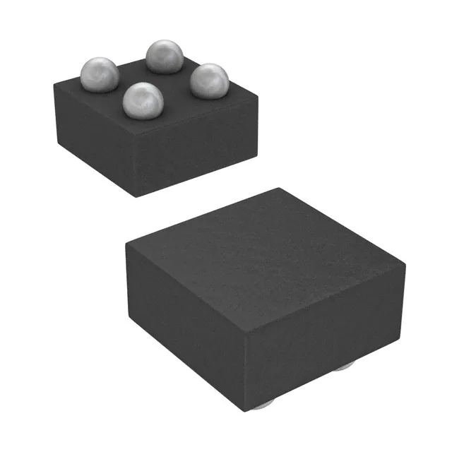
Ultra-Small 4-Terminal Wafer-Chip-Scale Package
(WCSP)
– Nominal Dimensions Shown – See Addendum
for Details
– 0.9 mm × 0.9 mm, 0.5-mm Pitch, 0.5-mm
Height (YZT)
Battery-Powered Equipment
Portable Industrial Equipment
Portable Medical Equipment
Portable Media Players
Point-of-Sale Terminal
GPS Devices
Digital Cameras
Portable Instrumentation
Smart Phones and Tablets
3 Description
The TPS22907 is a small, low RON load switch with
controlled turnon. The device contains a P-channel
MOSFET that operates over an input voltage range of
1.1 V to 3.6 V. The switch is controlled by an on and
off input (ON), which can interface directly with lowvoltage control signals.
The TPS22907 is available in a space-saving 4terminal WCSP with 0.5-mm pitch (YZT). The device
is characterized for operation over the free-air
temperature range of –40°C to 85°C.
Device Information(1)
PART NUMBER
TPS22907
PACKAGE
DSBGA (4)
BODY SIZE (NOM)
0.90 mm × 0.90 mm
(1) For all available packages, see the orderable addendum at
the end of the data sheet.
Typical Application
Power
Supply
VIN
ON
CIN
VOUT
ON
CL
RL
OFF
TPS22907
GND
GND
1
An IMPORTANT NOTICE at the end of this data sheet addresses availability, warranty, changes, use in safety-critical applications,
intellectual property matters and other important disclaimers. PRODUCTION DATA.
�TPS22907
SLVSA44B – NOVEMBER 2009 – REVISED FEBRUARY 2015
www.ti.com
Table of Contents
1
2
3
4
5
6
7
Features ..................................................................
Applications ...........................................................
Description .............................................................
Revision History.....................................................
Pin Configuration and Functions .........................
Specifications.........................................................
1
1
1
2
3
3
6.1
6.2
6.3
6.4
6.5
6.6
6.7
6.8
6.9
6.10
3
3
4
4
4
5
5
5
6
8
Absolute Maximum Ratings ......................................
ESD Ratings..............................................................
Recommended Operating Conditions.......................
Thermal Information ..................................................
Electrical Characteristics...........................................
Switching Characteristics: VIN = 3.6 V ......................
Switching Characteristics: VIN = 1.8 V ......................
Switching Characteristics: VIN = 1.1 V ......................
Typical DC Characteristics........................................
Typical AC Characteristics......................................
Parameter Measurement Information ................ 10
8
Detailed Description ............................................ 11
8.1
8.2
8.3
8.4
9
Overview .................................................................
Functional Block Diagram .......................................
Feature Description.................................................
Device Functional Modes........................................
11
11
11
11
Application and Implementation ........................ 12
9.1 Application Information............................................ 12
9.2 Typical Application ................................................. 12
10 Power Supply Recommendations ..................... 14
11 Layout................................................................... 14
11.1 Layout Guidelines ................................................. 14
11.2 Layout Example .................................................... 14
12 Device and Documentation Support ................. 15
12.1 Trademarks ........................................................... 15
12.2 Electrostatic Discharge Caution ............................ 15
12.3 Glossary ................................................................ 15
13 Mechanical, Packaging, and Orderable
Information ........................................................... 15
4 Revision History
NOTE: Page numbers for previous revisions may differ from page numbers in the current version.
Changes from Revision A (September 2013) to Revision B
•
Page
Added ESD Ratings table, Feature Description section, Device Functional Modes, Application and Implementation
section, Power Supply Recommendations section, Layout section, Device and Documentation Support section, and
Mechanical, Packaging, and Orderable Information section ................................................................................................. 3
Changes from Original (November 2009) to Revision A
Page
•
Changed Feature from: Ultra-Low ON-State Resistance to: Ultra-Low ON-State Resistance (RON) ..................................... 1
•
Changed the Feature for the Wafer-Chip-Scale Package...................................................................................................... 1
•
Changed Application from: Point Of Sales Terminal to: Point of Sale Terminal .................................................................... 1
•
Changed Application from: Smartphones to: Smartphones / Tablets .................................................................................... 1
•
Deleted the Ordering Information table .................................................................................................................................. 1
•
Changed the IIN Test Condition from: IOUT = 0 to IOUT = 0 mA................................................................................................ 4
•
Changed the IIN(OFF) Test Condition from: VON = GND to VON = 0 V ...................................................................................... 4
•
Changed the IIN(LEAKAGE) Test Condition from: VON = GND, VOUT = 0 to VON = 0 V, VOUT = 0 V ............................................. 4
•
Changed Table 1, Device Feature List................................................................................................................................. 11
2
Submit Documentation Feedback
Copyright © 2009–2015, Texas Instruments Incorporated
Product Folder Links: TPS22907
�TPS22907
www.ti.com
SLVSA44B – NOVEMBER 2009 – REVISED FEBRUARY 2015
5 Pin Configuration and Functions
YZT Package
4-Pin DSBGA
(Laser Marking View)
YZT Package
4-Pin DSBGA
(Bump View)
B
B
A
A
2
1
1
2
Pin Functions
PIN
NO.
NAME
A1
VOUT
I/O
DESCRIPTION
O
Switch output
Switch input, bypass capacitor recommended for minimizing VIN dip. See Feature Description.
A2
VIN
I
B1
GND
-—
B2
ON
I
Ground
Switch control input, active high. Do not leave floating.
6 Specifications
6.1 Absolute Maximum Ratings
over operating free-air temperature range (unless otherwise noted) (1)
MIN
MAX
UNIT
VIN
Input voltage
–0.3
4
V
VOUT
Output voltage
–0.3
(VIN + 0.3)
V
VON
Input voltage
–0.3
4
V
IMAX
Maximum continuous switch current
1
A
IPLS
Maximum pulsed current (100-µs pulse, 2% duty cycle), TA = –40°C to
+85°C
2.7
A
TJ
Maximum junction temperature
125
°C
TLEAD
Maximum lead temperature (10-s soldering time)
300
°C
Tstg
Storage temperature
150
°C
(1)
–65
Stresses beyond those listed under Absolute Maximum Ratings may cause permanent damage to the device. These are stress ratings
only, which do not imply functional operation of the device at these or any other conditions beyond those indicated under Recommended
Operating Conditions. Exposure to absolute-maximum-rated conditions for extended periods may affect device reliability.
6.2 ESD Ratings
VALUE
Human body model (HBM), per ANSI/ESDA/JEDEC JS-001, all pins
V(ESD)
(1)
(2)
Electrostatic discharge
(1)
Charged-device model (CDM), per JEDEC specification JESD22-C101, all
pins (2)
UNIT
±3000
±1000
V
JEDEC document JEP155 states that 500-V HBM allows safe manufacturing with a standard ESD control process.
JEDEC document JEP157 states that 250-V CDM allows safe manufacturing with a standard ESD control process.
Submit Documentation Feedback
Copyright © 2009–2015, Texas Instruments Incorporated
Product Folder Links: TPS22907
3
�TPS22907
SLVSA44B – NOVEMBER 2009 – REVISED FEBRUARY 2015
www.ti.com
6.3 Recommended Operating Conditions
MIN
MAX
1.1
3.6
V
VIN
V
3.6
V
VIN
Input voltage range
VOUT
Output voltage range
VIH
High-level input voltage, ON
VIL
Low-level input voltage, ON
CIN
Input capacitor
1 (1)
TA
Operating free-air temperature
–40
(1)
0.85
UNIT
0.4
V
μF
85
°C
See Application Information.
6.4 Thermal Information
TPS22907
THERMAL METRIC (1) (2)
YZT (DSBGA)
UNIT
4 PINS
RθJA
Junction-to-ambient thermal resistance
RθJC(top)
Junction-to-case(top) thermal resistance
1.9
RθJB
Junction-to-board thermal resistance
37.2
ΨJT
Junction-to-top characterization parameter
10.2
ΨJB
Junction-to-board characterization parameter
37
RθJC(bot)
Junction-to-case(bottom) thermal resistance
—
(1)
(2)
189.4
°C/W
For more information about traditional and new thermal metrics, see the IC Package Thermal Metrics application report, SPRA953
For thermal estimates of this device based on PCB copper area, see the TI PCB Thermal Calculator.
6.5 Electrical Characteristics
Unless otherwise noted, the specification applies over the operating ambient temperature -40°C ≤ TA ≤ 85°C and VIN = 1.1 V
to 3.6 V. Typical values are for VIN = 3.6 V and TA = 25°C.
TYP
MAX
IQ
Quiescent current
PARAMETER
IOUT = 0 mA, VIN = VON
TEST CONDITIONS
Full
0.07
1
µA
ISD
Off supply current
VON = 0 V, OUT = Open
Full
0.05
1
µA
IIN(LEAKAGE)
Leakage current
VON = 0 V, VOUT = 0 V
Full
0.05
1
µA
25°C
44
60
VIN = 3.6 V, IOUT = –200 mA
VIN = 2.5 V, IOUT = –200 mA
RON
ON-state resistance
VIN = 1.8 V, IOUT = –200 mA
VIN = 1.2 V, IOUT = –200 mA
VIN = 1.1 V, IOUT = –200 mA
ION
4
ON input leakage current
VON = 0 V to 3.6 V
Submit Documentation Feedback
TA
MIN
Full
25°C
67
50
Full
25°C
83
mΩ
106
117
97
Full
Full
72
80
Full
25°C
63
70
58
Full
25°C
UNIT
125
140
0.005
1
µA
Copyright © 2009–2015, Texas Instruments Incorporated
Product Folder Links: TPS22907
�TPS22907
www.ti.com
SLVSA44B – NOVEMBER 2009 – REVISED FEBRUARY 2015
6.6 Switching Characteristics: VIN = 3.6 V
TA = 25°C (unless otherwise noted)
PARAMETER
TEST CONDITIONS
MIN
TYP
MAX
UNIT
tON
Turn-ON time
RL = 500 Ω, CL = 0.1 μF
28
μs
tOFF
Turn-OFF time
RL = 500 Ω, CL = 0.1 μF
40
μs
tr
VOUT rise time
RL = 500 Ω, CL = 0.1 μF
25
μs
tf
VOUT fall time
RL = 500 Ω, CL = 0.1 μF
116
μs
6.7 Switching Characteristics: VIN = 1.8 V
TA = 25°C (unless otherwise noted)
PARAMETER
TEST CONDITIONS
MIN
TYP
MAX
UNIT
tON
Turn-ON time
RL = 500 Ω, CL = 0.1 μF
48
μs
tOFF
Turn-OFF time
RL = 500 Ω, CL = 0.1 μF
40
μs
tr
VOUT rise time
RL = 500 Ω, CL = 0.1 μF
36
μs
tf
VOUT fall time
RL = 500 Ω, CL = 0.1 μF
113
μs
6.8 Switching Characteristics: VIN = 1.1 V
TA = 25°C (unless otherwise noted)
PARAMETER
TEST CONDITIONS
MIN
TYP
MAX
UNIT
tON
Turn-ON time
RL = 500 Ω, CL = 0.1 μF
81
μs
tOFF
Turn-OFF time
RL = 500 Ω, CL = 0.1 μF
42
μs
tr
VOUT rise time
RL = 500 Ω, CL = 0.1 μF
57
μs
tf
VOUT fall time
RL = 500 Ω, CL = 0.1 μF
113
μs
Submit Documentation Feedback
Copyright © 2009–2015, Texas Instruments Incorporated
Product Folder Links: TPS22907
5
�TPS22907
SLVSA44B – NOVEMBER 2009 – REVISED FEBRUARY 2015
www.ti.com
6.9 Typical DC Characteristics
0.14
0.06
V IN = 3.6 V
IOUT = 200 m A
IOUT = -200 m A
0.05
r ON - ON-State Resistance - W
ð
W
r ON - ON-State Resistance - W
0.12
0.1
0.08
TA = 85°C
0.06
0.04
TA = 25°C
TA = -40°C
0.04
0.03
0.02
0.01
0.02
0
1
1.5
2
2.5
3
3.5
0
-40
4
-15
V IN - Input Voltage - V
Figure 1. ON-State Resistance vs. Input Voltage
85
V IN = 3.6 V
IOUT = 0
V IN = V ON
0.25
IIN - Quiescent Current - µA
0.20
IIN - Quiescent Current - µA
60
0.30
V ON = V IN
IOUT = 0
0.15
0.10
0.05
0.20
0.15
0.10
0.05
0.00
-40
0.00
1
1.5
2
2.5
3
3.5
4
-15
V IN - Input Voltage - V
10
35
60
85
TA - Tem perature - °C
Figure 3. VIN Quiescent Current vs. Input Voltage
Figure 4. VIN Quiescent Current vs. Temperature
0.14
0.12
V IN = 3.6 V
V ON = 0 V
0.12
IIN(OFF) - Off Supply Current - µA
0.10
IIN(off) - Off Supply Current - µA
35
Figure 2. ON-State Resistance vs. Temperature
0.25
0.08
0.06
0.04
0.02
0.10
0.08
0.06
0.04
0.02
0.00
1
1.5
2
2.5
3
3.5
0.00
-40
4
-15
10
35
60
85
TA - Tem perature - °C
V IN - Input Voltage - V
Figure 5. VIN Off Supply Current vs. Input Voltage
6
10
TA - Tem perature - °C
Figure 6. VIN OFF Supply Current vs. Temperature
Submit Documentation Feedback
Copyright © 2009–2015, Texas Instruments Incorporated
Product Folder Links: TPS22907
�TPS22907
www.ti.com
SLVSA44B – NOVEMBER 2009 – REVISED FEBRUARY 2015
Typical DC Characteristics (continued)
0.50
0.18
IOUT = 0
V ON = 0
V IN = 3.6 V
IOUT = 0
V ON = 0
0.45
0.40
0.14
IIN(leakage) - Leakage Current - µA
IIN(leakage) - Leakage Current - µA
0.16
0.12
0.10
0.08
0.06
0.04
0.02
0.35
0.30
0.25
0.20
0.15
0.10
0.05
0.00
1
1.5
2
2.5
3
3.5
0.00
-40
4
-15
10
35
60
85
TA - Tem perature - °C
V IN - Input Voltage - V
Figure 7. VIN Leakage Current vs. Input Voltage
Figure 8. VIN Leakage Current vs. Temperature
4.0
3.5
V OUT - Output Voltage - V
3.0
TA = 85°C
2.5
TA = 25°C
2.0
TA = -40C
1.5
1.0
V IN = 3.6 V
IOUT = 500 m A
0.5
0.0
0
0.5
1
1.5
2
V ON - ON Voltage - V
Figure 9. ON Input Threshold
Submit Documentation Feedback
Copyright © 2009–2015, Texas Instruments Incorporated
Product Folder Links: TPS22907
7
�TPS22907
SLVSA44B – NOVEMBER 2009 – REVISED FEBRUARY 2015
www.ti.com
6.10 Typical AC Characteristics
41.0
40
V IN = 3.6 V
CL = 0.1 µF
RL = 500 W
40.5
30
39.5
t ON - On Time - µs
t OFF - Off Time - µs
40.0
39.0
38.5
38.0
25
20
15
10
37.5
5
37.0
36.5
-40
V IN = 3.6 V
CL = 0.1 µF
RL = 500 W
35
-15
10
35
60
0
-40
85
-15
TA - Tem perature - °C
Figure 10. OFF Time vs. Temperature
60
85
122
V IN = 3.6 V
CL = 0.1 µF
RL = 500 W
30.0
V IN = 3.6 V
CL = 0.1 µF
RL = 500 W
120
118
t f - Fall Time - µs
29.5
t r - Rise Time - µs
35
Figure 11. ON Time vs. Temperature
30.5
29.0
28.5
28.0
116
114
112
27.5
110
27.0
108
26.5
-40
10
TA - Tem perature - °C
-15
10
35
60
106
-40
85
TA - Tem perature - °C
-15
10
35
60
85
TA - Tem perature - °C
Figure 12. Rise Time vs. Temperature
Figure 13. Fall Time vs. Temperature
IOUT
VON
VON
VIN = 3.6 V
CIN = 1 µF
CL = 0.1 µF
RL = 36 W
TA = 25°C
IOUT
VIN = 3.6 V
CIN = 1 µF
CL = 0.1 µF
RL = 36 W
TA = 25°C
Figure 14. tON Response
8
Figure 15. tOFF Response
Submit Documentation Feedback
Copyright © 2009–2015, Texas Instruments Incorporated
Product Folder Links: TPS22907
�TPS22907
www.ti.com
SLVSA44B – NOVEMBER 2009 – REVISED FEBRUARY 2015
Typical AC Characteristics (continued)
IOUT
VON
VON
IOUT
VIN = 1.1 V
CIN = 1 µF
CL = 0.1 µF
RL = 11 W
TA = 25°C
VIN = 1.1 V
CIN = 1 µF
CL = 0.1 µF
RL = 11 W
TA = 25°C
Figure 16. tON Response
Figure 17. tOFF Response
IOUT
VON
VON
IOUT
VIN = 3.6 V
CIN = 1 µF
CL = 10 µF
RL = 36 W
TA = 25°C
Figure 18. tON Response
Figure 19. tOFF Response
IOUT
VON
VON
IOUT
VIN = 3.6 V
CIN = 1 µF
CL = 10 µF
RL = 36 W
TA = 25°C
VIN = 1.1 V
CIN = 1 µF
CL = 10 µF
RL = 11 W
TA = 25°C
VIN = 1.1 V
CIN = 1 µF
CL = 10 µF
RL = 11 W
TA = 25°C
Figure 20. tON Response
Figure 21. tOFF Response
Submit Documentation Feedback
Copyright © 2009–2015, Texas Instruments Incorporated
Product Folder Links: TPS22907
9
�TPS22907
SLVSA44B – NOVEMBER 2009 – REVISED FEBRUARY 2015
www.ti.com
7 Parameter Measurement Information
VIN
VOUT
CIN = 1µF
ON
+
-
(A)
CL
ON
RL
OFF
GND
TPS22907
GND
GND
TEST CIRCUIT
VON
50%
50%
tOFF
tON
VOUT
50%
50%
tf
tr
90%
VOUT
10%
90%
10%
tON/tOFF WAVEFORMS
(A) Control signal rise and fall times are 100 ns.
Figure 22. Test Circuit and tON/tOFF Waveforms
10
Submit Documentation Feedback
Copyright © 2009–2015, Texas Instruments Incorporated
Product Folder Links: TPS22907
�TPS22907
www.ti.com
SLVSA44B – NOVEMBER 2009 – REVISED FEBRUARY 2015
8 Detailed Description
8.1 Overview
The TPS22907 is a single-channel, 1-A load switch in a small, space-saving DSBGA-4 package. This device
implements a P-channel MOSFET to provide a low ON-resistance for a low-voltage drop across the device. A
controlled rise time is used in applications to limit the inrush current.
8.2 Functional Block Diagram
VIN
ON
A2
B2
Control
Logic
A1
VOUT
B1
GND
8.3 Feature Description
Table 1. Device Feature List
DEVICE
RON (Typical)
VIN = 1.8 V
SLEW RATE (Typical)
VIN = 1.8 V
MAXIMUM OUTPUT
CURRENT
ENABLE
TPS22907
58 mΩ
36 μs
1A
Active high
8.3.1 On and Off Control
The ON pin controls the state of the switch. Asserting ON high enables the switch. ON is active high and has a
low threshold, making it capable of interfacing with low-voltage signals. The ON pin is compatible with standard
GPIO logic threshold. It can be used with any microcontroller with 1.2-V, 1.8-V, 2.5-V, or 3.3-V GPIOs.
8.4 Device Functional Modes
Table 2. Function Table
ON (Control Input)
VIN to VOUT
L
OFF
H
ON
Submit Documentation Feedback
Copyright © 2009–2015, Texas Instruments Incorporated
Product Folder Links: TPS22907
11
�TPS22907
SLVSA44B – NOVEMBER 2009 – REVISED FEBRUARY 2015
www.ti.com
9 Application and Implementation
NOTE
Information in the following applications sections is not part of the TI component
specification, and TI does not warrant its accuracy or completeness. TI’s customers are
responsible for determining suitability of components for their purposes. Customers should
validate and test their design implementation to confirm system functionality.
9.1 Application Information
9.1.1 Input Capacitor
To limit the voltage drop on the input supply caused by transient inrush currents when the switch turns on into a
discharged load capacitor, a capacitor needs to be placed between VIN and GND. A 1-μF ceramic capacitor, CIN,
place close to the pins is usually sufficient. Higher values of CIN can be use to further reduce the voltage drop
during high-current application. When switching heavy loads, TI recommends having an input capacitor
approximately ten times higher than the output capacitor to avoid excessive voltage drop.
9.1.2 Output Capacitor
Due to the integrated body diode in the PMOS switch, a CIN greater than CL is highly recommended. A CL
greater than CIN can cause VOUT to exceed VIN when the system supply is removed. This could result in current
flow through the body diode from VOUT to VIN. A CIN to CL ratio of at least 10 to 1 is recommended for minimizing
VIN dip caused by inrush currents during startup; however, a 10 to 1 ratio for capacitance is not required for
proper functionality of the device. A ratio smaller than 10 to 1 (such as 1 to 1) could cause slightly more VIN dip
at turnon due to inrush currents.
9.2 Typical Application
Power
Supply
VOUT
VIN
ON
CIN
ON
CL
RL
OFF
GND
TPS22907
GND
Figure 23. Typical Application Schematic
9.2.1 Design Requirements
Table 3 lists the design requirements for the device.
Table 3. Design Parameters
DESIGN PARAMETER
12
EXAMPLE VALUE
VIN
3.6 V
CL
4.7 µF
Load current
1A
Ambient Temperature
25 °C
Maximum inrush current
750 mA
Submit Documentation Feedback
Copyright © 2009–2015, Texas Instruments Incorporated
Product Folder Links: TPS22907
�TPS22907
www.ti.com
SLVSA44B – NOVEMBER 2009 – REVISED FEBRUARY 2015
9.2.2 Detailed Design Procedure
9.2.2.1 Managing Inrush Current
When the switch is enabled, the output capacitors must be charged up from 0 V to the set value (3.6 V in this
example). This charge arrives in the form of inrush current. Inrush current can be calculated using the following
equation:
dV
IINRUSH = CL ´ OUT
dt
where:
•
•
•
CL = Output capacitance
dVOUT = Output voltage
dt = Rise time
(1)
The TPS22907 offers a controlled rise time for minimizing inrush current. This device can be selected based
upon the minimum acceptable rise time which can be calculated using the design requirements and the inrush
current equation. An output capacitance of 4.7 µF will be used because the amount of inrush current increases
with output capacitance:
750 mA = 4.7 µF × 3.6 V / dt
where
•
dt = 22.56 µs
(2)
To ensure an inrush current of less than 750 mA, a device with a rise time greater than 22.56 µs must be used.
The TPS22907 has a typical rise time of 25 µs at 3.6 V which meets the above design requirements.
9.2.2.2 Voltage Drop from VIN to VOUT
The voltage drop from VIN to VOUT is determined by the ON-resistance of the device and the load current. RON
can be found in Electrical Characteristics and is dependent on temperature. When the value of RON is found, the
following equation can be used to calculate the voltage drop across the device:
ΔV = ILOAD × RON
where:
•
•
•
ΔV = Voltage drop across the device
ILOAD = Load current
RON = ON-resistance of the device
(3)
At VIN = 3.6 V, the TPS22907 has an RON value of 44 mΩ. Using this value and the defined load current, the
above equation can be evaluated:
ΔV = 1 A × 44 mΩ
ΔV = 44 mV
(4)
Therefore, the voltage drop across the device will be 44 mV.
Submit Documentation Feedback
Copyright © 2009–2015, Texas Instruments Incorporated
Product Folder Links: TPS22907
13
�TPS22907
SLVSA44B – NOVEMBER 2009 – REVISED FEBRUARY 2015
www.ti.com
9.2.3 Application Curve
Figure 24 shows the inrush current expected for different load capacitances at varying VIN voltages.
1600
VIN = 3.6V
VIN = 1.8V
VIN = 1.1V
1400
Inrush Current (mA)
1200
1000
800
600
400
200
0
0
1
2
3
4
5
6
CL (PF)
7
8
9
10
A001
Figure 24. Expected Inrush Current vs Load Capacitance
10 Power Supply Recommendations
The device is designed to operate with a VIN voltage range of 1.1 V to 3.6 V. The power supply should be well
regulated and placed as close to the device terminals as possible. It must be able to withstand all transient and
load current steps. In most situations, using the minimum recommended input capacitance of 1 uF is sufficient to
prevent the supply voltage from dipping when the switch is turned on. In cases where the power supply is slow
to respond to a large transient current or large load current step, additional bulk capacitance may be required on
the input.
11 Layout
11.1 Layout Guidelines
For best performance, VIN and VOUT traces should be as short and wide as possible to help minimize the
parasitic electrical effects. To be most effective, the input and output capacitors should be placed close to the
device to minimize the effects that parasitic trace inductances may have on normal operation.
11.2 Layout Example
Figure 25. Example Layout for the TPS22907
14
Submit Documentation Feedback
Copyright © 2009–2015, Texas Instruments Incorporated
Product Folder Links: TPS22907
�TPS22907
www.ti.com
SLVSA44B – NOVEMBER 2009 – REVISED FEBRUARY 2015
12 Device and Documentation Support
12.1 Trademarks
All trademarks are the property of their respective owners.
12.2 Electrostatic Discharge Caution
These devices have limited built-in ESD protection. The leads should be shorted together or the device placed in conductive foam
during storage or handling to prevent electrostatic damage to the MOS gates.
12.3 Glossary
SLYZ022 — TI Glossary.
This glossary lists and explains terms, acronyms, and definitions.
13 Mechanical, Packaging, and Orderable Information
The following pages include mechanical, packaging, and orderable information. This information is the most
current data available for the designated devices. This data is subject to change without notice and revision of
this document. For browser-based versions of this data sheet, refer to the left-hand navigation.
Submit Documentation Feedback
Copyright © 2009–2015, Texas Instruments Incorporated
Product Folder Links: TPS22907
15
�PACKAGE OPTION ADDENDUM
www.ti.com
10-Dec-2020
PACKAGING INFORMATION
Orderable Device
Status
(1)
Package Type Package Pins Package
Drawing
Qty
Eco Plan
(2)
Lead finish/
Ball material
MSL Peak Temp
Op Temp (°C)
Device Marking
(3)
(4/5)
(6)
TPS22907YZTR
NRND
DSBGA
YZT
4
3000
RoHS & Green
SNAGCU
Level-1-260C-UNLIM
-40 to 85
5K
(F, G)
TPS22907YZTT
NRND
DSBGA
YZT
4
250
RoHS & Green
SNAGCU
Level-1-260C-UNLIM
-40 to 85
5K
(F, G)
(1)
The marketing status values are defined as follows:
ACTIVE: Product device recommended for new designs.
LIFEBUY: TI has announced that the device will be discontinued, and a lifetime-buy period is in effect.
NRND: Not recommended for new designs. Device is in production to support existing customers, but TI does not recommend using this part in a new design.
PREVIEW: Device has been announced but is not in production. Samples may or may not be available.
OBSOLETE: TI has discontinued the production of the device.
(2)
RoHS: TI defines "RoHS" to mean semiconductor products that are compliant with the current EU RoHS requirements for all 10 RoHS substances, including the requirement that RoHS substance
do not exceed 0.1% by weight in homogeneous materials. Where designed to be soldered at high temperatures, "RoHS" products are suitable for use in specified lead-free processes. TI may
reference these types of products as "Pb-Free".
RoHS Exempt: TI defines "RoHS Exempt" to mean products that contain lead but are compliant with EU RoHS pursuant to a specific EU RoHS exemption.
Green: TI defines "Green" to mean the content of Chlorine (Cl) and Bromine (Br) based flame retardants meet JS709B low halogen requirements of