TPS22916
TPS22916
SLVSDO5E – JULY 2017 – REVISED SEPTEMBER
2020
SLVSDO5E – JULY 2017 – REVISED SEPTEMBER 2020
www.ti.com
TPS22916xx 1-V – 5.5-V, 2-A, 60-mΩ Ultra-Low Leakage Load Switch
1 Features
3 Description
•
•
•
The TPS22916xx is a small, single channel load
switch using a low leakage P-Channel MOSFET for
minimum power loss. Advanced gate control design
supports operating voltages as low as 1 V with
minimal increase in ON-Resistance and power loss.
•
•
•
•
•
•
•
Input Operating Voltage Range (VIN): 1 V–5.5 V
Maximum Continuous Current (IMAX): 2 A
ON-Resistance (RON):
– 5 VIN = 60 mΩ (typ), 100 mΩ (85°C max)
– 1.8 VIN = 100 mΩ (typ), 150 mΩ (85°C max)
– 1 VIN = 200 mΩ (typ), 325 mΩ (85°C max)
Ultra-Low Power Consumption:
– ON State (IQ): 0.5 µA (typ), 1 µA (max)
– OFF State (ISD): 10 nA (typ), 100 nA (max)
– TPS22916CL (ISD): 100 nA (typ), 300 nA (max)
Smart ON Pin Pull Down (RPD):
– ON ≥ VIH (ION): 10 nA (max)
– ON ≤ VIL (RPD): 750 kΩ (typ)
Slow Timing in C Version Limits Inrush Current:
– 5-V Turnon time (tON): 1400 µs at 5 mV/µs
– 1.8-V Turnon time (tON): 3000 µs at 1 mV/µs
– 1-V Turnon time (tON): 6500 µs at 0.3 mV/µs
Fast Timing in B Version Reduces Wait Time:
– 5-V Turnon time (tON): 115 µs at 57 mV/µs
– 1.8-V Turnon time (tON): 250 µs at 12 mV/µs
– 1-V Turnon time (tON): 510 µs at 3.3 mV/µs
Always-ON True Reverse Current Blocking (RCB):
– Activation Current (IRCB): –500 mA (typ)
– Reverse Leakage (IIN,RCB): –300 nA (max)
Quick Output Discharge (QOD): 150 Ω (typ)
(N version has no QOD)
Active Low Enable Option (L Version)
2 Applications
•
•
•
•
Multiple timing options are available to support
various system loading conditions. For heavy
capacitive loads, the slow turnon timing in the C
version minimizes the inrush current. In cases with
light capacitive loads, the fast timing in the B version
reduces required wait time.
The switch ON state is controlled by a digital input
that is capable of interfacing directly with low-voltage
control signals. Both Active High and Active Low (L)
versions are available. When power is first applied, a
Smart Pull Down is used to keep the ON pin from
floating until system sequencing is complete. Once
the ON pin is deliberately driven high (≥VIH), the
Smart Pull Down is disconnected to prevent
unnecessary power loss.
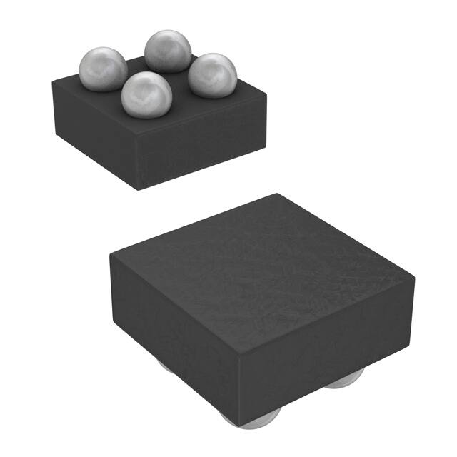
The TPS22916xx is available in a small, space saving
0.78 mm × 0.78 mm, 0.4-mm pitch, 0.5-mm height 4pin Wafer-Chip-Scale (WCSP) package (YFP). The
device is characterized for operation over a
temperature range of –40°C to +85°C.
Device Information (1)
PART NUMBER
TPS22916xx
(1)
Wearables
Smartphones
Tablets
Portable Speakers
BODY SIZE (NOM)
0.78 mm × 0.78 mm
For all available packages, see the orderable addendum at
the end of the data sheet.
Device Comparison Table
TIMING
QOD
ENABLE (ON)
TPS22916B
VERSION
Fast
Yes
Active High
TPS22916C
Slow
Yes
Active High
TPS22916CN
Slow
No
Active High
TPS22916CL
Slow
Yes
Active Low
VIN
VIN
PACKAGE
WCSP (4)
+
VOUT
CIN
CL
±
H
L
RL
GND
ON
TPS22916xx
Copyright © 2017, Texas Instruments Incorporated
Simplified Schematic
An IMPORTANT NOTICE at the end of this data sheet addresses availability, warranty, changes, use in safety-critical applications,
Submit Document Feedback
Copyright
© 2020 Texas
Instruments
Incorporated
intellectual
property
matters
and other important disclaimers. PRODUCTION DATA.
Product Folder Links: TPS22916
1
�TPS22916
www.ti.com
SLVSDO5E – JULY 2017 – REVISED SEPTEMBER 2020
Table of Contents
1 Features............................................................................1
2 Applications..................................................................... 1
3 Description.......................................................................1
4 Revision History.............................................................. 2
5 Pin Configuration and Functions...................................3
6 Specifications.................................................................. 4
6.1 Absolute Maximum Ratings........................................ 4
6.2 ESD Ratings............................................................... 4
6.3 Recommended Operating Conditions.........................4
6.4 Thermal Information....................................................4
6.5 Electrical Characteristics.............................................5
6.6 Switching Characteristics............................................6
6.7 Typical Characteristics................................................ 8
7 Parameter Measurement Information.......................... 15
8 Detailed Description......................................................16
8.1 Overview................................................................... 16
8.2 Functional Block Diagram......................................... 16
8.3 Feature Description...................................................16
8.4 Device Functional Modes..........................................17
9 Application and Implementation.................................. 18
9.1 Application Information............................................. 18
10 Power Supply Recommendations..............................19
11 Layout........................................................................... 20
11.1 Layout Guidelines................................................... 20
11.2 Layout Example...................................................... 20
11.3 Thermal Considerations.......................................... 20
12 Device and Documentation Support..........................21
12.1 Documentation Support.......................................... 21
12.2 Receiving Notification of Documentation Updates..21
12.3 Support Resources................................................. 21
12.4 Trademarks............................................................. 21
12.5 Electrostatic Discharge Caution..............................21
12.6 Glossary..................................................................21
13 Mechanical, Packaging, and Orderable
Information.................................................................... 21
13.1 Package Option Addendum.................................... 22
4 Revision History
NOTE: Page numbers for previous revisions may differ from page numbers in the current version.
Changes from Revision D (October 2019) to Revision E (September 2020)
Page
• Updated the numbering format for tables, figures and cross-references throughout the document...................1
Changes from Revision C (October 2018) to Revision D (October 2019)
Page
• Changed package dimensions from 0.74 mm x 0.74 mm to 0.78 mm x 0.78 mm..............................................1
Changes from Revision B (December 2017) to Revision C (October 2018)
Page
• Changed Package Drawing Dimensions ......................................................................................................... 21
Changes from Revision A (September 2017) to Revision B (December 2017)
Page
• Changed Pinout drawing labeled Laser Marking................................................................................................ 1
Changes from Revision * (July 2017) to Revision A (September 2017)
Page
• Changed device document from Advanced Info to Production Data ................................................................. 1
2
Submit Document Feedback
Copyright © 2020 Texas Instruments Incorporated
Product Folder Links: TPS22916
�TPS22916
www.ti.com
SLVSDO5E – JULY 2017 – REVISED SEPTEMBER 2020
5 Pin Configuration and Functions
B
A
ON
GND
VIN
VOUT
2
B
A
GND
ON
VOUT
VIN
1
1
Figure 5-1. YFP Package 4-Pin WSON Laser
Marking View
2
Figure 5-2. YFP Package 4-Pin WSON Bump View
TPS22916xx Pin Functions
PIN
NO.
NAME
A1
VOUT
TYPE
DESCRIPTION
Power
Switch output
A2
VIN
Power
Switch input
B1
GND
Ground
Device ground
B2
ON
Digital input
Device enable
Submit Document Feedback
Copyright © 2020 Texas Instruments Incorporated
Product Folder Links: TPS22916
3
�TPS22916
www.ti.com
SLVSDO5E – JULY 2017 – REVISED SEPTEMBER 2020
6 Specifications
6.1 Absolute Maximum Ratings
Over operating free-air temperature range (unless otherwise noted)(1)
MIN
MAX
UNIT
VIN
Input voltage
–0.3
6
V
VOUT
Output voltage
–0.3
6
V
VON
Enable voltage
–0.3
6
V
IMAX
Maximum continuous switch current
IPLS
Maximum pulsed switch current, pulse < 300-µs, 2% duty cycle
TJ,MAX
Maximum junction temperature
TSTG
Storage temperature
TLEAD
Maximum Lead temperature (10-s soldering time)
(1)
–65
2
A
2.5
A
125
°C
150
°C
300
°C
Stresses beyond those listed under Absolute Maximum Ratings may cause permanent damage to the device. These are stress ratings
only, which do not imply functional operation of the device at these or any other conditions beyond those indicated under
Recommended Operating Conditions. Exposure to absolute-maximum-rated conditions for extended periods may affect device
reliability.
6.2 ESD Ratings
VALUE
Human-body model (HBM), per ANSI/ESDA/JEDEC
V(ESD)
(1)
(2)
Electrostatic discharge
JS-001(1)
UNIT
±2000
Charged-device model (CDM), per JEDEC specification JESD22C101(2)
V
±500
JEDEC document JEP155 states that 500-V HBM allows safe manufacturing with a standard ESD control process. Manufacturing with
less than 500-V HBM is possible with the necessary precautions. Pins listed as ±2000 V may actually have higher performance.
JEDEC document JEP157 states that 250-V CDM allows safe manufacturing with a standard ESD control process. Manufacturing with
less than 250-V CDM is possible with the necessary precautions. Pins listed as ±500 V may actually have higher performance.
6.3 Recommended Operating Conditions
Over operating free-air temperature range (unless otherwise noted)
MIN
MAX
VIN
Input voltage
1
5.5
V
VOUT
Output voltage
0
5.5
V
VIH
High-level input voltage, ON
1
5.5
V
0
0.35
V
–40
85
°C
VIL
Low-level input voltage, ON
TA
Operating free-air temperature
UNIT
6.4 Thermal Information
TPS22916xx
Thermal
Parameters(1)
YFP (WCSP)
UNIT
4 PINS
θJA
Junction-to-ambient thermal resistance
193
°C/W
θJCtop
Junction-to-case (top) thermal resistance
2.3
°C/W
θJB
Junction-to-board thermal resistance
36
°C/W
ψJT
Junction-to-top characterization parameter
12
°C/W
ψJB
Junction-to-board characterization parameter
36
°C/W
(1)
4
For more information about traditional and new thermal metrics, see the Semiconductor and IC Package Thermal Metrics application
report.
Submit Document Feedback
Copyright © 2020 Texas Instruments Incorporated
Product Folder Links: TPS22916
�TPS22916
www.ti.com
SLVSDO5E – JULY 2017 – REVISED SEPTEMBER 2020
6.5 Electrical Characteristics
Unless otherwise noted, the specification in the following table applies for all variants over the entire
recommended power supply voltage range of 1 V to 5.5 V unless noted otherwise. Typical Values are at 25°C.
PARAMETER
TEST CONDITIONS
TJ
MIN
TYP MAX
UNIT
INPUT SUPPLY (VIN)
IQ,VIN
VIN Quiescent current
Enabled, VOUT = Open
–40°C to +85°C
0.5
1.0
µA
ISD,VIN
VIN Shutdown current
Disabled, VOUT = GND
(TPS22916B/C/CN)
–40°C to +85°C
10
100
nA
Disabled, VOUT = GND (TPS22916CL)
–40°C to +85°C
100
300
nA
ON-RESISTANCE
(RON)
25°C
VIN = 5 V
60
–40°C to +85°C
–40°C to +105°C
120
25°C
VIN = 3.6 V
70
ON-Resistance
IOUT = 200 mA
VIN = 1.8 V
120
–40°C to +105°C
140
100
–40°C to +85°C
mΩ
175
25°C
150
200
–40°C to +85°C
250
–40°C to +105°C
300
25°C
VIN = 1 V
125
150
–40°C to +105°C
VIN = 1.2 V
90
–40°C to +85°C
25°C
RON
80
100
200
275
–40°C to +85°C
325
–40°C to +105°C
375
ENABLE PIN (ON)
ION
ON Pin leakage
Enabled
–40°C to +85°C
RPD
Smart Pull Down Resistance
Disabled
–40°C to +85°C
–10
750
10
kΩ
nA
mA
REVERSE CURRENT BLOCKING
(RCB)
IRCB
RCB Activation Current
Enabled, VOUT > VIN
–40°C to +85°C
-500
tRCB
RCB Activation time
Enabled, VOUT > VIN + 200mV
–40°C to +85°C
10
µs
VRCB
RCB Release Voltage
Enabled, VOUT > VIN
–40°C to +85°C
25
mV
IIN,RCB
VIN Reverse Leakage Current
0 V ≤ VIN + VRCB ≤ VOUT ≤ 5.5 V
–40°C to +85°C
Disabled (Not in TPS22916CN)
–40°C to +85°C
–300
nA
QUICK OUTPUT DISCHARGE
(QOD)
QOD(1)
(1)
Output discharge resistance
150
Ω
For more information on which devices include quick output discharge, see the Device Functional Modes section.
Submit Document Feedback
Copyright © 2020 Texas Instruments Incorporated
Product Folder Links: TPS22916
5
�TPS22916
www.ti.com
SLVSDO5E – JULY 2017 – REVISED SEPTEMBER 2020
6.6 Switching Characteristics
Unless otherwise noted, the typical characteristics in the following table applies over the entire recommended
power supply voltage range of 1 V to 5.5 V at 25°C with a load of CL = 0.1µF, RL = 10Ω.
PARAMETER
TEST CONDITIONS
MIN
TYP
MAX
UNIT
TPS22916B
tON
tRISE
SRON
tOFF
Turn On Time
Rise Time
Slew Rate
Turn Off Time
VIN = 5 V
115
VIN = 3.6 V
140
VIN = 1.8 V
250
VIN = 1.2 V
350
VIN = 1 V
510
VIN = 5 V
70
VIN = 3.6 V
80
VIN = 1.8 V
130
VIN = 1.2 V
190
VIN = 1 V
240
VIN = 5 V
57
VIN = 3.6 V
36
VIN = 1.8 V
12
VIN = 1.2 V
5.1
VIN = 1 V
3.3
VIN = 5 V
5
VIN = 3.6 V
5
VIN = 1.8 V
10
VIN = 1.2 V
15
VIN = 1 V
tFALL
6
Fall Time
CL = 0.1 µF, RL = 10
µs
µs
mV/µs
µs
25
Ω(1)
CL = 1µF, RL = Open(1)
Submit Document Feedback
2.3
315
µs
Copyright © 2020 Texas Instruments Incorporated
Product Folder Links: TPS22916
�TPS22916
www.ti.com
SLVSDO5E – JULY 2017 – REVISED SEPTEMBER 2020
6.6 Switching Characteristics (continued)
Unless otherwise noted, the typical characteristics in the following table applies over the entire recommended
power supply voltage range of 1 V to 5.5 V at 25°C with a load of CL = 0.1µF, RL = 10Ω.
PARAMETER
TEST CONDITIONS
MIN
TYP
MAX
UNIT
TPS22916C, TPS22916CN, TPS22916CL
tON
Turn On Time
tRISE
Rise Time
SRON
tOFF
tFALL
(1)
(2)
Slew Rate
Turn Off Time
Fall Time(2)
VIN = 5 V
1400
VIN = 3.6 V
1700
VIN = 1.8 V
3000
VIN = 1.2 V
5000
VIN = 1 V
6500
VIN = 5 V
800
VIN = 3.6 V
900
VIN = 1.8 V
1400
VIN = 1.2 V
2300
VIN = 1 V
3000
VIN = 5 V
5
VIN = 3.6 V
3.2
VIN = 1.8 V
1
VIN = 1.2 V
0.4
VIN = 1 V
0.3
VIN = 5 V
5
VIN = 3.6 V
5
VIN = 1.8 V
10
VIN = 1.2 V
15
VIN = 1 V
25
CL = 0.1 µF, RL = 10 Ω(1)
2.3
CL = 10µF, RL = Open(1)
3150
µs
µs
mV/µs
µs
µs
See the Fall Time (tFALL) and Quick Output Discharge (QOD) section for information on how RL and CL affect Fall Time.
Devices without Quick Output Discharge (QOD) may not discharge completely.
Submit Document Feedback
Copyright © 2020 Texas Instruments Incorporated
Product Folder Links: TPS22916
7
�TPS22916
www.ti.com
SLVSDO5E – JULY 2017 – REVISED SEPTEMBER 2020
6.7 Typical Characteristics
6.7.1 Typical Electrical Characteristics
The typical characteristics curves in this section apply to all devices unless otherwise noted.
220
220
1V
1.2 V
1.8 V
200
180
3.6 V
5V
180
160
RON (m:)
160
RON (m:)
105qC
85qC
25qC
40qC
200
140
120
140
120
100
100
80
80
60
60
40
-40
40
-20
0
20
40
60
Temperature (°C)
80
100
120
1
1.5
2
2.5
D004
Enabled
3
3.5
VIN (V)
4
4.5
5
5.5
D003
Enabled
Figure 6-1. ON-Resistance vs Temperature
Figure 6-2. ON-Resistance vs Input voltage
50
250
85qC
25qC
40qC
45
40
200
ISD,VIN (nA)
ISD,VIN (nA)
35
30
25
20
150
100
15
10
50
85°C
15°C
40°C
5
0
0
1
1.5
2
2.5
3
3.5
VIN (V)
4
4.5
5
5.5
1
TPS22916C, TPS22916CN, TPS22916B
VON ≤ VIL
Figure 6-3. Shutdown Current
2.5
3
3.5
VIN (V)
4
4.5
5
5.5
D015
VON ≥ VIH
Figure 6-4. Shutdown Current (Active Low)
800
0.72
750
0.7
700
0.68
VIH
VIL
0.66
600
VON (V)
IQ,VIN (nA)
2
TPS22916CL
650
550
500
0.64
0.62
0.6
450
400
0.58
85qC
25qC
40qC
350
0.56
300
0.54
1
1.5
2
2.5
3
3.5
VIN (V)
4
4.5
5
5.5
1
1.5
D001
Enabled
2
2.5
3
3.5
VIN (V)
4
4.5
5
5.5
D006
–40°C to +85°C
Figure 6-5. Quiescent Current
8
1.5
D002
Figure 6-6. ON Pin Threshold
Submit Document Feedback
Copyright © 2020 Texas Instruments Incorporated
Product Folder Links: TPS22916
�TPS22916
www.ti.com
SLVSDO5E – JULY 2017 – REVISED SEPTEMBER 2020
260
1050
1000
85qC
25qC
40qC
240
220
900
QOD (:)
RPD (k:)
950
850
800
200
180
750
160
700
650
-40
140
-20
0
20
40
Temperature (qC)
60
80
100
1
1.5
D005
VON ≤ VIL
TPS22916C
Figure 6-7. ON Pin Smart Pull Down
2
2.5
3
3.5
VIN (V)
TPS22916CL
4
4.5
5
5.5
D007
TPS22916B
Figure 6-8. Quick Output Discharge
Submit Document Feedback
Copyright © 2020 Texas Instruments Incorporated
Product Folder Links: TPS22916
9
�TPS22916
www.ti.com
SLVSDO5E – JULY 2017 – REVISED SEPTEMBER 2020
6.7.2 Typical Switching Characteristics
The typical data in this section apply to all devices at 25°C unless otherwise noted.
600
85°C
25°C
40°C
550
500
tON (Ps)
450
400
350
300
250
200
150
100
1
1.5
2
2.5
3
3.5
VIN (V)
CL = 0.1 µF
4
4.5
5
5.5
D009
RL = 10 Ω
TPS22916B
Figure 6-9. Fast Turn On Time
VIN = 5 V
CL = 0.1 μF
RL = 10 Ω
Figure 6-10. Fast Turn On at 5 V
275
85qC
25qC
40qC
250
225
tRISE (Ps)
200
175
150
125
100
75
50
1
1.5
2
2.5
3
3.5
VIN (V)
CL = 0.1 µF
4
4.5
5
5.5
D010
RL = 10 Ω
TPS22916B
Figure 6-11. Fast Rise Time
VIN = 3.6 V
CL = 0.1 μF
RL = 10 Ω
Figure 6-12. Fast Turn On at 3.6 V
80
85qC
25qC
40qC
SRON (mV/Ps)
60
40
20
0
1
1.5
2
2.5
3
3.5
VIN (V)
CL = 0.1 µF
4
4.5
RL = 10 Ω
Figure 6-13. Fast Slew Rate
10
5
5.5
D008
TPS22916B
VIN = 1 V
CL = 0.1 μF
RL = 10 Ω
Figure 6-14. Fast Turn on at 1 V
Submit Document Feedback
Copyright © 2020 Texas Instruments Incorporated
Product Folder Links: TPS22916
�TPS22916
www.ti.com
SLVSDO5E – JULY 2017 – REVISED SEPTEMBER 2020
700
550
10 PF
1 PF
0.1 PF
500
450
500
tON (Ps)
400
tON (Ps)
3:
10 :
Open
600
350
300
250
400
300
200
200
150
100
100
1
1.5
2
2.5
RL = 10 Ω
3
3.5
VIN (V)
4
4.5
5
5.5
1
TPS22916B
2.5
3
3.5
VIN (V)
4
4.5
5
5.5
D017
TPS22916B
Figure 6-16. Fast Turn On vs Load Resistance
400
270
10 µF
1 µF
0.1 µF
240
3:
10 :
Open
350
210
300
180
250
tR (Ps)
tR (Ps)
2
CL = 10 µF
Figure 6-15. Fast Turn On vs Load Capacitance
150
200
120
150
90
100
50
60
1
1.5
2
2.5
RL = 10 Ω
3
3.5
VIN (V)
4
4.5
5
1
5.5
1.5
2
2.5
D018
TPS22916B
CL = 10 µF
Figure 6-17. Fast Rise Time vs Load Capacitance
3
3.5
VIN (V)
4
4.5
5
5.5
D019
TPS22916B
Figure 6-18. Fast Rise Time vs Load Resistance
80
80
10 µF
1 µF
0.1 µF
3:
10 :
Open
60
SRON (mV/Ps)
60
SRON (mV/Ps)
1.5
D016
40
20
40
20
0
0
1
1.5
RL = 10 Ω
2
2.5
3
3.5
VIN (V)
4
4.5
5
5.5
1
1.5
D020
TPS22916B
CL = 10 µF
Figure 6-19. Fast Slew Rate vs Load Capacitance
2
2.5
3
3.5
VIN (V)
4
4.5
5
5.5
D021
TPS22916B
Figure 6-20. Fast Slew Rate vs Load Resistance
Submit Document Feedback
Copyright © 2020 Texas Instruments Incorporated
Product Folder Links: TPS22916
11
�TPS22916
www.ti.com
SLVSDO5E – JULY 2017 – REVISED SEPTEMBER 2020
8000
85qC
25qC
40qC
7000
6000
tON (Ps)
5000
4000
3000
2000
1000
0
1
1.5
2
2.5
3
3.5
VIN (V)
CL = 0.1 µF
4
4.5
5
5.5
D013
RL = 10 Ω
TPS22916C
Figure 6-21. Slow Turn on Time
VIN = 5 V
CL = 0.1 μF
RL = 10 Ω
Figure 6-22. Slow Turn on at 5 V
3500
85qC
25qC
40qC
3000
tRISE (Ps)
2500
2000
1500
1000
500
1
1.5
2
2.5
3
3.5
VIN (V)
CL = 0.1 µF
4
4.5
5
5.5
D014
RL = 10 Ω
TPS22916C
Figure 6-23. Slow Rise Time
VIN = 3.6 V
CL = 0.1 μF
RL = 10 Ω
Figure 6-24. Slow Turn On at 3.6 V
6
85qC
25qC
40qC
SRON (mV/Ps)
5
4
3
2
1
0
1
1.5
2
2.5
3
3.5
VIN (V)
CL = 0.1 µF
4
4.5
RL = 10 Ω
Figure 6-25. Slow Slew Rate
12
5
5.5
D012
TPS22916C
VIN = 1 V
CL = 0.1 μF
RL = 10 Ω
Figure 6-26. Slow Turn On at 1 V
Submit Document Feedback
Copyright © 2020 Texas Instruments Incorporated
Product Folder Links: TPS22916
�TPS22916
www.ti.com
SLVSDO5E – JULY 2017 – REVISED SEPTEMBER 2020
7000
6000
100 µF
1 µF
0.1 µF
5500
5000
4500
5000
4000
tON (Ps)
tON (Ps)
3:
10 :
Open
6000
3500
3000
4000
3000
2500
2000
2000
1500
1000
1000
1
1.5
RL = 10 Ω
2
2.5
3
3.5
VIN (V)
4
4.5
5
5.5
1
TPS22916C TPS22916CN
TPS22916CL
Figure 6-27. Slow Turn On vs Load Capacitance
CL = 100 µF
2
2.5
3
3.5
VIN (V)
4
4.5
5
5.5
D023
TPS22916C TPS22916CN
TPS22916CL
Figure 6-28. Slow Turn On vs Load Resistance
3600
2700
100 µF
1 µF
0.1 µF
2400
3:
10 :
Open
3300
3000
2100
2700
1800
tR (Ps)
tR (Ps)
1.5
D022
1500
2400
2100
1800
1500
1200
1200
900
900
600
600
1
1.5
RL = 10 Ω
2
2.5
3
3.5
VIN (V)
4
4.5
5
1
5.5
TPS22916C TPS22916CN
TPS22916CL
Figure 6-29. Slow Rise Time vs Load Capacitance
CL = 100 µF
2
2.5
3
3.5
VIN (V)
4
4.5
5
5.5
D025
TPS22916C TPS22916CN
TPS22916CL
Figure 6-30. Slow Rise Time vs Load Resistance
6
6
100 µF
1 µF
0.1 µF
5
3:
10 :
Open
5
4
SRON (mV/Ps)
SRON (mV/Ps)
1.5
D024
3
2
1
4
3
2
1
0
0
1
1.5
RL = 10 Ω
2
2.5
3
3.5
VIN (V)
4
4.5
TPS22916C TPS22916CN
5
5.5
1
1.5
D026
TPS22916CL
Figure 6-31. Slow Slew Rate vs Load Capacitance
CL = 100 µF
2
2.5
3
3.5
VIN (V)
4
4.5
TPS22916C TPS22916CN
5
5.5
D027
TPS22916CL
Figure 6-32. Slow Slew Rate vs Load Resistance
Submit Document Feedback
Copyright © 2020 Texas Instruments Incorporated
Product Folder Links: TPS22916
13
�TPS22916
www.ti.com
SLVSDO5E – JULY 2017 – REVISED SEPTEMBER 2020
45
85°C
25°C
40°C
40
tOFF (Ps)
35
30
25
20
15
10
5
1
1.5
2
2.5
3
3.5
VIN (V)
4
4.5
5
5.5
D011
Figure 6-33. Turn Off Time
TPS22916CL
VIN = 5 V
CL = 0.1 μF
RL = 10 Ω
Figure 6-34. Turn Off at 5 V (Active Low)
50000
tFALL (Ps)
10000
1000
100
3:
10 :
Open
10
5
1
VIN = 1 V to 5.5 V
10
CL (PF)
TPS22916C
100
D028
TPS22916CL
TPS22916B
Figure 6-35. Fall Time
14
Submit Document Feedback
Copyright © 2020 Texas Instruments Incorporated
Product Folder Links: TPS22916
�TPS22916
www.ti.com
SLVSDO5E – JULY 2017 – REVISED SEPTEMBER 2020
7 Parameter Measurement Information
VOUT
VIN
VIN
+
CIN
RL
CL
±
H
GND
ON
TPS22916xx
L
Copyright © 2017, Texas Instruments Incorporated
Figure 7-1. TPS22916 Test Circuit
VON
VIH
tON
VIL
tOFF
tFALL
tRISE
90%
tDELAY
90%
VOUT
10%
SRON
10%
Figure 7-2. TPS22916 Timing Waveform
Submit Document Feedback
Copyright © 2020 Texas Instruments Incorporated
Product Folder Links: TPS22916
15
�TPS22916
www.ti.com
SLVSDO5E – JULY 2017 – REVISED SEPTEMBER 2020
8 Detailed Description
8.1 Overview
This family of devices are single channel, 2-A load switches in ultra-small, space saving 4-pin WCSP package.
These devices implement a low resistance P-channel MOSFET with a controlled rise time for applications that
need to limit inrush current.
These devices are designed to have very low leakage current during off state. This prevents downstream circuits
from pulling high standby current from the supply. Integrated control logic, driver, power supply, and output
discharge FET eliminates the need for additional external components, which reduces solution size and BOM
count.
8.2 Functional Block Diagram
IN
Reverse Current
Blocking
ON
Control Logic
OUT
Driver
Smart
Pull Down
Resistance
QOD Resistance
(Not in TPS22916CN)
GND
8.3 Feature Description
8.3.1 On and Off Control
The ON pin controls the state of the switch. The ON pin is compatible with standard GPIO logic threshold. It can
be used with any microcontroller with 1.2-V, 1.8-V, 2.5-V, 3.3-V, or 5.5-V GPIO.
8.3.2 Fall Time (tFALL) and Quick Output Discharge (QOD)
The TPS22916B/C/CL include a Quick Output Discharge feature. When the switch is disabled, a discharge
resistor is connected between VOUT and GND. This resistor has a typical value of QOD and prevents the output
from floating while the switch is disabled.
As load capacitance and load resistance increase: tFALL increases. The larger the load resistance or load
capacitance is, the longer it takes to discharge the capacitor, resulting in a longer fall time.
16
Submit Document Feedback
Copyright © 2020 Texas Instruments Incorporated
Product Folder Links: TPS22916
�TPS22916
www.ti.com
SLVSDO5E – JULY 2017 – REVISED SEPTEMBER 2020
The output fall time is determined by how quickly the load capacitance is discharged and can be found using
Equation 1 .
tFALL = - (RDIS) × CL × ln(V10%/V90%)
(1)
Where
•
•
•
•
V10% is 10% of the initial output voltage
V90% is 90% of the initial output voltage
RDIS is the result of the QOD resistance in parallel with the Load Resistance RL
CL is the load capacitance
With the Quick Output Discharge feature, the QOD resistance is in parallel with RL. This provides a lower total
load resistance as seen from the load capacitance which discharges the capacitance faster resulting in a smaller
tFALL.
8.3.3 Full-Time Reverse Current Blocking
In a scenario where the device is enabled and VOUT is greater than VIN there is potential for reverse current to
flow through the pass FET or the body diode. When the reverse current threshold (IRCB) is exceeded, the switch
is disabled within tRCB. The Switch will remain off and block reverse current as long as the reverse voltage
condition exists. Once VOUT has dropped below the VRCB release threshold the TPS22916xx will turn back on
with slew rate control.
8.4 Device Functional Modes
Table 8-1 describes the state for each variant as determined by the ON pin
Table 8-1. Device Function Table
ON
TPS22916B
TPS22916C
TPS22916CN
TPS22916CL
≤ VIL
Disabled
Disabled
Disabled
Enabled
≥ VIH
Enabled
Enabled
Enabled
Disabled
Table 8-2 shows when QOD is active for each variant.
Table 8-2. QOD Function Table
Device
TPS22916B
TPS22916C
TPS22916CN
TPS22916CL
Enabled
No
No
No
No
Disabled
Yes
Yes
No
Yes
Table 8-3 shows when the ON Pin Smart Pull Down is active.
Table 8-3. Smart-ON Pull Down
VON
Pull Down
≤ VIL
Connected
≥ VIH
Disconnected
Submit Document Feedback
Copyright © 2020 Texas Instruments Incorporated
Product Folder Links: TPS22916
17
�TPS22916
www.ti.com
SLVSDO5E – JULY 2017 – REVISED SEPTEMBER 2020
9 Application and Implementation
Note
Information in the following applications sections is not part of the TI component specification, and TI
does not warrant its accuracy or completeness. TI’s customers are responsible for determining
suitability of components for their purposes. Customers should validate and test their design
implementation to confirm system functionality.
9.1 Application Information
This section highlights some of the design considerations when implementing this device in various applications.
A PSPICE model for this device is also available in the product page of this device.
9.1.1 Typical Application
VOUT
VIN
VIN
+
CIN
CL
±
H
L
RL
GND
ON
TPS22916xx
Copyright © 2017, Texas Instruments Incorporated
Figure 9-1. Typical Application
9.1.1.1 Design Requirements
For this design example, below, use the input parameters shown in Table 9-1.
Table 9-1. Design Parameters
Design Parameter
Example Value
Input Voltage (VIN)
3.6 V
Load Capacitance (CL)
47 μF
Maximum Inrush Current (IRUSH)
300 mA
9.1.1.2 Detailed Design Procedure
9.1.1.2.1 Maximum Inrush Current
When the switch is enabled, the output capacitors must be charged up from 0-V to VIN voltage. This charge
arrives in the form of inrush current. Inrush current can be calculated using the following equation:
IRUSH = CL × SRON
(2)
IRUSH = 47 μF × 3.2 mV/μs
(3)
IRUSH = 150 mA
(4)
The TPS22916x offers multiple rise time options to control the inrush current during turn-on. The appropriate
device can be selected based upon the maximum acceptable slew rate which can be calculated using the design
requirements and the inrush current equation. In this case, the TPS22916C provides a slew rate slow enough to
limit the inrush current to the desired amount.
18
Submit Document Feedback
Copyright © 2020 Texas Instruments Incorporated
Product Folder Links: TPS22916
�TPS22916
www.ti.com
SLVSDO5E – JULY 2017 – REVISED SEPTEMBER 2020
9.1.1.3 Application Curve
VIN = 3.6 V
CL = 47μF
TPS22916C
TA = 25°C
RL = Open
Figure 9-2. Inrush Current
10 Power Supply Recommendations
The device is designed to operate with a VIN range of 1 V to 5.5 V. The VIN power supply must be well
regulated and placed as close to the device terminal as possible. The power supply must be able to withstand all
transient load current steps. In most situations, using an input capacitance (CIN) of 1 µF is sufficient to prevent
the supply voltage from dipping when the switch is turned on. In cases where the power supply is slow to
respond to a large transient current or large load current step, additional bulk capacitance may be required on
the input.
Submit Document Feedback
Copyright © 2020 Texas Instruments Incorporated
Product Folder Links: TPS22916
19
�TPS22916
www.ti.com
SLVSDO5E – JULY 2017 – REVISED SEPTEMBER 2020
11 Layout
11.1 Layout Guidelines
For best performance, all traces must be as short as possible. To be most effective, the input and output
capacitors must be placed close to the device to minimize the effects that parasitic trace inductances may have
on normal operation. Using wide traces for VIN, VOUT, and GND helps minimize the parasitic electrical effects.
11.2 Layout Example
Equation 3 shows an example for these devices. Notice the connection to system ground between the VOUT
Bypass Capacitor ground and the GND pin of the load switch, this creates a ground barrier which helps to
reduce the ground noise seen by the device.
To GPIO
control
Gnd
Via
ON
VIN Bypass
Capacitor
VIN
GND
B2
B1
A2
A1
Gnd
Via
VOUT Bypass
Capacitor
VOUT
VIA to Power Ground Plane
Figure 11-1. TPS22916xx Layout
11.3 Thermal Considerations
The maximum IC junction temperature must be restricted to 125°C under normal operating conditions. To
calculate the maximum allowable dissipation, PD(max) for a given output current and ambient temperature, use
Equation 5 as a guideline:
PD(MAX) =
TJ(MAX) - TA
RθJA
(5)
Where,
PD(max) = maximum allowable power dissipation
TJ(max) = maximum allowable junction temperature
TA = ambient temperature for the device
θJA = junction to air thermal impedance. See the Thermal Information section.
20
Submit Document Feedback
Copyright © 2020 Texas Instruments Incorporated
Product Folder Links: TPS22916
�TPS22916
www.ti.com
SLVSDO5E – JULY 2017 – REVISED SEPTEMBER 2020
12 Device and Documentation Support
12.1 Documentation Support
12.1.1 Related Documentation
For related documentation see the following:
TPS22916 Load Switch Evaluation Module
12.2 Receiving Notification of Documentation Updates
To receive notification of documentation updates, navigate to the device product folder on ti.com. Click on
Subscribe to updates to register and receive a weekly digest of any product information that has changed. For
change details, review the revision history included in any revised document.
12.3 Support Resources
TI E2E™ support forums are an engineer's go-to source for fast, verified answers and design help — straight
from the experts. Search existing answers or ask your own question to get the quick design help you need.
Linked content is provided "AS IS" by the respective contributors. They do not constitute TI specifications and do
not necessarily reflect TI's views; see TI's Terms of Use.
12.4 Trademarks
TI E2E™ is a trademark of Texas Instruments.
All other trademarks are the property of their respective owners.
12.5 Electrostatic Discharge Caution
This integrated circuit can be damaged by ESD. Texas Instruments recommends that all integrated circuits be handled
with appropriate precautions. Failure to observe proper handling and installation procedures can cause damage.
ESD damage can range from subtle performance degradation to complete device failure. Precision integrated circuits may
be more susceptible to damage because very small parametric changes could cause the device not to meet its published
specifications.
12.6 Glossary
TI Glossary
This glossary lists and explains terms, acronyms, and definitions.
13 Mechanical, Packaging, and Orderable Information
The following pages include mechanical, packaging, and orderable information. This information is the most
current data available for the designated devices. This data is subject to change without notice and revision of
this document. For browser-based versions of this data sheet, refer to the left-hand navigation.
Submit Document Feedback
Copyright © 2020 Texas Instruments Incorporated
Product Folder Links: TPS22916
21
�TPS22916
www.ti.com
SLVSDO5E – JULY 2017 – REVISED SEPTEMBER 2020
13.1 Package Option Addendum
13.1.1 Tape and Reel Information
REEL DIMENSIONS
TAPE DIMENSIONS
K0
P1
B0 W
Reel
Diameter
Cavity
A0
B0
K0
W
P1
A0
Dimension designed to accommodate the component width
Dimension designed to accommodate the component length
Dimension designed to accommodate the component thickness
Overall width of the carrier tape
Pitch between successive cavity centers
Reel Width (W1)
QUADRANT ASSIGNMENTS FOR PIN 1 ORIENTATION IN TAPE
Sprocket Holes
Q1
Q2
Q1
Q2
Q3
Q4
Q3
Q4
User Direction of Feed
Pocket Quadrants
22
SPQ
Reel
Diameter
(mm)
Reel
Width W1
(mm)
A0
(mm)
B0
(mm)
K0
(mm)
P1
(mm)
W
(mm)
Pin1
Quadrant
4
3000
180.0
8.4
0.86
0.86
0.59
4.0
8.0
Q1
4
250
180.0
8.4
0.86
0.86
0.59
4.0
8.0
Q1
YFP
4
3000
180.0
8.4
0.86
0.86
0.59
4.0
8.0
Q1
DSBGA
YFP
4
250
180.0
8.4
0.86
0.86
0.59
4.0
8.0
Q1
TPS22916CNYFPR
DSBGA
YFP
4
3000
180.0
8.4
0.86
0.86
0.59
4.0
8.0
Q1
TPS22916CNYFPT
DSBGA
YFP
4
250
180.0
8.4
0.86
0.86
0.59
4.0
8.0
Q1
TPS22916CYFPR
DSBGA
YFP
4
3000
180.0
8.4
0.86
0.86
0.59
4.0
8.0
Q1
TPS22916CYFPT
DSBGA
YFP
4
250
180.0
8.4
0.86
0.86
0.59
4.0
8.0
Q1
Device
Package
Type
Package
Drawing
Pins
TPS22916BYFPR
DSBGA
YFP
TPS22916BYFPT
DSBGA
YFP
TPS22916CLYFPR
DSBGA
TPS22916CLYFPT
Submit Document Feedback
Copyright © 2020 Texas Instruments Incorporated
Product Folder Links: TPS22916
�TPS22916
www.ti.com
SLVSDO5E – JULY 2017 – REVISED SEPTEMBER 2020
TAPE AND REEL BOX DIMENSIONS
Width (mm)
W
L
H
Device
Package Type
Package Drawing
Pins
SPQ
Length (mm)
Width (mm)
Height (mm)
TPS22916BYFPR
DSBGA
YFP
4
3000
182.0
182.0
20.0
TPS22916BYFPT
DSBGA
YFP
4
250
182.0
182.0
20.0
TPS22916CLYFPR
DSBGA
YFP
4
3000
182.0
182.0
20.0
TPS22916CLYFPT
DSBGA
YFP
4
250
182.0
182.0
20.0
TPS22916CNYFPR
DSBGA
YFP
4
3000
182.0
182.0
20.0
TPS22916CNYFPT
DSBGA
YFP
4
250
182.0
182.0
20.0
TPS22916CYFPR
DSBGA
YFP
4
3000
182.0
182.0
20.0
TPS22916CYFPT
DSBGA
YFP
4
250
182.0
182.0
20.0
Submit Document Feedback
Copyright © 2020 Texas Instruments Incorporated
Product Folder Links: TPS22916
23
�TPS22916
www.ti.com
SLVSDO5E – JULY 2017 – REVISED SEPTEMBER 2020
PACKAGE OUTLINE
YFP0004
DSBGA - 0.5 mm max height
SCALE 10.000
DIE SIZE BALL GRID ARRAY
B
E
A
BALL A1
CORNER
D
C
0.5 MAX
SEATING PLANE
0.19
0.13
BALL TYP
0.05 C
0.4
TYP
B
SYMM
0.4
TYP
D: Max = 0.81 mm, Min = 0.75 mm
E: Max = 0.81 mm, Min = 0.75 mm
A
4X
0.015
0.25
0.21
C A B
1
2
SYMM
4223507/A 01/2017
NOTES:
1. All linear dimensions are in millimeters. Any dimensions in parenthesis are for reference only. Dimensioning and tolerancing
per ASME Y14.5M.
2. This drawing is subject to change without notice.
www.ti.com
24
Submit Document Feedback
Copyright © 2020 Texas Instruments Incorporated
Product Folder Links: TPS22916
�TPS22916
www.ti.com
SLVSDO5E – JULY 2017 – REVISED SEPTEMBER 2020
EXAMPLE BOARD LAYOUT
YFP0004
DSBGA - 0.5 mm max height
DIE SIZE BALL GRID ARRAY
(0.4) TYP
4X (
0.23)
2
1
A
SYMM
(0.4) TYP
B
SYMM
LAND PATTERN EXAMPLE
EXPOSED METAL SHOWN
SCALE:50X
0.05 MAX
( 0.23)
METAL
EXPOSED
METAL
SOLDER MASK
OPENING
0.05 MIN
METAL UNDER
SOLDER MASK
EXPOSED
METAL
( 0.23)
SOLDER MASK
OPENING
NON-SOLDER MASK
DEFINED
(PREFERRED)
SOLDER MASK
DEFINED
SOLDER MASK DETAILS
NOT TO SCALE
4223507/A 01/2017
NOTES: (continued)
3. Final dimensions may vary due to manufacturing tolerance considerations and also routing constraints.
For more information, see Texas Instruments literature number SNVA009 (www.ti.com/lit/snva009).
www.ti.com
Submit Document Feedback
Copyright © 2020 Texas Instruments Incorporated
Product Folder Links: TPS22916
25
�TPS22916
www.ti.com
SLVSDO5E – JULY 2017 – REVISED SEPTEMBER 2020
EXAMPLE STENCIL DESIGN
YFP0004
DSBGA - 0.5 mm max height
DIE SIZE BALL GRID ARRAY
(0.4) TYP
(R0.05) TYP
4X ( 0.25)
1
2
A
SYMM
(0.4) TYP
B
METAL
TYP
SYMM
SOLDER PASTE EXAMPLE
BASED ON 0.1 mm THICK STENCIL
SCALE:50X
4223507/A 01/2017
NOTES: (continued)
4. Laser cutting apertures with trapezoidal walls and rounded corners may offer better paste release.
www.ti.com
26
Submit Document Feedback
Copyright © 2020 Texas Instruments Incorporated
Product Folder Links: TPS22916
�PACKAGE OPTION ADDENDUM
www.ti.com
10-Dec-2020
PACKAGING INFORMATION
Orderable Device
Status
(1)
Package Type Package Pins Package
Drawing
Qty
Eco Plan
(2)
Lead finish/
Ball material
MSL Peak Temp
Op Temp (°C)
Device Marking
(3)
(4/5)
(6)
TPS22916BYFPR
ACTIVE
DSBGA
YFP
4
3000
RoHS & Green
SAC396 | SNAGCU
Level-1-260C-UNLIM
-40 to 85
(BA, R)
TPS22916BYFPT
ACTIVE
DSBGA
YFP
4
250
RoHS & Green
SAC396 | SNAGCU
Level-1-260C-UNLIM
-40 to 85
(BA, R)
TPS22916CLYFPR
ACTIVE
DSBGA
YFP
4
3000
RoHS & Green
SAC396
Level-1-260C-UNLIM
-40 to 85
B9
TPS22916CLYFPT
ACTIVE
DSBGA
YFP
4
250
RoHS & Green
SAC396
Level-1-260C-UNLIM
-40 to 85
B9
TPS22916CNYFPR
ACTIVE
DSBGA
YFP
4
3000
RoHS & Green
SAC396
Level-1-260C-UNLIM
-40 to 85
B8
TPS22916CNYFPT
ACTIVE
DSBGA
YFP
4
250
RoHS & Green
SAC396
Level-1-260C-UNLIM
-40 to 85
B8
TPS22916CYFPR
ACTIVE
DSBGA
YFP
4
3000
RoHS & Green
SAC396
Level-1-260C-UNLIM
-40 to 85
B7
TPS22916CYFPT
ACTIVE
DSBGA
YFP
4
250
RoHS & Green
SAC396
Level-1-260C-UNLIM
-40 to 85
B7
(1)
The marketing status values are defined as follows:
ACTIVE: Product device recommended for new designs.
LIFEBUY: TI has announced that the device will be discontinued, and a lifetime-buy period is in effect.
NRND: Not recommended for new designs. Device is in production to support existing customers, but TI does not recommend using this part in a new design.
PREVIEW: Device has been announced but is not in production. Samples may or may not be available.
OBSOLETE: TI has discontinued the production of the device.
(2)
RoHS: TI defines "RoHS" to mean semiconductor products that are compliant with the current EU RoHS requirements for all 10 RoHS substances, including the requirement that RoHS substance
do not exceed 0.1% by weight in homogeneous materials. Where designed to be soldered at high temperatures, "RoHS" products are suitable for use in specified lead-free processes. TI may
reference these types of products as "Pb-Free".
RoHS Exempt: TI defines "RoHS Exempt" to mean products that contain lead but are compliant with EU RoHS pursuant to a specific EU RoHS exemption.
Green: TI defines "Green" to mean the content of Chlorine (Cl) and Bromine (Br) based flame retardants meet JS709B low halogen requirements of


 工商网监
湘ICP备2023018690号
工商网监
湘ICP备2023018690号