Product
Folder
Sample &
Buy
Tools &
Software
Technical
Documents
Support &
Community
TPS22924B, TPS22924C
SLVSAR3E – APRIL 2011 – REVISED DECEMBER 2015
TPS22924x 3.6-V, 2-A, 18.3-mΩ On-Resistance Load Switch
1 Features
3 Description
•
•
•
The TPS22924x is a small, low RON load switch with
controlled turn on. The device contains a N-channel
MOSFET that can operate over an input voltage
range of 0.75 V to 3.6 V. An integrated charge pump
biases the NMOS switch to achieve a minimum
switch ON resistance. The switch is controlled by an
on/off input (ON), which is capable of interfacing
directly with low-voltage control signals.
1
•
•
•
•
•
•
•
Integrated Single Load Switch
Input Voltage: 0.75 V to 3.6 V
On-Resistance
– RON = 18.3 mΩ at VIN = 3.6 V
– RON = 19.6 mΩ at VIN = 1.8 V
– RON = 19.4 mΩ at VIN = 1.2 V
– RON = 22.7 mΩ at VIN = 0.75 V
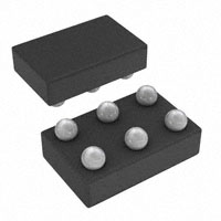
Small CSP-6 package
0.9 mm x 1.4 mm, 0.5-mm Pitch
2 A Maximum Continuous Switch Current
Low Shutdown Current
Low Threshold Control Input
Controlled Slew Rate to Avoid Inrush Currents
Quick Output Discharge Transistor
ESD Performance Tested Per JESD 22
– 5000-V Human-Body Model
(A114-B, Class II)
– 1000-V Charged-Device Model (C101)
A 1250 Ω on-chip load resistor is added for output
quick discharge when the switch is turned off. The
rise time of the device is internally controlled to avoid
inrush current. The TPS22924B features a rise time
of 100 µs at VIN = 3.6 V while the TPS22924C has a
rise time of 800 µs at VIN = 3.6 V.
The TPS22924x is available in an ultra-small spacesaving 6-pin CSP package and is characterized for
operation over the free-air temperature range of
–40ºC to 85ºC.
Device Information
PART NUMBER
PACKAGE
(1)
BODY SIZE (NOM)
TPS22924B
DSBGA (6)
1.40 mm × 0.90 mm
2 Applications
TPS22924C
DSBGA (6)
1.40 mm × 0.90 mm
•
•
•
•
•
•
•
•
•
(1) For all available packages, see the orderable addendum at
the end of the datasheet.
Battery Powered Equipment
Portable Industrial Equipment
Portable Medical Equipment
Portable Media Players
Point Of Sales Terminal
GPS Devices
Digital Cameras
Notebooks / Tablet PCs / eReaders
Smartphones
Simplified Schematic
NOTE: SMPS = Switched-mode power supply
1
An IMPORTANT NOTICE at the end of this data sheet addresses availability, warranty, changes, use in safety-critical applications,
intellectual property matters and other important disclaimers. PRODUCTION DATA.
�TPS22924B, TPS22924C
SLVSAR3E – APRIL 2011 – REVISED DECEMBER 2015
www.ti.com
Table of Contents
1
2
3
4
5
6
7
Features ..................................................................
Applications ...........................................................
Description .............................................................
Revision History.....................................................
Device Comparison Table.....................................
Pin Configuration and Functions .........................
Specifications.........................................................
7.1
7.2
7.3
7.4
7.5
7.6
7.7
7.8
7.9
7.10
8
9
1
1
1
2
3
3
4
Absolute Maximum Ratings ..................................... 4
ESD Ratings.............................................................. 4
Recommended Operating Conditions....................... 4
Thermal Information .................................................. 4
Electrical Characteristics........................................... 5
Switching Characteristics, VIN = 3.6 V ...................... 5
Switching Characteristics, VIN = 0.9 V ...................... 5
Typical Characteristics .............................................. 6
AC Characteristics (TPS22924B) ............................. 7
AC Characteristics (TPS22924C) ......................... 10
Parameter Measurement Information ................ 13
Detailed Description ............................................ 14
9.1
9.2
9.3
9.4
Overview .................................................................
Functional Block Diagram .......................................
Feature Description.................................................
Device Functional Modes........................................
14
14
14
15
10 Application and Implementation........................ 16
10.1 Application Information.......................................... 16
10.2 Typical Application ................................................ 16
11 Power Supply Recommendations ..................... 18
12 Layout................................................................... 18
12.1 Layout Guidelines ................................................. 18
12.2 Layout Example .................................................... 18
13 Device and Documentation Support ................. 19
13.1
13.2
13.3
13.4
13.5
Related Links ........................................................
Community Resources..........................................
Trademarks ...........................................................
Electrostatic Discharge Caution ............................
Glossary ................................................................
19
19
19
19
19
14 Mechanical, Packaging, and Orderable
Information ........................................................... 19
4 Revision History
NOTE: Page numbers for previous revisions may differ from page numbers in the current version.
Changes from Revision D (August 2014) to Revision E
Page
•
Added device TPS22924C .................................................................................................................................................... 1
•
Deleted Features: rON = 18.5 mΩ at VIN = 2.5 V..................................................................................................................... 1
•
Deleted Features: rON = 20.3 mΩ at VIN = 1.0 V..................................................................................................................... 1
•
Added text to the Description "while the TPS22924C has a rise time of 800 µs at VIN = 3.6 V. " ......................................... 1
•
Added: TPS22924CYZPR and TPS22924CYZPRB information to Device Comparison Table ............................................ 3
•
Added "Storage temperature" to the Absolute Maximum Ratings
•
Changed Handling Ratings to ESD Ratings........................................................................................................................... 4
•
Added section AC Characteristics (TPS22924C) ................................................................................................................ 10
•
Changed the Application Curve section ............................................................................................................................... 17
(1)
table ............................................................................ 4
Changes from Revision C (July 2014) to Revision D
•
Page
Added Pin Configuration and Functions section, Overview section, Feature Description section, Power Supply
Recommendations section .................................................................................................................................................... 1
Changes from Revision B (June 2013) to Revision C
Page
•
Added Device Information table. ............................................................................................................................................ 1
•
Added Handling Ratings table. ............................................................................................................................................... 4
•
Added Detailed Description section. .................................................................................................................................... 14
2
Submit Documentation Feedback
Copyright © 2011–2015, Texas Instruments Incorporated
Product Folder Links: TPS22924B TPS22924C
�TPS22924B, TPS22924C
www.ti.com
SLVSAR3E – APRIL 2011 – REVISED DECEMBER 2015
5 Device Comparison Table
TA
(1)
(2)
(3)
PACKAGE
(1)
ORDERABLE PART
NUMBER
TOP-SIDE MARKING
(2)
BACKSIDE
COATING (3)
RISE TIME AT
VIN = 3.3V (TYP.)
–40°C to
85°C
YZ (0.4mm height)
TPS22924BYZR
_ _ _ 5N _
No
96µs
–40°C to
85°C
YZP (0.5mm height)
TPS22924BYZPRB
_ _ _ 5N _
Yes
96µs
–40°C to
85°C
YZZ (0.35mm height)
TPS22924BYZZR
_ _ _ 7A _
No
96µs
–40°C to
85°C
YZP (0.5mm height)
TPS22924CYZPR
_ _ _ 5L _
No
800µs
–40°C to
85°C
YZP (0.4mm height)
TPS22924CYZPRB
_ _ _ 5L _
Yes
800µs
Package drawings, thermal data, and symbolization are available at www.ti.com/packaging.
The actual top-side marking has three preceding characters to denote year, month, and sequence code, and one following character to
designate the wafer fab/assembly site. Pin 1 identifier indicates solder-bump composition (1 = SnPb, • = Pb-free).
CSP (DSBGA) devices manufactured with backside coating have an increased resistance to cracking due to the increased physical
strength of the package. Devices with backside coating are highly encouraged for new designs.
6 Pin Configuration and Functions
YZ/YZP/YZZ PACKAGE
C
C
B
B
A
A
2 1
Laser Marking View
1 2
Bump View
Table 1. Pin Assignments (YZ/YZP/YZZ Package)
C
GND
ON
B
VOUT
VIN
A
VOUT
VIN
1
2
Pin Functions
NO.
NAME
DESCRIPTION
C1
GND
Ground
C2
ON
Switch control input, active high. Do not leave floating
A1, B1
VOUT
Switch output
A2, B2
VIN
Switch input, bypass this input with a ceramic capacitor to ground
Copyright © 2011–2015, Texas Instruments Incorporated
Product Folder Links: TPS22924B TPS22924C
Submit Documentation Feedback
3
�TPS22924B, TPS22924C
SLVSAR3E – APRIL 2011 – REVISED DECEMBER 2015
www.ti.com
7 Specifications
7.1 Absolute Maximum Ratings
(1)
MIN
MAX
–0.3
4
V
VIN + 0.3
V
4
V
Maximum continuous switch current, TA = –40°C to 85°C
2
A
Maximum pulsed switch current, 100-µs pulse, 2% duty cycle, TA = –40°C to 85°C
4
A
–40
85
°C
–65
150
°C
VIN
Input voltage range
VOUT
Output voltage range
VON
Input voltage range
IMAX
IPLS
TA
Operating free-air temperature range
Tstg
Storage temperature
(1)
–0.3
UNIT
Stresses beyond those listed under Absolute Maximum Ratings may cause permanent damage to the device. These are stress ratings
only, and functional operation of the device at these or any other conditions beyond those indicated under Recommended Operating
Conditions is not implied. Exposure to absolute-maximum-rated conditions for extended periods may affect device reliability.
7.2 ESD Ratings
VALUE
±5000
Charged device model (CDM), per JEDEC specification JESD22-C101,
all pins (2)
±1000
Human body model (HBM), per ANSI/ESDA/JEDEC JS-001, all pins
V(ESD)
(1)
(2)
Electrostatic discharge
UNIT
(1)
V
JEDEC document JEP155 states that 500-V HBM allows safe manufacturing with a standard ESD control process.
JEDEC document JEP157 states that 250-V CDM allows safe manufacturing with a standard ESD control process.
7.3 Recommended Operating Conditions
VIN
Input voltage
VOUT
Output voltage
VIH
High-level input voltage, ON
VIL
Low-level input voltage, ON
CIN
Input capacitance
(1)
MIN
MAX
0.75
3.6
V
VIN
V
VIN = 2.5 V to 3.6 V
1.2
3.6
VIN = 0.75 V to 2.5 V
0.9
3.6
VIN = 2.5 V to 3.6 V
0.6
VIN = 0.75 V to 2.49 V
0.4
1
(1)
UNIT
V
V
μF
See the Input Capacitor section in Application Information.
7.4 Thermal Information
TPS22924x
THERMAL METRIC
(1)
YZ/YZZ/YZP
UNIT
6 PINS
RθJA
Junction-to-ambient thermal resistance
123
RθJC(top)
Junction-to-case (top) thermal resistance
17.6
RθJB
Junction-to-board thermal resistance
22.8
ψJT
Junction-to-top characterization parameter
5.7
ψJB
Junction-to-board characterization parameter
22.6
RθJC(bot)
Junction-to-case (bottom) thermal resistance
N/A
(1)
4
°C/W
For more information about traditional and new thermal metrics, see the IC Package Thermal Metrics application report, SPRA953.
Submit Documentation Feedback
Copyright © 2011–2015, Texas Instruments Incorporated
Product Folder Links: TPS22924B TPS22924C
�TPS22924B, TPS22924C
www.ti.com
SLVSAR3E – APRIL 2011 – REVISED DECEMBER 2015
7.5 Electrical Characteristics
VIN = 0.75 V to 3.6 V (unless otherwise noted)
PARAMETER
IIN
Quiescent current
IIN(LEAK)
TEST CONDITIONS
IOUT = 0, VIN = VON
42
70
VIN = 1.8 V
50
350
95
200
VIN = 1.0 V
65
110
VIN = 0.75 V
35
70
18.3
19.7
VIN = 1.2 V
Full
Full
VIN = 1.8 V
IOUT = –200 mA
VIN = 1.2 V
VIN = 1.0 V
VIN = 0.75 V
RPD
Output pulldown
resistance (2)
VIN = 3.3 V, VON = 0, IOUT = 3 mA
ION
ON-state input leakage
current
VON = 0.9 V to 3.6 V or GND
25°C
19.4
21.8
mΩ
21.8
28.0
20.3
Full
25°C
19.5
27.4
Full
25°C
µA
25.8
19.6
Full
25°C
µA
26.0
18.5
Full
25°C
160
3.5
Full
25°C
UNIT
(1)
75
VIN = 2.5 V
(1)
(2)
TYP MAX
VIN = 2.5 V
OFF-state supply current VON = GND, OUT = 0V
ON-state resistance
MIN
VIN = 3.6 V
VIN = 3.6 V
RON
TA
21.2
28.6
22.7
25.3
Full
34.8
25°C
1250 1500
Ω
Full
0.1
µA
Typical values are at VIN = 3.3 V and TA = 25°C.
See Output Pulldown in the Application and Implementation section.
7.6 Switching Characteristics, VIN = 3.6 V
VIN = 3.6 V, TA = 25°C (unless otherwise noted)
PARAMETER
TEST CONDITIONS
TPS22924B
(TYP)
TPS22924C
(TYP)
UNIT
tON
Turn-ON time
RL = 10 Ω, CL = 0.1 μF, VIN = 3.6V
111
800
μs
tOFF
Turn-OFF time
RL = 10 Ω, CL = 0.1 μF, VIN = 3.6V
3
3
μs
tr
VOUT rise time
RL = 10 Ω, CL = 0.1 μF, VIN = 3.6V
96
800
μs
tf
VOUT fall time
RL = 10 Ω, CL = 0.1 μF, VIN = 3.6V
2.5
2.5
μs
TPS22924B
(TYP)
TPS22924C
(TYP)
UNIT
865
μs
7.7 Switching Characteristics, VIN = 0.9 V
VIN = 0.9 V, TA = 25°C (unless otherwise noted)
PARAMETER
TEST CONDITIONS
tON
Turn-ON time
RL = 10 Ω, CL = 0.1 μF, VIN = 0.9V
160
tOFF
Turn-OFF time
RL = 10 Ω, CL = 0.1 μF, VIN = 0.9V
20
20
μs
tr
VOUT rise time
RL = 10 Ω, CL = 0.1 μF, VIN = 0.9V
81
500
μs
tf
VOUT fall time
RL = 10 Ω, CL = 0.1 μF, VIN = 0.9V
5
5
μs
Copyright © 2011–2015, Texas Instruments Incorporated
Product Folder Links: TPS22924B TPS22924C
Submit Documentation Feedback
5
�TPS22924B, TPS22924C
SLVSAR3E – APRIL 2011 – REVISED DECEMBER 2015
www.ti.com
7.8 Typical Characteristics
Figure 1. On-State Resistance vs Input Voltage
Figure 2. On-State Resistance vs Temperature
Figure 3. Input Current, Quiescent vs Input Voltage
Figure 4. Input Current, Leak vs Input Voltage
Figure 5. On Input Threshold
6
Submit Documentation Feedback
Copyright © 2011–2015, Texas Instruments Incorporated
Product Folder Links: TPS22924B TPS22924C
�TPS22924B, TPS22924C
www.ti.com
SLVSAR3E – APRIL 2011 – REVISED DECEMBER 2015
7.9 AC Characteristics (TPS22924B)
VIN = 3.6 V, CL = 0.1 µF, RL = 10 Ω
VIN = 3.6 V, CL = 0.1 µF, RL = 10 Ω
Figure 7. Turn-Off Time vs Temperature
Figure 6. Turn-On Time vs Temperature
VIN = 3.6 V, CL = 0.1 µF, RL = 10 Ω
VIN = 3.6 V, CL = 0.1 µF, RL = 10 Ω
Figure 8. Rise Time vs Temperature
VIN = 0.9 V, CL = 0.1 µF, RL = 10 Ω
Figure 9. Fall Time vs Temperature
VIN = 0.9 V, CL = 0.1 µF, RL = 10 Ω
Figure 10. Turn-On Time vs Temperature
Figure 11. Turn-Off Time vs Temperature
Copyright © 2011–2015, Texas Instruments Incorporated
Product Folder Links: TPS22924B TPS22924C
Submit Documentation Feedback
7
�TPS22924B, TPS22924C
SLVSAR3E – APRIL 2011 – REVISED DECEMBER 2015
www.ti.com
AC Characteristics (TPS22924B) (continued)
VIN = 0.9 V, CL = 0.1 µF, RL = 10 Ω
VIN = 0.9 V, CL = 0.1 µF, RL = 10 Ω
Figure 12. Rise Time vs Temperature
VON = 1.8 V, CL = 0.1 µF, RL = 10 Ω
Figure 13. Fall Time vs Temperature
VON = 1.8 V, CL = 20 µF, RL = 10 Ω
Figure 14. Rise Time vs Input Voltage
Figure 15. Rise Time vs Input Voltage
CIN = 1 µF, CL = 0.1 µF, RL = 10 Ω, VIN = 0.9 V, TA = 25°C
CIN = 1 µF, CL = 0.1 µF, RL = 10 Ω, VIN = 0.9 V, TA = 25°C
Figure 17. Turn-Off Response
Figure 16. Turn-On Response
8
Submit Documentation Feedback
Copyright © 2011–2015, Texas Instruments Incorporated
Product Folder Links: TPS22924B TPS22924C
�TPS22924B, TPS22924C
www.ti.com
SLVSAR3E – APRIL 2011 – REVISED DECEMBER 2015
AC Characteristics (TPS22924B) (continued)
CIN = 47 µF, CL = 20 µF, RL = 10 Ω, VIN = 0.9 V, TA = 25°C
CIN = 47 µF, CL = 20 µF, RL = 10 Ω, VIN = 0.9 V, TA = 25°C
Figure 18. Turn-On Response
Figure 19. Turn-Off Response
CIN = 1 µF, CL = 0.1 µF, RL = 10 Ω, VIN = 3.6 V, TA = 25°C
CIN = 1 µF, CL = 0.1 µF, RL = 10 Ω, VIN = 3.6 V, TA = 25°C
Figure 20. Turn-On Response
Figure 21. Turn-Off Response
CIN = 47 µF, CL = 20 µF, RL = 10 Ω, VIN = 3.6 V, TA = 25°C
Figure 22. Turn-On Response
CIN = 47 µF, CL = 20 µF, RL = 10 Ω, VIN = 3.6 V, TA = 25°C
Figure 23. Turn-Off Response
Copyright © 2011–2015, Texas Instruments Incorporated
Product Folder Links: TPS22924B TPS22924C
Submit Documentation Feedback
9
�TPS22924B, TPS22924C
SLVSAR3E – APRIL 2011 – REVISED DECEMBER 2015
www.ti.com
7.10 AC Characteristics (TPS22924C)
3.1
1200
3.05
1000
3
800
tOFF (µs)
tON (µs)
2.95
600
2.9
2.85
400
2.8
200
2.75
0
-40
-15
10
35
60
2.7
-40
85
-15
10
35
60
85
Tem perature (°C)
Tem perature (°C)
VIN = 3.6 V, CL = 0.1 µF, RL = 10 Ω
VIN = 3.6 V, CL = 0.1 µF, RL = 10 Ω
Figure 25. Turn-Off Time vs Temperature
1000
2.4
900
2.38
800
2.36
700
2.34
600
2.32
tF (µs)
tR (µs)
Figure 24. Turn-On Time vs Temperature
500
2.3
400
2.28
300
2.26
200
2.24
100
2.22
0
-40
-15
10
35
60
2.2
-40
85
-15
Tem perature (°C)
10
35
60
85
Tem perature (°C)
VIN = 3.6 V, CL = 0.1 µF, RL = 10 Ω
VIN = 3.6 V, CL = 0.1 µF, RL = 10 Ω
Figure 26. Rise Time vs Temperature
Figure 27. Fall Time vs Temperature
1400
20
18
1200
16
14
12
800
tOFF (µs)
tON (µs)
1000
600
10
8
6
400
4
200
2
0
-40
-15
10
35
60
85
0
-40
-15
Tem perature (°C)
VIN = 0.9 V, CL = 0.1 µF, RL = 10 Ω
Submit Documentation Feedback
35
60
85
VIN = 0.9 V, CL = 0.1 µF, RL = 10 Ω
Figure 28. Turn-On Time vs Temperature
10
10
Tem perature (°C)
Figure 29. Turn-Off Time vs Temperature
Copyright © 2011–2015, Texas Instruments Incorporated
Product Folder Links: TPS22924B TPS22924C
�TPS22924B, TPS22924C
www.ti.com
SLVSAR3E – APRIL 2011 – REVISED DECEMBER 2015
AC Characteristics (TPS22924C) (continued)
700
6
600
5
500
tF (µs)
tR (µs)
4
400
3
300
2
200
1
100
0
-40
-15
10
35
60
0
-40
85
-15
10
Tem perature (°C)
35
60
85
Tem perature (°C)
VIN = 0.9 V, CL = 0.1 µF, RL = 10 Ω
VIN = 0.9 V, CL = 0.1 µF, RL = 10 Ω
Figure 30. Rise Time vs Temperature
Figure 31. Fall Time vs Temperature
1400
1200
TA = -40°C
TA = -40°C
1200
TA = 25°C
1000
TA = 25°C
TA = 85°C
TA = 85°C
1000
tR (µs)
tR (µs)
800
800
600
600
400
400
200
200
0
0
0
0.5
1
1.5
2
2.5
3
3.5
4
0
0.5
V IN (V)
1
1.5
2
2.5
3
3.5
4
V IN (V)
VON = 1.8 V, CL = 0.1 µF, RL = 10 Ω
VON = 1.8 V, CL = 20 µF, RL = 10 Ω
Figure 32. Rise Time vs Input Voltage
Figure 33. Rise Time vs Input Voltage
CIN = 1 µF, CL = 0.1 µF, RL = 10 Ω, VIN = 0.9 V, TA = 25°C
CIN = 1 µF, CL = 0.1 µF, RL = 10 Ω, VIN = 0.9 V, TA = 25°C
Figure 35. Turn-Off Response
Figure 34. Turn-On Response
Copyright © 2011–2015, Texas Instruments Incorporated
Product Folder Links: TPS22924B TPS22924C
Submit Documentation Feedback
11
�TPS22924B, TPS22924C
SLVSAR3E – APRIL 2011 – REVISED DECEMBER 2015
www.ti.com
AC Characteristics (TPS22924C) (continued)
CIN = 47 µF, CL = 20 µF, RL = 10 Ω, VIN = 0.9 V, TA = 25°C
CIN = 47 µF, CL = 20 µF, RL = 10 Ω, VIN = 0.9 V, TA = 25°C
Figure 36. Turn-On Response
Figure 37. Turn-Off Response
CIN = 1 µF, CL = 0.1 µF, RL = 10 Ω, VIN = 3.6 V, TA = 25°C
CIN = 1 µF, CL = 0.1 µF, RL = 10 Ω, VIN = 3.6 V, TA = 25°C
Figure 38. Turn-On Response
Figure 39. Turn-Off Response
CIN = 47 µF, CL = 20 µF, RL = 10 Ω, VIN = 3.6 V, TA = 25°C
Figure 40. Turn-On Response
12
Submit Documentation Feedback
CIN = 47 µF, CL = 20 µF, RL = 10 Ω, VIN = 3.6 V, TA = 25°C
Figure 41. Turn-Off Response
Copyright © 2011–2015, Texas Instruments Incorporated
Product Folder Links: TPS22924B TPS22924C
�TPS22924B, TPS22924C
www.ti.com
SLVSAR3E – APRIL 2011 – REVISED DECEMBER 2015
8 Parameter Measurement Information
Figure 42. Test Circuit and tON/tOFF Waveforms
Copyright © 2011–2015, Texas Instruments Incorporated
Product Folder Links: TPS22924B TPS22924C
Submit Documentation Feedback
13
�TPS22924B, TPS22924C
SLVSAR3E – APRIL 2011 – REVISED DECEMBER 2015
www.ti.com
9 Detailed Description
9.1 Overview
The TPS22924x is a single channel, 2-A load switch in a small, space-saving CSP-6 package. This device
implements a low resistance N-channel MOSFET with a controlled rise time for applications that need to limit the
inrush current.
This device is also designed to have very low leakage current during off state. This prevents downstream circuits
from pulling high standby current from the supply. Integrated control logic, driver, power supply, and output
discharge FET eliminates the need for additional external components, which reduces solution size and bill of
materials (BOM) count.
9.2 Functional Block Diagram
VIN
Charge
Pump
ON
Control
Logic
VOUT
GND
9.3 Feature Description
9.3.1 ON/OFF Control
The ON pin controls the state of the switch. Asserting ON high enables the switch. ON is active high and has a
low threshold, making it capable of interfacing with low-voltage signals. The ON pin is compatible with standard
GPIO logic threshold. It can be used with any microcontroller with 1.2-V, 1.8-V, 2.5-V or 3.3-V GPIOs.
9.3.2 Output Capacitor
Due to the integral body diode in the NMOS switch, a CIN greater than CL is highly recommended. A CL greater
than CIN can cause VOUT to exceed VIN when the system supply is removed. This could result in current flow
through the body diode from VOUT to VIN. A CIN to CL ratio of 10 to 1 is recommended for minimizing VIN dip
caused by inrush currents during startup.
9.3.3 Output Pulldown
The output pulldown is active when the user is turning off the main pass FET. The pulldown discharges the
output rail to approximately 10% of the rail, then the output pulldown is automatically disconnected to optimize
the shutdown current.
14
Submit Documentation Feedback
Copyright © 2011–2015, Texas Instruments Incorporated
Product Folder Links: TPS22924B TPS22924C
�TPS22924B, TPS22924C
www.ti.com
SLVSAR3E – APRIL 2011 – REVISED DECEMBER 2015
9.4 Device Functional Modes
(1)
ON (CONTROL SIGNAL)
VIN to VOUT
VOUT to GND
L
OFF
ON
H
ON
OFF
(1)
See application section Output Pulldown .
Copyright © 2011–2015, Texas Instruments Incorporated
Product Folder Links: TPS22924B TPS22924C
Submit Documentation Feedback
15
�TPS22924B, TPS22924C
SLVSAR3E – APRIL 2011 – REVISED DECEMBER 2015
www.ti.com
10 Application and Implementation
NOTE
Information in the following applications sections is not part of the TI component
specification, and TI does not warrant its accuracy or completeness. TI’s customers are
responsible for determining suitability of components for their purposes. Customers should
validate and test their design implementation to confirm system functionality.
10.1 Application Information
10.1.1 VIN to VOUT Voltage Drop
The VIN to VOUT voltage drop in the device is determined by the RON of the device and the load current. The
RON of the device depends upon the VIN condition of the device. Refer to the RON specification of the device in
the Electrical Characteristics table of this datasheet. Once the RON of the device is determined based upon the
VIN conditions, use Equation 1 to calculate the VIN to VOUT voltage drop:
ΔV = ILOAD × RON
where
•
•
•
•
ΔV = Voltage drop from VIN to VOUT
ILOAD = Load current
RON = On-resistance of the device for a specific VIN
An appropriate ILOAD must be chosen such that the IMAX specification of the device is not violated.
(1)
10.1.2 Input Capacitor
To limit the voltage drop on the input supply caused by transient inrush currents, when the switch turns on into a
discharged load capacitor or short-circuit, a capacitor needs to be placed between VIN and GND. A 1-μF ceramic
capacitor, CIN, placed close to the pins is usually sufficient. Higher values of CIN can be used to further reduce
the voltage drop.
10.1.3 Output Capacitor
A CIN to CL ratio of 10 to 1 is recommended for minimizing VIN dip caused by inrush currents during startup.
10.2 Typical Application
Figure 43. Typical Application
10.2.1 Design Requirements
DESIGN PARAMETER
EXAMPLE VALUE
VIN
3.6 V
CL
1 µF
Maximum Acceptable Inrush Current
40 mA
16
Submit Documentation Feedback
Copyright © 2011–2015, Texas Instruments Incorporated
Product Folder Links: TPS22924B TPS22924C
�TPS22924B, TPS22924C
www.ti.com
SLVSAR3E – APRIL 2011 – REVISED DECEMBER 2015
10.2.2 Detailed Design Procedure
10.2.2.1 Managing Inrush Current
When the switch is enabled, the output capacitors must be charged up from 0-V to VIN. This charge arrives in the
form of inrush current. Inrush current can be calculated using the following equation:
dv
Inrush Current = C ´
dt
where
•
C = Output capacitance
•
dv
dt = Output slew rate
(2)
The TPS22924B offers a very slow controlled rise time for minimizing inrush current. This device can be selected
based upon the maximum acceptable slew rate which can be calculated using the design requirements and the
inrush current equation. An output capacitance of 1.0 μF will be used since the amount of inrush increases with
output capacitance:
dv
40 mA = 1.0 mF ´
dt
(3)
dv
= 40 V/ms
dt
(4)
To ensure an inrush current of less than 40 mA, a device with a slew rate less than 40 V/ms must be used.
The TPS22924B has a typical rise time of 96 μs at 3.6 V. This results in a slew rate of 37.5 V/ms which meets
the above design requirements. For an even lower inrush current requirement, the TPS22924C can be used. The
slower rise time of 800 μs at 3.6V results in a slew rate of 4.5 V/ms, well below the design requirements.
10.2.3 Application Curve
VIN = 3.6 V
CL = 1 µF
TA = 25°C
Figure 44. TPS22924B Inrush Current With a 1 µF
Capacitor
VIN = 3.6 V
CL = 1 µF
TA = 25°C
Figure 45. TPS22924C Inrush Current With a 1 µF
Capacitor
Copyright © 2011–2015, Texas Instruments Incorporated
Product Folder Links: TPS22924B TPS22924C
Submit Documentation Feedback
17
�TPS22924B, TPS22924C
SLVSAR3E – APRIL 2011 – REVISED DECEMBER 2015
www.ti.com
11 Power Supply Recommendations
The device is designed to operate with a VIN range of 0.75 V to 3.6 V. This supply must be well regulated and
placed as close to the device terminal as possible with the recommended 1 µF bypass capacitor. If the supply is
located more than a few inches from the device terminals, additional bulk capacitance may be required in
addition to the ceramic bypass capacitors. If additional bulk capacitance is required, an electrolytic, tantalum, or
ceramic capacitor of 10 µF may be sufficient.
12 Layout
12.1 Layout Guidelines
For best performance, all traces should be as short as possible. To be most effective, the input and output
capacitors should be placed close to the device to minimize the effects that parasitic trace inductances may have
on normal and short-circuit operation. Using wide traces for VIN, VOUT, and GND helps minimize the parasitic
electrical effects.
12.2 Layout Example
Figure 46. TPS22924x Layout Example
18
Submit Documentation Feedback
Copyright © 2011–2015, Texas Instruments Incorporated
Product Folder Links: TPS22924B TPS22924C
�TPS22924B, TPS22924C
www.ti.com
SLVSAR3E – APRIL 2011 – REVISED DECEMBER 2015
13 Device and Documentation Support
13.1 Related Links
The table below lists quick access links. Categories include technical documents, support and community
resources, tools and software, and quick access to sample or buy.
Table 2. Related Links
PARTS
PRODUCT FOLDER
SAMPLE & BUY
TECHNICAL
DOCUMENTS
TOOLS &
SOFTWARE
SUPPORT &
COMMUNITY
TPS22924B
Click here
Click here
Click here
Click here
Click here
TPS22924C
Click here
Click here
Click here
Click here
Click here
13.2 Community Resources
The following links connect to TI community resources. Linked contents are provided "AS IS" by the respective
contributors. They do not constitute TI specifications and do not necessarily reflect TI's views; see TI's Terms of
Use.
TI E2E™ Online Community TI's Engineer-to-Engineer (E2E) Community. Created to foster collaboration
among engineers. At e2e.ti.com, you can ask questions, share knowledge, explore ideas and help
solve problems with fellow engineers.
Design Support TI's Design Support Quickly find helpful E2E forums along with design support tools and
contact information for technical support.
13.3 Trademarks
E2E is a trademark of Texas Instruments.
All other trademarks are the property of their respective owners.
13.4 Electrostatic Discharge Caution
These devices have limited built-in ESD protection. The leads should be shorted together or the device placed in conductive foam
during storage or handling to prevent electrostatic damage to the MOS gates.
13.5 Glossary
SLYZ022 — TI Glossary.
This glossary lists and explains terms, acronyms, and definitions.
14 Mechanical, Packaging, and Orderable Information
The following pages include mechanical, packaging, and orderable information. This information is the most
current data available for the designated devices. This data is subject to change without notice and revision of
this document. For browser-based versions of this data sheet, refer to the left-hand navigation.
Copyright © 2011–2015, Texas Instruments Incorporated
Product Folder Links: TPS22924B TPS22924C
Submit Documentation Feedback
19
�PACKAGE OPTION ADDENDUM
www.ti.com
10-Dec-2020
PACKAGING INFORMATION
Orderable Device
Status
(1)
Package Type Package Pins Package
Drawing
Qty
Eco Plan
(2)
Lead finish/
Ball material
MSL Peak Temp
Op Temp (°C)
Device Marking
(3)
(4/5)
(6)
TPS22924BYZPRB
ACTIVE
DSBGA
YZP
6
3000
RoHS & Green
SNAGCU
Level-1-260C-UNLIM
-40 to 85
5N
TPS22924BYZR
ACTIVE
DSBGA
YZ
6
3000
RoHS & Green
SNAGCU
Level-1-260C-UNLIM
-40 to 85
5N
TPS22924BYZT
ACTIVE
DSBGA
YZ
6
250
RoHS & Green
SNAGCU
Level-1-260C-UNLIM
-40 to 85
5N
TPS22924BYZZR
ACTIVE
DSBGA
YZZ
6
3000
RoHS & Green
SNAGCU
Level-1-260C-UNLIM
-40 to 85
7A
TPS22924BYZZT
ACTIVE
DSBGA
YZZ
6
250
RoHS & Green
SNAGCU
Level-1-260C-UNLIM
-40 to 85
7A
TPS22924CYZPR
ACTIVE
DSBGA
YZP
6
3000
RoHS & Green
SNAGCU
Level-1-260C-UNLIM
-40 to 85
(5L, 5LG)
TPS22924CYZPRB
ACTIVE
DSBGA
YZP
6
3000
RoHS & Green
SNAGCU
Level-1-260C-UNLIM
-40 to 85
5L
TPS22924CYZPT
ACTIVE
DSBGA
YZP
6
250
RoHS & Green
SNAGCU
Level-1-260C-UNLIM
-40 to 85
(5LF, 5LG)
(1)
The marketing status values are defined as follows:
ACTIVE: Product device recommended for new designs.
LIFEBUY: TI has announced that the device will be discontinued, and a lifetime-buy period is in effect.
NRND: Not recommended for new designs. Device is in production to support existing customers, but TI does not recommend using this part in a new design.
PREVIEW: Device has been announced but is not in production. Samples may or may not be available.
OBSOLETE: TI has discontinued the production of the device.
(2)
RoHS: TI defines "RoHS" to mean semiconductor products that are compliant with the current EU RoHS requirements for all 10 RoHS substances, including the requirement that RoHS substance
do not exceed 0.1% by weight in homogeneous materials. Where designed to be soldered at high temperatures, "RoHS" products are suitable for use in specified lead-free processes. TI may
reference these types of products as "Pb-Free".
RoHS Exempt: TI defines "RoHS Exempt" to mean products that contain lead but are compliant with EU RoHS pursuant to a specific EU RoHS exemption.
Green: TI defines "Green" to mean the content of Chlorine (Cl) and Bromine (Br) based flame retardants meet JS709B low halogen requirements of