Product
Folder
Sample &
Buy
Support &
Community
Tools &
Software
Technical
Documents
TPS22946
SLVS984B – SEPTEMBER 2009 – REVISED MARCH 2015
TPS22946 Ultralow Power, Low Input Voltage, Current-Limited Load Switch
With Shutoff, Auto-Restart, and Overcurrent Condition Time-Out
1 Features
•
1
•
•
•
•
•
•
•
•
•
•
•
•
Ultralow Quiescent Current 1 μA (Typical)
at VIN = 1.8 V
Input Voltage Range: 1.62 V to 5.5 V
Low ON-Resistance
– rON = 300 mΩ at VIN = 5.5 V
– rON = 400 mΩ at VIN = 3.3 V
– rON = 500 mΩ at VIN = 2.5 V
– rON = 600 mΩ at VIN = 1.8 V
Selectable Minimum Current Limit:
155 mA, 70 mA, or 30 mA
Integrated Inrush Current Time-out (8 ms)
Shutdown Current: < 1 μA
Thermal Shutdown
Fault Blanking
Auto Restart
Overcurrent Condition Time-out (Automatic
Disable for Permanent Overcurrent)
1.8-V Compatible Control Input
ESD Performance Tested Per JESD 22
– 6000-V Human-Body Model
(A114-B, Class II)
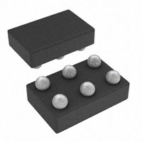
Tiny DSGBA Package 1.4 mm × 0.9 mm (YZP)
2 Applications
•
•
•
•
•
•
Fingerprint Module Protection
Portable Consumer Electronics
Mobile Phones
Smartphones
Notebooks
GPS Devices
When the switch current reaches the maximum limit,
the TPS22946 operates in a constant-current mode to
prohibit excessive currents from causing damage.
The current limit can be selected using the CL input:
a high CL input sets the current limit to 155 mA, a low
CL input sets the current limit to 70 mA, and a
floating CL input sets the current limit to 30 mA.
If the constant current condition persists after 10 ms,
the switch is turned off and the fault signal pin (OC) is
pulled low. The TPS22946 has an auto-restart feature
which turns the switch on again after 70 ms if the ON
pin is still active. If the TPS22946 remains in an overcurrent condition for 5 seconds, the device shuts off
until it is turned on again by setting the ON control
signal off and then on.
If the device is used to protect an LDO, the inrush
current required by the LDO at startup can, in some
cases, exceed the current limit and initiate a blanking
(current limiting) condition. The TPS22946 provides
allowance for this scenario during startup of the LDO
by temporarily increasing the current limit to 435 mA
for 8 ms after the load switch is enabled.
The TPS22946 is available in space-saving 6-pin
DSBGA (YZP) package. The device is characterized
for operation over the free-air temperature range of
–40°C to 85°C.
Device Information(1)
PART NUMBER
TPS22946
PACKAGE
BODY SIZE (NOM)
DSBGA (6)
0.90 mm × 1.40 mm
(1) For all available packages, see the orderable addendum at
the end of the data sheet.
Typical Application Schematic
Power
Supply
VIN
VOUT
CLOAD
CIN
RLOAD
3 Description
The TPS22946 is an ultralow power load switch that
provides protection to systems and loads in highcurrent conditions. The device contains a 300-mΩ
current-limited P-channel MOSFET that can operate
over an input voltage range of 1.62 V to 5.5 V. The
switch is controlled by an on/off input (ON), which can
interface directly with low-voltage control signals. The
TPS22946 includes thermal shutdown protection that
prevents damage to the device when a continuous
over-current condition causes excessive heating by
turning off the switch.
CL
GND
VDD
ON
ON
OC
OFF
1
An IMPORTANT NOTICE at the end of this data sheet addresses availability, warranty, changes, use in safety-critical applications,
intellectual property matters and other important disclaimers. PRODUCTION DATA.
�TPS22946
SLVS984B – SEPTEMBER 2009 – REVISED MARCH 2015
www.ti.com
Table of Contents
1
2
3
4
5
6
7
8
Features ..................................................................
Applications ...........................................................
Description .............................................................
Revision History.....................................................
Pin Configuration and Functions .........................
Specifications.........................................................
1
1
1
2
3
4
6.1
6.2
6.3
6.4
6.5
6.6
6.7
4
4
4
4
5
6
7
Absolute Maximum Ratings ......................................
ESD Ratings..............................................................
Recommended Operating Conditions.......................
Thermal Information ..................................................
Electrical Characteristics...........................................
Switching Characteristics ..........................................
Typical Characteristics ..............................................
Parameter Measurement Information ................ 11
Detailed Description ............................................ 12
8.1 Overview ................................................................. 12
8.2 Functional Block Diagram ....................................... 12
8.3 Feature Description................................................. 13
8.4 Device Functional Modes........................................ 21
9
Application and Implementation ........................ 25
9.1 Application Information............................................ 25
9.2 Typical Application ................................................. 25
10 Power Supply Recommendations ..................... 27
11 Layout................................................................... 27
11.1 Layout Guidelines ................................................. 27
11.2 Layout Example .................................................... 27
12 Device and Documentation Support ................. 28
12.1 Trademarks ........................................................... 28
12.2 Electrostatic Discharge Caution ............................ 28
12.3 Glossary ................................................................ 28
13 Mechanical, Packaging, and Orderable
Information ........................................................... 28
4 Revision History
Changes from Revision A (February 2010) to Revision B
•
2
Page
Added Pin Configuration and Functions section, ESD Ratings table, Feature Description section, Device Functional
Modes, Application and Implementation section, Power Supply Recommendations section, Layout section, Device
and Documentation Support section, and Mechanical, Packaging, and Orderable Information section .............................. 1
Submit Documentation Feedback
Copyright © 2009–2015, Texas Instruments Incorporated
Product Folder Links: TPS22946
�TPS22946
www.ti.com
SLVS984B – SEPTEMBER 2009 – REVISED MARCH 2015
5 Pin Configuration and Functions
6-Pin DSBGA
YZP Package
C
C
B
B
A
A
2 1
Laser Marking View
1 2
Bump View
Pin Assignments
C
ON
OC
B
CL
GND
A
VIN
VOUT
2
1
Pin Functions
PIN
I/O
DESCRIPTION
NO.
NAME
A1
VOUT
O
Output of the power switch
A2
VIN
I
Supply. Input to the power switch and the supply voltage for the device
B1
GND
–
Ground
B2
CL
I
Current limit selection. CL high is 155-mA current limit, CL low is 70-mA current limit, and CL floating is
30-mA current limit.
C1
OC
O
Overcurrent output flag. Active-low open-drain output that indicates an overcurrent, supply undervoltage,
or overtemperature state.
C2
ON
I
On/off control input
Submit Documentation Feedback
Copyright © 2009–2015, Texas Instruments Incorporated
Product Folder Links: TPS22946
3
�TPS22946
SLVS984B – SEPTEMBER 2009 – REVISED MARCH 2015
www.ti.com
6 Specifications
6.1 Absolute Maximum Ratings
over operating free-air temperature range (unless otherwise noted)
VI
Input voltage
TJ
Operating junction temperature
VIN, VOUT, ON, CL
Tstg Storage temperature
MIN
MAX
UNIT
–0.3
6
V
–40
125
°C
–65
150
°C
VALUE
UNIT
6.2 ESD Ratings
V(ESD)
(1)
(2)
Electrostatic discharge
Human body model (HBM), per JEDEC specification JESD22 (A114-B,
Class II) (1)
±6000
Charged-device model (CDM), per JEDEC specification JESD22C101 (2)
±2000
V
JEDEC document JEP155 states that 500-V HBM allows safe manufacturing with a standard ESD control process.
JEDEC document JEP157 states that 250-V CDM allows safe manufacturing with a standard ESD control process.
6.3 Recommended Operating Conditions
over operating free-air temperature range (unless otherwise noted)
VIN
Input voltage
VON
ON pin voltage
VCL
CL pin voltage
VOUT
OUT pin voltage
TA
Ambient free-air temperature
tCLSET
CL pin setting time
CIN
Input capacitor
VIH
ON high-level input voltage
MIN
MAX
1.62
5.5
UNIT
V
0
5.5
V
0
VIN
V
0
VIN
V
–40
85
°C
8
ms
1 (1)
μF
VIN = 1.8 V
1.1
5.5
VIN = 2.5 V
1.2
5.5
VIN = 3.3 V
1.3
5.5
VIN = 5.5 V
1.4
5.5
VIN = 1.8 V
0.4
VIN = 2.5 V
0.4
VIN = 3.3 V
0.5
V
VIL
ON low-level input voltage
VIH
CL low-level input voltage
VIN = 1.62 V to 5.5 V, IIH = 55 μA
0.7 VIN
VIN
V
VIL
CL high-level input voltage
VIN = 1.62 V to 5.5 V, IIL = 55 μA
GND
0.3 VIN
V
VIN = 5.5 V
(1)
V
0.6
See Application Information.
6.4 Thermal Information
TPS22946
THERMAL METRIC
(1)
YZP (DSBGA)
UNIT
6 PINS
RθJA
Junction-to-ambient thermal resistance
RθJC(top)
Junction-to-case (top) thermal resistance
1.3
RθJB
Junction-to-board thermal resistance
22.6
ψJT
Junction-to-top characterization parameter
5.2
ψJB
Junction-to-board characterization parameter
22.6
(1)
4
131
°C/W
For more information about traditional and new thermal metrics, see the IC Package Thermal Metrics application report, SPRA953.
Submit Documentation Feedback
Copyright © 2009–2015, Texas Instruments Incorporated
Product Folder Links: TPS22946
�TPS22946
www.ti.com
SLVS984B – SEPTEMBER 2009 – REVISED MARCH 2015
6.5 Electrical Characteristics
VIN = 1.62 V to 5.5 V, TYP values at TA = 25°C (unless otherwise noted)
PARAMETER
TEST CONDITIONS
IOUT = 0 mA, VIN = 4.5 V to 5.5 V
IIN
Average quiescent current
TA
(1)
MIN
Full range
IOUT = 0 mA, VIN = 3.0 V to 3.6 V
IOUT = 0 mA, VIN = 1.62 V to 1.98 V
TYP
MAX
1.5
5
1.3
4
1
3
UNIT
μA
IIN(OFF)
OFF state supply current
VON = 0 V
VIN = 3.6 V, VOUT open
Full range
0.1
1
μA
IOUT(LEAKAGE)
OFF state switch current
VON = 0 V
VIN = 3.6 V,
VOUT short to GND
Full range
0.1
1.1
μA
25°C
0.3
0.4
VIN = 5.5 V
VIN = 3.3 V
rON
ON-state resistance
IOUT = –100 mA
VIN = 2.5 V
VIN = 1.8 V
VIN = 1.62 V
ION
ON input leakage current
ILIM
Current limit
Ilimit_inrush
Inrush current limit
Full range
0.5
0.55
25°C
0.5
Full range
0.6
0.65
25°C
0.6
Full range
0.8
25°C
0.7
0.9
1
VON = VIN or GND
Full range
1
VIN = 1.8 V, VOUT = 1.5 V, CL = GND
Full range
70
85
120
VIN = 3.3 V, VOUT = 3.0 V, CL = GND
Full range
60
80
115
VIN = 1.8 V, VOUT = 1.5 V, CL = VIN
Full range
155
175
235
VIN = 3.3 V, VOUT = 3.0 V, CL = VIN
Full range
135
165
230
VIN = 1.8 V, VOUT = 1.5 V, CL floating
Full range
30
45
60
VIN = 3.3 V, VOUT = 3.0 V, CL floating
Full range
28
40
60
Rl = 1 Ω, VIN = 3.3 V, VOUT = 2.3 V
Full range
375
435
685
Return from shutdown
VIN = 5 V, ISINK = 10 mA
VOL
OC output logic low voltage
IOH
OC output high leakage current VIN = 5 V, Switch ON
VIN = 1.8 V, ISINK = 10 mA
Ω
0.85
Full range
μA
mA
mA
135
Full range
Hysteresis
(1)
(2)
0.4
Full range
Shutdown threshold
Thermal shutdown (2)
0.45
25°C
125
°C
10
Full range
Full range
0.1
0.2
0.1
0.3
1
V
μA
Full range TA = –40°C to 85°C
See Overtemperature Protection.
Submit Documentation Feedback
Copyright © 2009–2015, Texas Instruments Incorporated
Product Folder Links: TPS22946
5
�TPS22946
SLVS984B – SEPTEMBER 2009 – REVISED MARCH 2015
www.ti.com
6.6 Switching Characteristics
VIN = 1.8 V, RL = 50 Ω, CL = 1 μF, TA = –40°C to 85°C, TYP values at TA = 25°C (unless otherwise noted)
PARAMETER
TEST CONDITIONS
MIN
TYP
MAX
UNIT
tPWRON
Power-on time
RL = 50 Ω, CL = 1 μF
192
μs
tPWROFF
Power-off time
RL = 50 Ω, CL = 1 μF
0.55
μs
tON
Turnon time
RL = 50 Ω, CL = 1 μF
125
μs
tOFF
Turnoff time
RL = 50 Ω, CL = 1 μF
115
μs
tR
VOUT rise time
RL = 50 Ω, CL = 1 μF
35
μs
tF
VOUT fall time
RL = 50 Ω, CL = 1 μF
120
tBLANK
Overcurrent blanking time
tRSTART
Auto-restart time
tTIMEOUT
Overcurrent detection time-out (1)
tOVRTMP
Overtemperature detection maximum
response time
tMODOC
Moderate overcurrent detection
maximum response time
tHARDSHOR
T
(1)
(2)
(3)
6
Hard-short detection maximum
response time
7
50
VIN = VON = 3.3 V, hard short (2)
μs
10
15
ms
70
95
ms
6000
ms
7.7
ms
VIN = VON = 1.8 V, Moderate over-current
condition (3)
63.5
VIN = VON = 3.3 V, Moderate overcurrent condition (3)
65.5
VIN = VON = 1.8 V, hard short (2)
270
VIN = VON = 3.3 V, hard short (2)
295
ms
μs
See Automatic Disable in Case of Permanent Overcurrent.
Hard short check is performed at the output voltage of the switch. Hard short condition is active when VOUT < 2/3 VIN.
If the current going through the switch is above ILIM, then the moderate over-current condition is activated
Submit Documentation Feedback
Copyright © 2009–2015, Texas Instruments Incorporated
Product Folder Links: TPS22946
�TPS22946
www.ti.com
SLVS984B – SEPTEMBER 2009 – REVISED MARCH 2015
6.7 Typical Characteristics
0.8
0.8
0.7
0.7
V IN = 1.8 V
TA = 85°C
0.6
ON Resistance (Ohm)
ON Resistance (Ohm)
0.6
TA = 25°C
0.5
0.4
TA = -40°C
0.3
0.5
V IN = 3.3 V
0.4
0.3
V IN = 5.5 V
0.2
0.2
0.1
0.1
0
0
1.62
1.8
2.5
3.3
5.5
-40.00
V IN
Figure 1. ON-Resistance vs Input Voltage
Figure 2. ON-Resistance Vs Temperature
V IN = 5.5 V
500
2
V IN = 5.5 V
IIN (Leakage) (nA)
IIN (Quiescent) (µA)
85.00
600
2.5
1.5
25.00
Tem perature (°C)
V IN = 3.3 V
1
V IN = 1.8 V
400
300
200
V IN = 3.3 V
0.5
100
V IN = 1.8 V
0
-40.00
25.00
0
85.00
-40.00
25.00
85.00
Tem perature (°C)
Tem perature (°C)
Figure 3. Input Current (Quiescent) vs Temperature
Figure 4. Input Current (Leakage) vs Temperature
450
200
400
180
V IN = 5.5 V
160
350
140
300
120
ILIM (mA)
IIN (Off) (nA)
CL = High
250
200
100
CL = Low
80
150
V IN = 3.3 V
100
60
CL = Float
40
50
20
V IN = 1.8 V
0
-40.00
25.00
85.00
0
-50
Tem perature (°C)
-25
0
25
50
75
100
Tem perature (°C)
Figure 5. Input Current (Off) vs Temperature
Figure 6. Current Limit vs Temperature
Submit Documentation Feedback
Copyright © 2009–2015, Texas Instruments Incorporated
Product Folder Links: TPS22946
7
�TPS22946
SLVS984B – SEPTEMBER 2009 – REVISED MARCH 2015
www.ti.com
Typical Characteristics (continued)
200
11.4
180
CL = High
11.2
V IN = 5.5 V
160
11
V IN = 3.3 V
140
10.8
t Blank (ms)
ILIM (mA)
120
100
CL = Low
80
10.6
V IN = 1.8 V
10.4
60
10.2
CL = Float
40
10
20
0
0
1
2
3
4
5
9.8
-50
6
-25
0
25
50
75
100
Tem perature (°C)
V IN (V)
Figure 7. Current Limit vs Input Voltage
Figure 8. tBlank vs Temperature
250
80
78
200
76
t PWRON (µs)
t Restart (ms)
V IN = 5.5 V
74
V IN = 3.3 V
V IN = 1.8 V
72
150
100
70
50
68
66
-50
0
-25
0
25
50
75
-40
100
25
85
Tem perature (°C)
Tem perature (°C)
Figure 10. tPWRON vs Temperature
Figure 9. tReset vs Temperature
6
1
V IN = 5.5 V
0.9
5
0.8
4
V IN = 3.3 V
V OUT (V)
t PWROFF (µs)
0.7
0.6
3
V IN = 2.5 V
0.5
V IN = 1.8 V
2
0.4
V IN = 1.62 V
1
0.3
0.2
0
-40
25
85
0
Figure 11. tPWROFF vs Temperature
8
0.5
1
1.5
2
V ON (V)
Tem perature (°C)
Submit Documentation Feedback
Figure 12. ON Threshold
Copyright © 2009–2015, Texas Instruments Incorporated
Product Folder Links: TPS22946
�TPS22946
www.ti.com
SLVS984B – SEPTEMBER 2009 – REVISED MARCH 2015
Typical Characteristics (continued)
VON
VIN = 3.3 V
CIN = 1 µF
COUT = 0.1 µF
RL = 500 mW
IOUT
VON
IOUT
VIN = 3.3 V
CIN = 1 µF
COUT = 0.1 µF
RL = 500 mW
Figure 13. tON Response
Figure 14. tOFF Response
VDRV
(see Note)
VDRV
(see Note)
VOUT
VOUT
IOUT
IOUT
VOC
VOC
NOTE: VDRV signal forces the device to go into over-current mode.
NOTE: VDRV signal forces the device to go into over-current mode.
Figure 16. tRestart Response
Figure 15. tBlank Response
VIN
IOUT
VON
VOUT
IOUT
Input and enable pins tied together
VOUT shorted to GND
VIN = VON = 3.3 V
CIN = 10 µF
COUT = 1 µF
RL = 2 W
VIN = 3.3 V
CIN = 10 µF
COUT = 1 µF
VOUT
Figure 17. Hard Short-Circuit Response
Figure 18. Short-Circuit Response
Submit Documentation Feedback
Copyright © 2009–2015, Texas Instruments Incorporated
Product Folder Links: TPS22946
9
�TPS22946
SLVS984B – SEPTEMBER 2009 – REVISED MARCH 2015
www.ti.com
Typical Characteristics (continued)
VON
IOUT
VIN
VOUT
VIN = VON = 3.3 V
CIN = 10 µF
COUT = 1 µF
RL = 5 W
Figure 19. Moderate Overcurrent Response
10
Submit Documentation Feedback
Copyright © 2009–2015, Texas Instruments Incorporated
Product Folder Links: TPS22946
�TPS22946
www.ti.com
SLVS984B – SEPTEMBER 2009 – REVISED MARCH 2015
7 Parameter Measurement Information
VIN
ON
VOUT
(A)
TPS22946
RL
CL
+
–
OFF
CIN =1 µF
GND
GND
GND
TEST CIRCUIT
1.8 V
VON
VON
VON/2
VON/2
tr
0V
tON
tOFF
90%
VOUT
VOH
VOUT
tf
0V
VOUT/2
VOUT/2
10%
90%
10%
VOL
tON/tOFF WAVEFORMS
Figure 20. Test Circuit and tON/tOFF Waveforms
VIN
VIN
VIN/2
VIN/2
0V
0V
tPWRON
tPWROFF
VOL
VOUT
VOUT/2
VOUT/2
VOH
VON
Figure 21. tPWRON/tPWROFF Waveforms
Submit Documentation Feedback
Copyright © 2009–2015, Texas Instruments Incorporated
Product Folder Links: TPS22946
11
�TPS22946
SLVS984B – SEPTEMBER 2009 – REVISED MARCH 2015
www.ti.com
8 Detailed Description
8.1 Overview
The TPS22946 is an ultralow power load switch that provides protection to systems and loads in high-current
conditions. The device contains a 300-mΩ current-limited P-channel MOSFET that can operate over an input
voltage range of 1.62 V to 5.5 V. The switch is controlled by an on/off input (ON), which is capable of
interfacing directly with low-voltage control signals. The TPS22946 includes thermal shutdown protection that
prevents damage to the device when a continuous over-current condition causes excessive heating by
turning off the switch.
When the switch current reaches the maximum limit, the TPS22946 operates in a constant-current mode to
prohibit excessive currents from causing damage. The current limit can be selected using the CL input: a
high CL input sets the current limit to 155 mA, a low CL input sets the current limit to 70 mA, and a floating
CL input sets the current limit to 30 mA.
If the constant current condition still persists after 10 ms, the switch is turned off and the fault signal pin (OC)
is pulled low. The TPS22946 has an auto-restart feature which turns the switch on again after 70 ms if the
ON pin is still active. If the TPS22946 remains in an over-current condition for 5 seconds, the device shuts
off until it is turned on again by setting the ON control signal off and then on.
If the device is used to protect an LDO, the inrush current required by the LDO at startup can, in some
cases, exceed the current limit and initiate a blanking (current limiting) condition. The TPS22946 device
provides allowance for this scenario during startup of the LDO by temporarily increasing the current limit to
435 mA for 8 ms after the load switch is enabled.
The TPS22946 is available in a space-saving 6-pin DSBGA (YZP) package. The device is characterized for
operation over the free-air temperature range of –40°C to 85°C.
Table 1. Feature List
TPS22946
rON (TYP) AT
5.5 V
CURRENT LIMIT
INTEGRATED INRUSH
CURRENT TIME-OUT
CURRENT LIMIT
BLANKING TIME
AUTORESTART
TIME
OVERCURRENT
TIME-OUT
ENABLE
300 mΩ
30 mA, 70 mA, or
155 mA
Yes
10 ms
70 ms
6s
Active high
8.2 Functional Block Diagram
A2
VIN
B2
CL
ON
HardShort
Detection
C2
Control
Logic
Current
Limit
A1
VOUT
Thermal
Shutdown
Oscillator
C1
OC
B1
GND
12
Submit Documentation Feedback
Copyright © 2009–2015, Texas Instruments Incorporated
Product Folder Links: TPS22946
�TPS22946
www.ti.com
SLVS984B – SEPTEMBER 2009 – REVISED MARCH 2015
8.3 Feature Description
8.3.1 Detection Schemes
8.3.1.1 Overtemperature Detection
The thermal shutdown detection circuit is active every 8 ms for a period of 0.5 ms. The thermal shutdown
protects the part from internally or externally generated excessive temperatures. During an over-temperature
condition the switch is turned-off (Open). The switch automatically turns-on (closes) again if temperature of the
die drops below the threshold temperature while the part is still enabled.
In addition, if an overcurrent fault condition is detected due to a moderate overcurrent or a hard-short, the
thermal shutdown is activated immediately and stays on continuously for the duration of blanking (see Figure 32).
VIN
VIN/2
0V
VON is tied directly to VIN
VON
0V
tPWRON
VOUT/2
VOUT
140°C
129°C
Normal Temperature
Temperature (°C)
Inrush current window
Over Temperature
Detection
Load Switch Status
SWITCH
OPEN
Over Temperature
resumes the normal cycle
8mS
tOVRTMP
0.5 ms
ON
OFF
ON
Over temperature detected
during the ON cycle
OFF
SWITCH
CLOSE
0.5 ms tOVRTMP
OFF
ON
SWITCH
OPEN
ON
OFF
SWITCH
CLOSE
NOTE: Case where the temperature causes the overtemperature detection circuit to trip before the other detection schemes.
Figure 22. Overtemperature Detection
Submit Documentation Feedback
Copyright © 2009–2015, Texas Instruments Incorporated
Product Folder Links: TPS22946
13
�TPS22946
SLVS984B – SEPTEMBER 2009 – REVISED MARCH 2015
www.ti.com
Feature Description (continued)
8.3.1.2 Hard-Short Detection
The hard-short detection circuit is active every 250 μs for a period of 125 μs. A comparator monitors the output
voltage, VOUT. A hard short is detected when VOUT is lower than 2/3 VIN. The switch then goes into currentlimiting mode.
VIN
VIN/2
0V
VON is tied directly to VIN
VON
0V
A hard short occurs on
Vout
tPWRON
VOUT/2
VOUT
Current increases
through switch
proportional to VOUT
Over current due to hard
short
Current is
limited
No current.
Switch is off
IOUT
tBLANK
tRSTART
tBLANK
tRSTART
tTIMEOUT
Hard short detected during the ON cycle
0.125mS
Hard Short
Detection
OFF
OFF
ON
ON
OFF
tHARDSHORT
Inrush Current window
8 ms
tOVRTMP
Over Temperature
Detection
ON
OFF
tBLANK
Load Switch Status
SWITCH
OPEN
SWITCH
CLOSE
tRSTART
SWITCH
OPEN
tBLANK
SWITCH
CLOSE
tRSTART
SWITCH
OPEN
Figure 23. Hard-Short Detection
14
Submit Documentation Feedback
Copyright © 2009–2015, Texas Instruments Incorporated
Product Folder Links: TPS22946
�TPS22946
www.ti.com
SLVS984B – SEPTEMBER 2009 – REVISED MARCH 2015
Feature Description (continued)
8.3.1.3 Moderate Overcurrent Detection
The moderate overcurrent detection circuit is active every 64 ms for a period of 0.5 ms. A moderate over-current
condition is triggered when the output current of the switch exceeds the current limit value and is not yet into
hard short condition. The switch then goes into current-limiting mode.
VIN
0V
VIN/2
VON is tied directly to VIN
VON
0V
A moderate short
occurs on Vout
tPWRON
VOUT/2
VOUT
Current increases
through switch
proportional to VOUT
Over current
Current is
limited
No current
Switch is off
IOUT
Inrush current window
8mS
Moderate Over Current
Detection
OFF
ON
tMODOC
tBLANK
tRSTART
Inrush current window
tOVRTMP
8mS
Over Temperature
Detection
tTIMEOUT
OFF
ON
ON
tBLANK
tRSTART
0.125 ms
Hard Short
Detection
OFF
ON
OFF
ON
OFF
ON
OFF
ON
ON
OFF
ON
OFF
ON
OFF
ON
OFF
ON
tHARDSHORT
Load Switch Status
SWITCH
OPEN
SWITCH
CLOSE
SWITCH
OPEN
NOTE: The overcurrent does not cause the temperature to go above 140°C here.
Figure 24. Moderate Overcurrent Detection
Submit Documentation Feedback
Copyright © 2009–2015, Texas Instruments Incorporated
Product Folder Links: TPS22946
15
�TPS22946
SLVS984B – SEPTEMBER 2009 – REVISED MARCH 2015
www.ti.com
Feature Description (continued)
8.3.1.4 Current Limiting Mode
When an overcurrent condition (moderate or a hard short) is detected, the TPS22946 operates in a constantcurrent mode to prohibit excessive currents from causing damage. TPS22946 has a current limit of 30 mA, 70
mA, or 155 mA.
If the constant current condition still persists after 10ms, the device shuts off the switch and pulls the fault signal
pin (OC) low. The TPS22946 has an auto-restart feature which turns the switch on again after 70 ms if the ON
pin is still active.
8.3.1.5 Fault Reporting
When a moderate overcurrent, hard short or overtemperature condition is detected, OC is set active low to signal
a fault condition. OC is an open-drain MOSFET and requires a pullup resistor between VIN and OC. During
shutdown, the pulldown on OC is disabled, reducing current draw from the supply.
8.3.1.6 Power-On and Power-Off Sequence
The device is enabled internally only once the hard-short detection circuit is enabled.
16
Submit Documentation Feedback
Copyright © 2009–2015, Texas Instruments Incorporated
Product Folder Links: TPS22946
�TPS22946
www.ti.com
SLVS984B – SEPTEMBER 2009 – REVISED MARCH 2015
Feature Description (continued)
VIN
VIN/2
VON is tied directly to VIN
0V
VON
tPWRON
0V
LDO Output stable
Allotted time for LDO Inrush Current to
exceed normal current limit threshold
VOUT
Temporarily increase current limit threshold to
allow for LDO Inrush current
Current Limit as set by CL
(30 mA, 70 mA, 155 mA)
ILIMIT_INRUSH
tPWRON
Current Limit
Threshold
8 ms
Changes on CL pin, will not affect current
limit threshold after this time
CL pin
Detection
Timing
tCLSET
Inrush Current window
Moderate Over
Current Detection
tMODOC
8 ms
0.5ms
tMODOC
Inrush Current window
Over Temperature
Detection
8 ms
tOVRTMP
0.5ms
0.5ms
0.125ms
Hard Short
Detection
OFF
ON
OFF ON OFF ON
OFF ON OFF ON OFF ON
ON OFF ON
OFF
tHARDSHORT
Load Switch
Status
SWITCH
OPEN
SWITCH
CLOSE
Figure 25. Power-On/Power-Off Sequence Timing
Submit Documentation Feedback
Copyright © 2009–2015, Texas Instruments Incorporated
Product Folder Links: TPS22946
17
�TPS22946
SLVS984B – SEPTEMBER 2009 – REVISED MARCH 2015
www.ti.com
Feature Description (continued)
8.3.1.7 Automatic Disable in Case of Permanent Overcurrent
When the switch enters the current-limiting mode due to a hard short condition or a moderate over-current
condition, TPS22946 goes through the 10-ms blanking state and the 70-ms auto restart state. If the hard-short
condition or the moderate over-current condition persists after 5 s, the part shuts off regardless of the ON signal.
The switch is turned on again after a power reset if the ON pin is HIGH.
8.3.2 Inrush Current Time-out Feature
The inrush current required by the LDO at startup can in some cases exceed the current limit and initiate a
blanking (current limiting) condition. TPS22946 provides allowance for this scenario by temporarily increasing the
current limit to 435 mA for 8 ms after the load switch is enabled. This time-out is initiated by the positive edge
transition on the ON signal.
TPS22946
VIN
VIN
ON
ON
VOUT
COUTCL
CL
CIN
GND
OC
TPS72018
VIN
LDO_EN
VOUT
EN
COUTLDO
GND
Figure 26. Inrush Current Time-out Circuit
18
Submit Documentation Feedback
Copyright © 2009–2015, Texas Instruments Incorporated
Product Folder Links: TPS22946
�TPS22946
www.ti.com
SLVS984B – SEPTEMBER 2009 – REVISED MARCH 2015
Feature Description (continued)
VIN
VIN/2
VON is tied directly to VIN
0V
VON
tPWRON
0V
LDO Output stable
Allotted time for LDO Inrush Current to
exceed normal current limit threshold
VOUT
Temporarily increase current limit threshold to
allow for LDO Inrush current
Current Limit as set by CL
(30 mA, 70 mA, 155 mA)
ILIMIT_INRUSH
tPWRON
Current Limit
Threshold
8 ms
Allotted time for CL state to be detected.
Changes on CL pin will not affect current limit
threshold after this time.
CL pin
Detection
Timing
tCLSET
Figure 27. Inrush Current Time-out Timing
8.3.3 CL Control Pin
The TPS22946 supports three current limits: 30 mA, 70 mA, and 155 mA. The current limit selection is
determined by the status of the digital input CL pin, as shown in Table 2. A high impedance, or floating, condition
allows the CL pin to support a third state. The TPS22946 monitors the state of the CL pin during start-up from a
disabled state, and upon start-up sets the current limit accordingly. When floating the CL pin, keep the total
capacitance on the pin less than 100 pF and the resistive loading greater than 10 MΩ to ensure proper
operation. Any changes to the state of the CL pin after the start-up operation has completed are ignored until the
next start-up cycle.
The CL pin must be driven with logic levels referenced to VIN. The CL pin can be tied high or low on the printed
wiring board (PWB) or driven by a general purpose I/O (GPIO), as long as the VIL and VIH recommended
operating conditions are met.
Table 2. CL Control Pin
CL PIN STATUS
Logic low
(1)
(2)
(1)
CURRENT LIMIT
70 mA
Float (2)
30 mA
Logic high (1)
155 mA
Resistance to VCC or GND < 100 Ω
Load on CL: C < 100 pF, R > 10 MΩ
Submit Documentation Feedback
Copyright © 2009–2015, Texas Instruments Incorporated
Product Folder Links: TPS22946
19
�TPS22946
SLVS984B – SEPTEMBER 2009 – REVISED MARCH 2015
www.ti.com
Figure 28. CL Pin Read Timing When cycling VIN (ON Pin Tied to VIN)
Figure 29. CL Pin Read Timing Cycling ON Pin (VIN High)
8.3.4 Overtemperature Protection
An overtemperature condition occurs when the temperature of the part is greater than 140°C. The OC flag will go
low to indicate a fault. If the overtemperature condition persists for more than 6 seconds, the part times out and
shuts OFF. The part must be enabled by either toggling the ON pin or the VIN pin. If the temperature falls below
130°C within 5 seconds, the part will start normal operation.
If the temperature is not constantly high above 140°C and is toggling between greater than 140°C and less than
130°C, the internal time-out timer keeps resetting. If this event occurs more than 32 times, it will cause the part to
shut OFF. It can be enabled by toggling either the ON pin or the VIN pin.
20
Submit Documentation Feedback
Copyright © 2009–2015, Texas Instruments Incorporated
Product Folder Links: TPS22946
�TPS22946
www.ti.com
SLVS984B – SEPTEMBER 2009 – REVISED MARCH 2015
8.4 Device Functional Modes
Table 3. Function Table
ON
CL
TPS22946
L
x
VIN to VOUT switch is off (open)
H
x
VIN to VOUT switch is on (closed)
x
H (1)
Current limit set to 155 mA
x
(1)
L
(1)
(2)
Current limit set to 70 mA
Float (2)
x
Current limit set to 30 mA
Resistance to VCC or GND < 100 Ω
Load on CL: C < 100 pF, R > 10 MΩ
VIN = L
Reset
VIN = H
ON = L (default)
Yes
Inrush current
solution for 8 ms
ON: L ® H
No
No
ON = H
Yes
Moderate over-current
detection every
63.5 ms for 0.5 ms
(See moderate over-current
flow for details)
Over-temperature
detection every
7.5 ms for 0.5 ms
(See over-temperature
detection flow for details)
Hard-short detection every
0.125 ms for 0.125 ms
(See hard-short flow
for details)
Figure 30. Functional Flow Diagram
Submit Documentation Feedback
Copyright © 2009–2015, Texas Instruments Incorporated
Product Folder Links: TPS22946
21
�TPS22946
SLVS984B – SEPTEMBER 2009 – REVISED MARCH 2015
www.ti.com
- Common to all the detection schemes
VIN = L
- Common to OC and HS mode only
Reset
If at any time ON: H → L, then
switch returns to this state
D
VIN = H
ON = L (Default)
C
ON = H
No
Yes
Switch = Open
OC signal = L
Switch = Closed
Switch = Closed
Wait for 63.5mS
AutoRestart = Wait for
70 ms
Yes
ON: L → H
No
ON = H
Moderate OC detect
No
ON = 0.5 ms
Reset
Yes
tTIMEOUT_5S
No
A
No
ON = L
Switch = Open
OC signal = H
OC limit =
H
Current limit = 600 mA
Start tTIMEOUT_600mA = 8 ms
Yes
Start tTIMEOUT_5S
OC limit =
H
Reset
tTIMEOUT_5S
Yes
tTIMEOUT_5S =
6S
No
Yes
ON = H
Switch = Open
OC signal = L
B
No
No
tTIMEOUT_600mA
= 8 ms
Current is limited.
Thermal circuit
is enabled.
Yes
Blanking = Wait for
10 ms
Set current limit back
to default *
No
Reset
* Default: As determined by CL
OC – Over current
HS – Hard short
tTIMEOUT_5S
Yes
OC limit =
H
Figure 31. Moderate Overcurrent Detection Flow Diagram
22
Submit Documentation Feedback
Copyright © 2009–2015, Texas Instruments Incorporated
Product Folder Links: TPS22946
�TPS22946
www.ti.com
SLVS984B – SEPTEMBER 2009 – REVISED MARCH 2015
- Common to all the detection schemes
VIN = L
- Common to OC and HS mode only
Reset
VIN = H
ON = L (Default)
D
If at any time ON: H → L, then
switch returns to this state
C
No
ON = H
Yes
Switch = Closed
A
Yes
ON =
Edge
No
OTD ON = 0.5 ms
Switch = Closed
Wait for 7.5 ms
No
Temp >
140°C
Yes
ON = H
Switch = Open
OC signal = L
No
Temp <
130°C
Yes
Yes
ON = H
No
OTD – Overtemperature Detect
OC – Overcurrent
HS – Hard Short
ON = L
Switch = Open
OC signal = H
Figure 32. Overtemperature Detection Flow Diagram
Submit Documentation Feedback
Copyright © 2009–2015, Texas Instruments Incorporated
Product Folder Links: TPS22946
23
�TPS22946
SLVS984B – SEPTEMBER 2009 – REVISED MARCH 2015
www.ti.com
- Common to all the detection schemes
VIN = L
- Common to OC and HS mode only
Reset
VIN = H
ON = L (Default)
If at any time ON: H → L, then
switch returns to this state
D
C
No
ON = H
Yes
Switch = Open
OC signal = L
Switch = Closed
Switch = Closed
Wait for 0.125mS
A
AutoRestart = Wait for
70 mS
Yes
ON =
Edge
No
ON = H
Hard Short detect ON
No
= 0.125mS
Yes
No
No
Reset
ON = L
Switch = Open
OC signal = H
HS signal
=H
tTIMEOUT_5S
Yes
Start tTIMEOUT_5S
Reset
tTIMEOUT_5S
Yes
tTIMEOUT_5S =
6S
B
ON = H
Switch = Open
OC signal = L
No
Current is limited.
Thermal circuit is
enabled.
Blanking = Wait for
10mS
Yes
HS signal
=H
OC – Overcurrent
HS – Hard Short
No
Reset
tTIMEOUT_5S
Figure 33. Hard Short-Circuit Detection Flow Diagram
24
Submit Documentation Feedback
Copyright © 2009–2015, Texas Instruments Incorporated
Product Folder Links: TPS22946
�TPS22946
www.ti.com
SLVS984B – SEPTEMBER 2009 – REVISED MARCH 2015
9 Application and Implementation
NOTE
Information in the following applications sections is not part of the TI component
specification, and TI does not warrant its accuracy or completeness. TI’s customers are
responsible for determining suitability of components for their purposes. Customers should
validate and test their design implementation to confirm system functionality.
9.1 Application Information
9.1.1 On/Off Control
The ON pin controls the state of the switch. Activating ON continuously holds the switch in the on state so long
as there is no fault. A junction temperature in excess of 150°C overrides the ON control to turn off the switch. ON
is active HIGH and has a low threshold making it capable of interfacing with low voltage signals. When the
MOSFET is off, the body diode is disabled so no current can flow through it from the input to the output;
however, the body diode does not prevent reverse current flowing.
9.2 Typical Application
This application demonstrates how the TPS22946 can be used to power a downstream load that includes a
capacitive element (CLOAD).
Power
Supply
VIN
VOUT
CLOAD
CIN
CL
RLOAD
GND
VDD
ON
ON
OC
OFF
Figure 34. Typical Application Schematic
9.2.1 Design Requirements
For this design example, use the following as the input parameters.
Table 4. Design Parameters
DESIGN PARAMETER
EXAMPLE VALUE
VIN
3.3 V
Output capacitance (CLOAD)
1 µF
VOUT rise time (tR)
50 µs
Submit Documentation Feedback
Copyright © 2009–2015, Texas Instruments Incorporated
Product Folder Links: TPS22946
25
�TPS22946
SLVS984B – SEPTEMBER 2009 – REVISED MARCH 2015
www.ti.com
9.2.2 Detailed Design Procedure
To
•
•
•
begin the design process, the designer must know the following:
VIN voltage
Output capacitance (CLOAD)
VOUT rise time (tR)
The TPS22946 has a 435-mA current limit during initial turnon of the switch, Ilimit_inrush. This current limit is higher
than the steady-state current limit, ILIM. The purpose of this feature is to allow the inrush current that is caused by
charging up the capacitor, CLOAD. To calculate the inrush current that is caused by the capacitor during initial
turnon, use the following equation:
dV
IINRUSH = CL ´ OUT
dt
where
•
•
•
•
IINRUSH = amount of inrush current caused by CLOAD
CL = capacitance on VOUT
dt = VOUT rise time
dVOUT = increase in VOUT during the rise time
(1)
Using the given example values, the inrush current in this typical application will be 66-mA:
66 mA = 1 µF × 3.3 V / 50 µF
(2)
The oscilloscope capture in Figure 35 shows the inrush current for the given design example.
9.2.3 Application Curve
Figure 35. Inrush Current With 1-µF Output Capacitor
26
Submit Documentation Feedback
Copyright © 2009–2015, Texas Instruments Incorporated
Product Folder Links: TPS22946
�TPS22946
www.ti.com
SLVS984B – SEPTEMBER 2009 – REVISED MARCH 2015
10 Power Supply Recommendations
The device is designed to operate from a VIN range of 1.62 to 5.5 V. The VIN power supply should be well
regulated and placed as close to the VIN terminal as possible. The power supply must be able to withstand all
transient load current steps. In most situations, using the minimum recommended input capacitance of 1 uF is
sufficient to prevent the supply voltage from dipping when the switch is turned on. In cases where the power
supply is slow to respond to a large transient current or large load current step, additional bulk capacitance may
be required on the input.
11 Layout
11.1 Layout Guidelines
•
•
•
The CIN capacitor should be placed as close as possible to the VIN pin.
The VIN and VOUT traces should be the appropriate width to carry the load current.
The CL pin may be connected directly the GND or VIN (depending on the desired current limit). The CL pin
may also be left floating.
11.2 Layout Example
VDD
To µC
To µC
ON
OC
CL
GND
VIN
VOUT
Via to GND Plane
Figure 36. Layout Example
Submit Documentation Feedback
Copyright © 2009–2015, Texas Instruments Incorporated
Product Folder Links: TPS22946
27
�TPS22946
SLVS984B – SEPTEMBER 2009 – REVISED MARCH 2015
www.ti.com
12 Device and Documentation Support
12.1 Trademarks
All trademarks are the property of their respective owners.
12.2 Electrostatic Discharge Caution
These devices have limited built-in ESD protection. The leads should be shorted together or the device placed in conductive foam
during storage or handling to prevent electrostatic damage to the MOS gates.
12.3 Glossary
SLYZ022 — TI Glossary.
This glossary lists and explains terms, acronyms, and definitions.
13 Mechanical, Packaging, and Orderable Information
The following pages include mechanical, packaging, and orderable information. This information is the most
current data available for the designated devices. This data is subject to change without notice and revision of
this document. For browser-based versions of this data sheet, refer to the left-hand navigation.
28
Submit Documentation Feedback
Copyright © 2009–2015, Texas Instruments Incorporated
Product Folder Links: TPS22946
�PACKAGE OPTION ADDENDUM
www.ti.com
10-Dec-2020
PACKAGING INFORMATION
Orderable Device
Status
(1)
Package Type Package Pins Package
Drawing
Qty
Eco Plan
(2)
Lead finish/
Ball material
MSL Peak Temp
Op Temp (°C)
Device Marking
(3)
(4/5)
(6)
TPS22946YZPR
ACTIVE
DSBGA
YZP
6
3000
RoHS & Green
SNAGCU
Level-1-260C-UNLIM
-40 to 85
(5H, 5H2)
(1)
The marketing status values are defined as follows:
ACTIVE: Product device recommended for new designs.
LIFEBUY: TI has announced that the device will be discontinued, and a lifetime-buy period is in effect.
NRND: Not recommended for new designs. Device is in production to support existing customers, but TI does not recommend using this part in a new design.
PREVIEW: Device has been announced but is not in production. Samples may or may not be available.
OBSOLETE: TI has discontinued the production of the device.
(2)
RoHS: TI defines "RoHS" to mean semiconductor products that are compliant with the current EU RoHS requirements for all 10 RoHS substances, including the requirement that RoHS substance
do not exceed 0.1% by weight in homogeneous materials. Where designed to be soldered at high temperatures, "RoHS" products are suitable for use in specified lead-free processes. TI may
reference these types of products as "Pb-Free".
RoHS Exempt: TI defines "RoHS Exempt" to mean products that contain lead but are compliant with EU RoHS pursuant to a specific EU RoHS exemption.
Green: TI defines "Green" to mean the content of Chlorine (Cl) and Bromine (Br) based flame retardants meet JS709B low halogen requirements of