User's Guide
SLVUAG1 – March 2015
TPS22953/54 5.7-V, 5-A, 14-mΩ On-Resistance Load
Switch
The TPS22953EVM and TPS22954EVM evaluation modules (EVM) allow the user to connect power to
and control the TPS22953 and TPS22954 5.7-V, 5-A, 14-mΩ On-Resistance Load Switches. Table 1
summarizes the available EVMs and Package Options; refer to the device datasheet SLVSCT5 for more
details.
Table 1. Device and Package Configurations
EVM Orderable
TPS22953EVM
TPS22954EVM
1
2
3
4
5
6
7
8
Device
Device Package
Default
UVLO/PG
Maximum
Voltage
Maximum
Continuous
Current
Quick Output
Discharge
No
U1
TPS22953DSQ
4.5V
5.7V
5A
U2
TPS22953DQC
3.0V
5.7V
5A
No
U1
TPS22954DSQ
4.5V
5.7V
5A
Yes
U2
TPS22954DQC
3.0V
5.7V
5A
Yes
Contents
Introduction ................................................................................................................... 2
1.1
Typical Applications ................................................................................................ 3
1.2
Features .............................................................................................................. 3
Electrical Performance ...................................................................................................... 3
Schematic ..................................................................................................................... 3
EVM Connections ............................................................................................................ 4
4.1
J1/J11 – VIN Power Connections ................................................................................ 4
4.2
J2/J12 – VOUT Power Connections ............................................................................. 4
4.3
JP1/JP11 – VBIAS Power ........................................................................................ 4
4.4
JP2/JP12 – EN Control ............................................................................................ 4
4.5
TP1/TP11 – VIN Sense ............................................................................................ 4
4.6
TP4/TP14 – VOUT Sense ......................................................................................... 4
4.7
TP7/TP17 – GND_Sense .......................................................................................... 4
4.8
TP3/TP13 – EN ..................................................................................................... 4
4.9
TP6/TP16 – SNS ................................................................................................... 4
4.10 TP5/TP15 – PG ..................................................................................................... 4
4.11 TP8/TP9/TP10/TP18/TP19/TP20 – GND ........................................................................ 5
4.12 List of Connections ................................................................................................. 5
Test Setup .................................................................................................................... 5
5.1
RON Test Procedure ............................................................................................... 5
5.2
AC Parameter Test Procedure (tR, tON, tF, tOFF, tD) ........................................................ 6
Board Assembly and Layout ............................................................................................... 8
TPS22953EVM Bill of Materials .......................................................................................... 10
TPS22954EVM Bill of Materials .......................................................................................... 11
SLVUAG1 – March 2015
Submit Documentation Feedback
TPS22953/54 5.7-V, 5-A, 14-mΩ On-Resistance Load Switch
Copyright © 2015, Texas Instruments Incorporated
1
�Introduction
1
www.ti.com
Introduction
The TPS22953EVM and TPS22954EVM evaluation modules (EVM) allow the user to connect power to
and control the both package versions of the TPS22953 and TPS22954 5.7-V, 5-A, 14-mΩ On-Resistance
Load Switches. This allows for easy evaluation of ON Resistance, Adjustable Slew Rate, Adjustable Under
Voltage Lockout (UVLO), and Adjustable Voltage Supervisor with Power Good (PG) output.
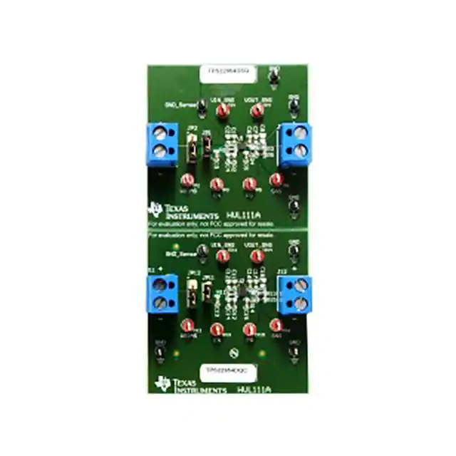
Figure 1. 3D Rendering of EVM
2
TPS22953/54 5.7-V, 5-A, 14-mΩ On-Resistance Load Switch
Copyright © 2015, Texas Instruments Incorporated
SLVUAG1 – March 2015
Submit Documentation Feedback
�Introduction
www.ti.com
1.1
Typical Applications
•
•
•
•
•
•
1.2
Features
•
•
•
•
•
•
•
•
2
Solid State Drives (SSDs)
Embedded/Industrial PC
Ultrabook™/Notebooks
Desktops
Servers
Telecom Systems
VBIAS voltage range: 2.5 V to 5.7 V
VIN input voltage range: 0.7 V to 5.7 V
External capacitor for adjustable rise time
External resistors for adjustable under voltage lockout
External resistors for adjustable voltage supervisor with PG output
High current connection terminals available for 5A maximum continuous switch current operation
Test Point Connections to VIN, VOUT, VBIAS, EN, SNS, and PG pins
SENSE connections for accurate measurement of VIN and VOUT voltages used for Voltage Drop and
ON Resistance Calculations
Electrical Performance
Refer to the datasheet SLVSCJ7 for detailed electrical characteristics of the TPS22953 and TPS22954.
3
Schematic
The Schematic for the TPS22953 and TPS22954 EVMs is shown in Figure 2.
Figure 2. Schematic
SLVUAG1 – March 2015
Submit Documentation Feedback
TPS22953/54 5.7-V, 5-A, 14-mΩ On-Resistance Load Switch
Copyright © 2015, Texas Instruments Incorporated
3
�EVM Connections
4
www.ti.com
EVM Connections
This section describes the connectors, jumpers, and test points on the EVM.
4.1
J1/J11 – VIN Power Connections
These are the high current input connections from the power supply. Connect the positive lead to the top
(+) thermal and the negative lead to the bottom (–) terminal.
4.2
J2/J12 – VOUT Power Connections
These are the high current output connections for loading the EVM. Connect the positive lead of the load
to the top (+) terminal and the GND of the load to the bottom (–) terminal.
4.3
JP1/JP11 – VBIAS Power
These jumpers connect VBIAS to the respective VIN voltage source. VBIAS must be maintained between
2.5 V–5.7 V for proper operation on the TPS22953 and TPS22954 devices. If testing conditions involve
taking the VIN voltage below 2.5V, remove the shunt across JP1/JP11 and connect VBIAS voltage at
TP2/TP12.
4.4
JP2/JP12 – EN Control
These three pin jumpers connect the EN sense resistors either to VIN or to GND. This allow for quickly
enabling/disabling the device after power is present.
4.5
TP1/TP11 – VIN Sense
These connects provide and low current path to the input pins of the device for accurate voltage
measurements. These sense connections should be used when measuring the voltage drop from VIN to
VOUT which is used to calculate the ON resistance. In cases where there is a large load current, it is
recommended configure the power supply to use sense connections. Connect the positive sense lead to
the VIN sense point to overcome voltage drop in cabling.
4.6
TP4/TP14 – VOUT Sense
These connects provide and low current path to the output pins of the device for accurate voltage
measurements. These sense connections should be used when measuring the voltage drop from VIN to
VOUT which is used to calculate the ON resistance.
4.7
TP7/TP17 – GND_Sense
These test points provide a low current path to the GND pad of the device for accurate GND
measurements. In cases where there is a large load current, it is recommended configure the power
supply to use sense connections. Connect the negative sense lead to the GND_sense point to overcome
voltage drop in cabling.
4.8
TP3/TP13 – EN
These test points are used to monitor the EN pin voltage used for UVLO. These test points can also be
used to drive the EN pin independently when JP2/JP12 is removed.
4.9
TP6/TP16 – SNS
These test points are used to monitor the SNS pin voltage.
4.10 TP5/TP15 – PG
These test points are used to monitor the PG pin voltage which is tied to VOUT through at 10kΩ resistor.
4
TPS22953/54 5.7-V, 5-A, 14-mΩ On-Resistance Load Switch
Copyright © 2015, Texas Instruments Incorporated
SLVUAG1 – March 2015
Submit Documentation Feedback
�EVM Connections
www.ti.com
4.11 TP8/TP9/TP10/TP18/TP19/TP20 – GND
These are the GND connection points to the EVM.
4.12 List of Connections
The EVM Connections are summarized in Table 2.
Table 2. EVM Connection Points
5
Connection
Name
Description
J1, J11
VIN
DC input to VIN
J2, J12
VOUT
Load connection for VOU
JP1, JP11
VBIAS Power
Connects VBIAS to VIN
JP2, JP12
EN Control
Connects EN resistors to VIN or GND
TP1, TP11
VIN Sense
Sense connection to VIN
TP2, TP12
VBIAS
VBIAS connection
TP3, TP13
EN
EN connection
TP4, TP14
VOUT Sense
Sense connection to VOUT
TP5, TP15
PG
PG connection
TP6, TP16
SNS
SNS connection
TP7, TP17
GND Sense
Sense connection to device GND
TP8, TP9, TP10, TP18, TP19, TP20
GND
Connection to board ground
Test Setup
This section will describe how to take key parameter measurements on the EVM.
5.1
RON Test Procedure
1.
2.
3.
4.
5.
6.
Setup the EVM per Figure 3.
Set SOURCE1 level to 5.0 V.
Turn on SOURCE1.
Record the voltage reading from METER1 as well as the input current reading from SOURCE1.
Turn SOURCE1 off.
Calculate the Resistance of the switch by dividing the voltage reading from METER1 by the current
reading from SOURCE1.
SLVUAG1 – March 2015
Submit Documentation Feedback
TPS22953/54 5.7-V, 5-A, 14-mΩ On-Resistance Load Switch
Copyright © 2015, Texas Instruments Incorporated
5
�Test Setup
www.ti.com
Figure 3. RON Test Setup
5.2
AC Parameter Test Procedure (tR, tON, tF, tOFF, tD)
1. A detailed description of tR, tON, tF, tOFF, and tD are listed in the TPS22953/54 Datasheet under the
Switching Characteristics Section.
2. The rise time (tR) is selected by the CT capacitor value on each switch channel. The EVM is shipped
with a default CT value of 1 nF.
3. Set up the EVM per Figure 4.
4. Set SOURCE1 level to 5.0 V.
5. Set Signal Generator output to 0–2 Vpp, 10–100 Hz, and 25% duty cycle.
6. Turn SOURCE1 on.
7. Enable the Signal Generator output.
8. Rise time (tR), turn-on time (tON), and delay time (tD) can be observed with a Oscilloscope sync the
scope trigger on the rising edge of the on signal..
9. Fall time (tF) and turn-of time (tOFF) can be observed from the oscilloscope by charging the scope
triggering to sync with the falling edge of the ON signal.
10. Turn SOURCE1 off and disable the signal generator output.
6
TPS22953/54 5.7-V, 5-A, 14-mΩ On-Resistance Load Switch
Copyright © 2015, Texas Instruments Incorporated
SLVUAG1 – March 2015
Submit Documentation Feedback
�Test Setup
www.ti.com
Figure 4. AC Parameter Test Setup
SLVUAG1 – March 2015
Submit Documentation Feedback
TPS22953/54 5.7-V, 5-A, 14-mΩ On-Resistance Load Switch
Copyright © 2015, Texas Instruments Incorporated
7
�Board Assembly and Layout
6
www.ti.com
Board Assembly and Layout
Figure 5. Top Side
8
TPS22953/54 5.7-V, 5-A, 14-mΩ On-Resistance Load Switch
Copyright © 2015, Texas Instruments Incorporated
SLVUAG1 – March 2015
Submit Documentation Feedback
�Board Assembly and Layout
www.ti.com
Figure 6. Bottom Side
SLVUAG1 – March 2015
Submit Documentation Feedback
TPS22953/54 5.7-V, 5-A, 14-mΩ On-Resistance Load Switch
Copyright © 2015, Texas Instruments Incorporated
9
�TPS22953EVM Bill of Materials
7
www.ti.com
TPS22953EVM Bill of Materials
This section contains details on the bill of materials for the TPS22953EVM. Unpopulated items have a
quantity of 0.
Table 3. PS22953EVM Bill of Materials
Designator
Description
Package Reference
Part Number
Manufacturer
C1, C11
Qty
2
CAP, CERM, 1 µF, 16 V, ±10%, X5R, 0603
0603
C1608X5R1C105K
TDK
C3, C13
2
CAP, CERM, 0.01 µF, 50 V, ±5%, X7R, 0603
0603
C0603C103J5RACTU
Kemet
C5, C15
2
CAP, CERM, 1000 pF, 50 V, ±10%, X7R, 0603
0603
C0603C102K5RACTU
Kemet
C6, C16
2
CAP, CERM, 0.1 µF, 25 V, ±10%, X7R, 0603
0603
C1608X7R1E104K
TDK
ED120/2DS
On-Shore Technology
J1, J2, J11, J12
4
TERMINAL BLOCK 5.08MM VERT 2POS, TH
TERM_BLK, 2pos,
5.08mm
JP1, JP11
2
Header, 100mil, 2x1, Gold, TH
Header, 2.54mm, 2x1,
TH
HMTSW-102-07-G-S-240
Samtec
JP2, JP12
2
Header, 100mil, 3x1, Gold, TH
3x1 Header
TSW-103-07-G-S
Samtec
R1, R3, R11, R13
4
RES, 10.0 k, 0.1%, 0.1 W, 0603
0603
RT0603BRD0710KL
Yageo America
R2
1
RES, 1.80 k, 0.1%, 0.1 W, 0603
0603
RT0603BRD071K8L
Yageo America
R4
1
RES, 1.24 k, 0.1%, 0.1 W, 0603
0603
RG1608P-1241-B-T5
Susumu Co Ltd
R5, R15
2
RES, 10.0 k, 1%, 0.1 W, 0603
0603
CRCW060310K0FKEA
Vishay-Dale
R12
1
RES, 3.01 k, 0.1%, 0.1 W, 0603
0603
RT0603BRD073K01L
Yageo America
R14
1
RES, 2.00 k, 0.1%, 0.063 W, 0603
0603
CPF0603B2K0E
TE Connectivity
SH-JP1, SH-JP2,
SH-JP11, SH-JP12
4
Shunt, 100mil, Gold plated, Black
Shunt
969102-0000-DA
3M
TP1, TP2, TP3,
TP4, TP5, TP6,
TP11, TP12, TP13,
TP14, TP15, TP16
12
Test Point, Compact, Red, TH
Red Compact Testpoint 5005
Keystone
TP7, TP8, TP9,
TP10, TP17, TP18,
TP19, TP20
8
Test Point, Miniature, Black, TH
Black Miniature
Testpoint
5001
Keystone
U1
1
5.7V, 5A, 14mΩ On-Resistance Load Switch
DSQ0010A
TPS22953DSQR
Texas Instruments
U2
1
5.7V, 5A, 14mΩ On-Resistance Load Switch
DQC0010A
TPS22953DQCR
Texas Instruments
C2, C12
0
CAP, CERM, 1 µF, 16 V, ±10%, X5R, 0603
0603
C1608X5R1C105K
TDK
C4, C14
0
CAP, CERM, 0.1 µF, 16 V, ±10%, X7R, 0603
0603
C1608X7R1C104K
TDK
C7, C17
0
CAP, CERM, 0.1 µF, 25 V, ±10%, X7R, 0603
0603
C1608X7R1E104K
TDK
C8, C18
0
CAP, CERM, 10 µF, 16 V, ±10%, X6S, 0805
0805
C2012X6S1C106MT
TDK
10
TPS22953/54 5.7-V, 5-A, 14-mΩ On-Resistance Load Switch
Copyright © 2015, Texas Instruments Incorporated
SLVUAG1 – March 2015
Submit Documentation Feedback
�TPS22954EVM Bill of Materials
www.ti.com
8
TPS22954EVM Bill of Materials
This section contains details on the bill of materials for the TPS22954EVM. Unpopulated items have a
quantity of 0.
Table 4. TPS22954EVM Bill of Materials
Designator
Description
PackageReference
PartNumber
Manufacturer
C1, C11
Qty
2
CAP, CERM, 1 µF, 16 V, ±10%, X5R, 0603
0603
C1608X5R1C105K
TDK
C3, C13
2
CAP, CERM, 0.01 µF, 50 V, ±5%, X7R, 0603
0603
C0603C103J5RACTU
Kemet
C5, C15
2
CAP, CERM, 1000 pF, 50 V, ±10%, X7R,
0603
0603
C0603C102K5RACTU
Kemet
C6, C16
2
CAP, CERM, 0.1 µF, 25 V, ±10%, X7R, 0603
0603
C1608X7R1E104K
TDK
ED120/2DS
On-Shore Technology
J1, J2, J11, J12
4
TERMINAL BLOCK 5.08MM VERT 2POS, TH
TERM_BLK, 2pos,
5.08mm
JP1, JP11
2
Header, 100mil, 2x1, Gold, TH
Header, 2.54mm, 2x1,
TH
HMTSW-102-07-G-S-240
Samtec
JP2, JP12
2
Header, 100mil, 3x1, Gold, TH
3x1 Header
TSW-103-07-G-S
Samtec
R1, R3, R11, R13
4
RES, 10.0 k, 0.1%, 0.1 W, 0603
0603
RT0603BRD0710KL
Yageo America
R2
1
RES, 1.80 k, 0.1%, 0.1 W, 0603
0603
RT0603BRD071K8L
Yageo America
R4
1
RES, 1.24 k, 0.1%, 0.1 W, 0603
0603
RG1608P-1241-B-T5
Susumu Co Ltd
R5, R15
2
RES, 10.0 k, 1%, 0.1 W, 0603
0603
CRCW060310K0FKEA
Vishay-Dale
R12
1
RES, 3.01 k, 0.1%, 0.1 W, 0603
0603
RT0603BRD073K01L
Yageo America
R14
1
RES, 2.00 k, 0.1%, 0.063 W, 0603
0603
CPF0603B2K0E
TE Connectivity
SH-JP1, SH-JP2,
SH-JP11, SH-JP12
4
Shunt, 100mil, Gold plated, Black
Shunt
969102-0000-DA
3M
TP1, TP2, TP3,
TP4, TP5, TP6,
TP11, TP12, TP13,
TP14, TP15, TP16
12
Test Point, Compact, Red, TH
Red Compact Testpoint
5005
Keystone
TP7, TP8, TP9,
TP10, TP17, TP18,
TP19, TP20
8
Test Point, Miniature, Black, TH
Black Miniature Testpoint 5001
Keystone
U1
1
5.7V, 5A, 14mΩ On-Resistance Load Switch
DSQ0010A
TPS22954DSQR
Texas Instruments
U2
1
5.7V, 5A, 14mΩ On-Resistance Load Switch
DQC0010A
TPS22954DQCR
Texas Instruments
C2, C12
0
CAP, CERM, 1 µF, 16 V, ±10%, X5R, 0603
0603
C1608X5R1C105K
TDK
C4, C14
0
CAP, CERM, 0.1 µF, 16 V, ±10%, X7R, 0603
0603
C1608X7R1C104K
TDK
C7, C17
0
CAP, CERM, 0.1 µF, 25 V, ±10%, X7R, 0603
0603
C1608X7R1E104K
TDK
C8, C18
0
CAP, CERM, 10 µF, 16 V, ±10%, X6S, 0805
0805
C2012X6S1C106MT
TDK
SLVUAG1 – March 2015
Submit Documentation Feedback
TPS22953/54 5.7-V, 5-A, 14-mΩ On-Resistance Load Switch
Copyright © 2015, Texas Instruments Incorporated
11
�IMPORTANT NOTICE
Texas Instruments Incorporated and its subsidiaries (TI) reserve the right to make corrections, enhancements, improvements and other
changes to its semiconductor products and services per JESD46, latest issue, and to discontinue any product or service per JESD48, latest
issue. Buyers should obtain the latest relevant information before placing orders and should verify that such information is current and
complete. All semiconductor products (also referred to herein as “components”) are sold subject to TI’s terms and conditions of sale
supplied at the time of order acknowledgment.
TI warrants performance of its components to the specifications applicable at the time of sale, in accordance with the warranty in TI’s terms
and conditions of sale of semiconductor products. Testing and other quality control techniques are used to the extent TI deems necessary
to support this warranty. Except where mandated by applicable law, testing of all parameters of each component is not necessarily
performed.
TI assumes no liability for applications assistance or the design of Buyers’ products. Buyers are responsible for their products and
applications using TI components. To minimize the risks associated with Buyers’ products and applications, Buyers should provide
adequate design and operating safeguards.
TI does not warrant or represent that any license, either express or implied, is granted under any patent right, copyright, mask work right, or
other intellectual property right relating to any combination, machine, or process in which TI components or services are used. Information
published by TI regarding third-party products or services does not constitute a license to use such products or services or a warranty or
endorsement thereof. Use of such information may require a license from a third party under the patents or other intellectual property of the
third party, or a license from TI under the patents or other intellectual property of TI.
Reproduction of significant portions of TI information in TI data books or data sheets is permissible only if reproduction is without alteration
and is accompanied by all associated warranties, conditions, limitations, and notices. TI is not responsible or liable for such altered
documentation. Information of third parties may be subject to additional restrictions.
Resale of TI components or services with statements different from or beyond the parameters stated by TI for that component or service
voids all express and any implied warranties for the associated TI component or service and is an unfair and deceptive business practice.
TI is not responsible or liable for any such statements.
Buyer acknowledges and agrees that it is solely responsible for compliance with all legal, regulatory and safety-related requirements
concerning its products, and any use of TI components in its applications, notwithstanding any applications-related information or support
that may be provided by TI. Buyer represents and agrees that it has all the necessary expertise to create and implement safeguards which
anticipate dangerous consequences of failures, monitor failures and their consequences, lessen the likelihood of failures that might cause
harm and take appropriate remedial actions. Buyer will fully indemnify TI and its representatives against any damages arising out of the use
of any TI components in safety-critical applications.
In some cases, TI components may be promoted specifically to facilitate safety-related applications. With such components, TI’s goal is to
help enable customers to design and create their own end-product solutions that meet applicable functional safety standards and
requirements. Nonetheless, such components are subject to these terms.
No TI components are authorized for use in FDA Class III (or similar life-critical medical equipment) unless authorized officers of the parties
have executed a special agreement specifically governing such use.
Only those TI components which TI has specifically designated as military grade or “enhanced plastic” are designed and intended for use in
military/aerospace applications or environments. Buyer acknowledges and agrees that any military or aerospace use of TI components
which have not been so designated is solely at the Buyer's risk, and that Buyer is solely responsible for compliance with all legal and
regulatory requirements in connection with such use.
TI has specifically designated certain components as meeting ISO/TS16949 requirements, mainly for automotive use. In any case of use of
non-designated products, TI will not be responsible for any failure to meet ISO/TS16949.
Products
Applications
Audio
www.ti.com/audio
Automotive and Transportation
www.ti.com/automotive
Amplifiers
amplifier.ti.com
Communications and Telecom
www.ti.com/communications
Data Converters
dataconverter.ti.com
Computers and Peripherals
www.ti.com/computers
DLP® Products
www.dlp.com
Consumer Electronics
www.ti.com/consumer-apps
DSP
dsp.ti.com
Energy and Lighting
www.ti.com/energy
Clocks and Timers
www.ti.com/clocks
Industrial
www.ti.com/industrial
Interface
interface.ti.com
Medical
www.ti.com/medical
Logic
logic.ti.com
Security
www.ti.com/security
Power Mgmt
power.ti.com
Space, Avionics and Defense
www.ti.com/space-avionics-defense
Microcontrollers
microcontroller.ti.com
Video and Imaging
www.ti.com/video
RFID
www.ti-rfid.com
OMAP Applications Processors
www.ti.com/omap
TI E2E Community
e2e.ti.com
Wireless Connectivity
www.ti.com/wirelessconnectivity
Mailing Address: Texas Instruments, Post Office Box 655303, Dallas, Texas 75265
Copyright © 2015, Texas Instruments Incorporated
�


 工商网监
湘ICP备2023018690号
工商网监
湘ICP备2023018690号
