Product
Folder
Sample &
Buy
Support &
Community
Tools &
Software
Technical
Documents
TPS22961
SLVSCI4B – FEBRUARY 2014 – REVISED SEPTEMBER 2014
TPS22961 3.5-V, 6-A, Ultra-low Resistance Load Switch
1 Features
3 Description
•
•
•
•
The TPS22961 is a small, ultra-low RON, single
channel load switch with controlled turn on. The
device contains an N-channel MOSFET that can
operate over an input voltage range of 0.8 V to 3.5 V
and supports a maximum continuous current of 6 A.
1
•
•
•
•
•
•
•
Integrated Single Channel Load Switch
VBIAS Voltage Range: 3 V to 5.5 V
Input Voltage Range: 0.8 V to 3.5 V
Ultra low RON Resistance
– RON = 4.4 mΩ at VIN = 1.05 V (VBIAS = 5 V)
6A Maximum Continuous Switch Current
Low Quiescent Current < 1 µA (max)
Low Control Input Threshold Enables use of 1.2V/1.8-V/2.5-V/3.3-V Logic
Controlled Slew Rate
– tR = 4.2 µs at VIN = 1.05 V (VBIAS = 5 V)
Quick Output Discharge (QOD)
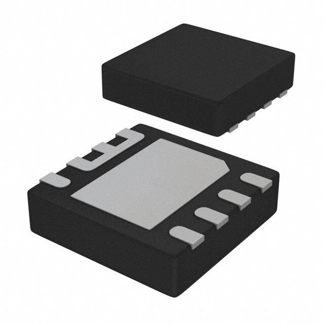
SON 8-terminal Package with Thermal Pad
ESD Performance Tested per JESD 22
– 2-kV HBM and 1-kV CDM
The TPS22961 is available in a small, space-saving 3
mm x 3 mm 8-SON package (DNY) with integrated
thermal pad allowing for high power dissipation. The
device is characterized for operation over the free-air
temperature range of –40°C to 85°C.
2 Applications
•
•
•
•
•
•
The combination of ultra-low RON and high current
capability of the device makes it ideal for driving
processor rails with very tight voltage dropout
tolerances. Quick rise time of the device allows for
power rails to come up quickly when the device is
enabled, thereby reducing response time for power
distribution. The switch can be independently
controlled via the ON terminal, which is capable of
interfacing directly with low-voltage control signals
originating from microcontrollers or low voltage
discrete logic. The device further reduces the total
solution size by integrating a 260 Ω pull-down
transistor for quick output discharge (QOD) when the
switch is turned off.
Ultrabook™/Notebooks
Desktops
Servers
Set-top Boxes
Telecom Systems
Tablet PC
Device Information(1)
PART NUMBER
PACKAGE
TPS22961
BODY SIZE
WSON (8)
3.00 mm x 3.00 mm
(1) For all available packages, see the orderable addendum at
the end of the datasheet.
4 Simplified Schematic
VBIAS
(4.5V to 5.5V)
VIN
Power
Supply
Processor
(x86, FPGA,
DSP)
VOUT
CIN
RON vs VIN (VBIAS = 5 V, IOUT = –200 mA)
8
CL
7
ON
OFF
ON
GND
6
TPS22961
RON (m
)
5
Typical Application: driving high current
core rails for a processor
4
3
2
-40C
1
25C
85C
0
0.8
1
1.2
1.4
1.6
1.8
2
2.2
2.4
2.6
2.8
3
VIN (V)
C007
1
An IMPORTANT NOTICE at the end of this data sheet addresses availability, warranty, changes, use in safety-critical applications,
intellectual property matters and other important disclaimers. PRODUCTION DATA.
�TPS22961
SLVSCI4B – FEBRUARY 2014 – REVISED SEPTEMBER 2014
www.ti.com
Table of Contents
1
2
3
4
5
6
7
8
Features ..................................................................
Applications ...........................................................
Description .............................................................
Simplified Schematic.............................................
Revision History.....................................................
Terminal Configuration and Functions................
Specifications.........................................................
1
1
1
1
2
3
3
7.1
7.2
7.3
7.4
7.5
7.6
7.7
7.8
3
4
4
4
5
5
6
8
Absolute Maximum Ratings ......................................
Handling Ratings.......................................................
Recommended Operating Conditions.......................
Thermal Information ..................................................
Electrical Characteristics, VBIAS = 5.0 V ...................
Electrical Characteristics, VBIAS = 3.0 V ...................
Switching Characteristics ..........................................
Typical Characteristics ..............................................
Detailed Description ............................................ 12
8.1 Overview ................................................................. 12
8.2 Functional Block Diagram ....................................... 12
8.3 Feature Description................................................. 13
9
Applications and Implementation ...................... 14
9.1 Application Information............................................ 14
9.2 Typical Application .................................................. 14
10 Power Supply Recommendations ..................... 18
11 Layout................................................................... 19
11.1 Layout Guidelines ................................................. 19
11.2 Layout Example .................................................... 19
12 Device and Documentation Support ................. 20
12.1 Trademarks ........................................................... 20
12.2 Electrostatic Discharge Caution ............................ 20
12.3 Glossary ................................................................ 20
13 Mechanical, Packaging, and Orderable
Information ........................................................... 20
5 Revision History
Changes from Revision A (February 2014) to Revision B
•
Fixed caption error in Filtered Output curve. ....................................................................................................................... 18
Changes from Original (February 2014) to Revision A
•
2
Page
Page
Initial release of full version. .................................................................................................................................................. 1
Submit Documentation Feedback
Copyright © 2014, Texas Instruments Incorporated
Product Folder Links: TPS22961
�TPS22961
www.ti.com
SLVSCI4B – FEBRUARY 2014 – REVISED SEPTEMBER 2014
6 Terminal Configuration and Functions
DNY PACKAGE
8 TERMINAL
VIN
1
VIN
2
VIN
8
VOUT
VOUT
8
7
VOUT
VOUT
7
(Exposed thermal
VBIAS
3
ON
4
pad)
VIN
1
VIN
2
VIN
3
VBIAS
4
ON
(Exposed thermal
6
VOUT
VOUT
6
5
GND
GND
5
Top View
pad)
Bottom View
Pin Functions
PIN
I/O
DESCRIPTION
NAME
NO.
VIN
1, 2
I
Switch input. Place ceramic bypass capacitor(s) between this terminal and GND. See Detailed
Description section for more information.
VIN
Exposed thermal
Pad
I
Switch input. Place ceramic bypass capacitor(s) between this terminal and GND. See Detailed
Description section for more information.
VBIAS
3
I
Bias voltage. Power supply to the device.
ON
4
I
Active high switch control input. Do not leave floating.
GND
5
–
Ground.
VOUT
6, 7, 8
O
Switch output. Place ceramic bypass capacitor(s) between this terminal and GND. See Detailed
Description section for more information.
7 Specifications
7.1 Absolute Maximum Ratings
Over operating free-air temperature range (unless otherwise noted) (1)
MIN
MAX
VIN
Input voltage range
–0.3
4
V
VBIAS
Bias voltage range
–0.3
6
V
VOUT
Output voltage range
–0.3
4
V
VON
ON pin voltage range
–0.3
6
V
IMAX
Maximum Continuous Switch Current
6
A
IPLS
Maximum Pulsed Switch Current, pulse < 300 µs, 2% duty cycle
TA
Operating free-air temperature range
TJ
Maximum junction temperature
(1)
–40
UNIT
8
A
85
°C
125
°C
Stresses beyond those listed under Absolute Maximum Ratings may cause permanent damage to the device. These are stress ratings
only, which do not imply functional operation of the device at these or any other conditions beyond those indicated under Recommended
Operating Conditions. Exposure to absolute-maximum-rated conditions for extended periods may affect device reliability.
Submit Documentation Feedback
Copyright © 2014, Texas Instruments Incorporated
Product Folder Links: TPS22961
3
�TPS22961
SLVSCI4B – FEBRUARY 2014 – REVISED SEPTEMBER 2014
www.ti.com
7.2 Handling Ratings
TSTG
Storage temperature range
TLEAD
Maximum lead temperature (10-s soldering time)
VESD
(1)
(2)
(3)
(1)
MIN
MAX
UNIT
–65
150
°C
300
°C
Human-Body Model (HBM) (2)
2
kV
Charged-Device Model (CDM) (3)
1
kV
Electrostatic discharge (ESD) to measure device sensitivity and immunity to damage caused by assembly line electrostatic discharges in
to the device.
Level listed above is the passing level per ANSI, ESDA, and JEDEC JS-001. JEDEC document JEP155 states that 500-V HBM allows
safe manufacturing with a standard ESD control process.
Level listed above is the passing level per EIA-JEDEC JESD22-C101. JEDEC document JEP157 states that 250-V CDM allows safe
manufacturing with a standard ESD control process.
7.3 Recommended Operating Conditions
Over operating free-air temperature range (unless otherwise noted)
MIN
MAX
VIN
Input voltage range
0.8
VBIAS – 1.95
V
VBIAS
Bias voltage range
3
5.5
V
VON
ON voltage range
0
VOUT
Output voltage range
VIH,
ON
High-level voltage, ON
VBIAS = 3 V to 5.5 V
VIL, ON
Low-level voltage, ON
VBIAS = 3 V to 5.5 V
CIN
Input Capacitor
(1)
UNIT
5.5
V
VIN
V
1.2
5.5
V
0
0.5
1 (1)
V
µF
Refer to Detailed Description section.
7.4 Thermal Information
TPS22961
THERMAL METRIC (1)
DNY
UNIT
8 PINS
θJA
Junction-to-ambient thermal resistance
44.6
θJCtop
Junction-to-case (top) thermal resistance
44.4
θJB
Junction-to-board thermal resistance
17.6
ψJT
Junction-to-top characterization parameter
0.4
ψJB
Junction-to-board characterization parameter
17.4
θJCbot
Junction-to-case (bottom) thermal resistance
1.1
(1)
4
°C/W
For more information about traditional and new thermal metrics, see the IC Package Thermal Metrics application report, SPRA953.
Submit Documentation Feedback
Copyright © 2014, Texas Instruments Incorporated
Product Folder Links: TPS22961
�TPS22961
www.ti.com
SLVSCI4B – FEBRUARY 2014 – REVISED SEPTEMBER 2014
7.5 Electrical Characteristics, VBIAS = 5.0 V
Unless otherwise noted, the specification in the following table applies over the operating ambient temperature
–40°C ≤ TA ≤ 85°C (full) and VBIAS = 5.0 V. Typical values are for TA = 25°C (unless otherwise noted).
PARAMETER
TEST CONDITIONS
TA
MIN
TYP
MAX
UNIT
POWER SUPPLIES AND CURRENTS
IQ, VBIAS
VBIAS quiescent current
IOUT = 0, VIN = 3 V,
VON = VBIAS = 5.0 V
Full
0.6
1
µA
ISD, VBIAS
VBIAS shutdown current
VON = 0 V, VOUT = 0 V
Full
0.6
1
µA
VIN = 3.0 V
0.0009
0.1
VIN = 2.5 V
0.0008
0.1
0.0007
0.1
VIN = 1.05 V
0.0007
0.1
VIN = 0.8 V
0.0006
0.1
ISD, VIN
ION
VIN shutdown current
ON terminal input leakage
current
VON = 0 V,
VOUT = 0 V
VIN = 2.0 V
VON = 5.5 V
Full
Full
0.1
µA
µA
RESISTANCE CHARACTERISTICS
VIN = 3.0 V
VIN = 2.5 V
RON
ON-state resistance
IOUT = –200 mA,
VBIAS = 5.0 V
VIN = 2.0 V
VIN = 1.05 V
VIN = 0.8 V
RPD
Output pulldown resistance
VIN = 5.0 V, VON = 0 V, VOUT = 1 V
25°C
6.5
Full
8
8.8
25°C
5.3
Full
6.3
7.2
25°C
4.8
Full
5.8
6.7
25°C
4.4
Full
5.3
6.2
25°C
4.3
Full
5.3
6.1
Full
mΩ
mΩ
mΩ
mΩ
mΩ
300
Ω
TYP
MAX
UNIT
0.3
1
µA
µA
260
7.6 Electrical Characteristics, VBIAS = 3.0 V
Unless otherwise noted, the specification in the following table applies over the operating ambient temperature
–40°C ≤ TA ≤ 85°C (full) and VBIAS = 3.0 V. Typical values are for TA = 25°C unless otherwise noted.
PARAMETER
TEST CONDITIONS
TA
MIN
POWER SUPPLIES AND CURRENTS
IQ, VBIAS
VBIAS quiescent current
IOUT = 0, VIN = 1 V,
VON = VBIAS = 3.0 V
ISD, VBIAS
VBIAS shutdown current
VON = 0 V, VOUT = 0 V
ISD, VIN
VIN shutdown current
VON = 0 V,
VOUT = 0 V
ION
ON terminal input leakage
current
VON = 5.5 V
Full
Full
VIN = 1.05 V
VIN = 0.8 V
Full
0.3
1
0.001
0.1
0.0008
0.1
Full
0.1
µA
µA
RESISTANCE CHARACTERISTICS
RON
RPD
ON-state resistance
Output pull-down resistance
IOUT = –200 mA,
VBIAS = 3.0 V
VIN =1.05 V
VIN = 0.8 V
VIN = 3V, VON = 0 V, VOUT = 1 V
25°C
6.7
Full
25°C
9.2
5.8
Full
Full
8.4
7.0
7.9
260
300
Submit Documentation Feedback
Copyright © 2014, Texas Instruments Incorporated
Product Folder Links: TPS22961
mΩ
mΩ
Ω
5
�TPS22961
SLVSCI4B – FEBRUARY 2014 – REVISED SEPTEMBER 2014
www.ti.com
7.7 Switching Characteristics
Refer to the timing test circuit in Figure 1 (unless otherwise noted) for references to external components used for the test
condition in the switching characteristics table.
PARAMETER
TEST CONDITION
MIN
TYP
MAX
UNIT
VIN = 2.5 V, VON = VBIAS = 5 V, TA = 25ºC (unless otherwise noted)
tON
Turn-on time
tOFF
Turn-off time
10.0
tR
VOUT rise time
tF
VOUT fall time
2.0
tD
Delay time
8.1
3.5
RL = 10 Ω, CL = 0.1 µF
6.3
µs
VIN = 1.05 V, VON = VBIAS = 5 V, TA = 25ºC (unless otherwise noted)
tON
Turn-on time
tOFF
Turn-off time
tR
VOUT rise time
tF
VOUT fall time
tD
Delay time
L = 2.2 µH (DCR = 0.33 Ω),
C = 2 x 22 µF
(Refer to Typical Application
Powering Rails Sensitive to Ringing
and Overvoltage due to Fast Rise
Time and Figure 31)
8.1
11.3
17.3
13700
5
9.5
12.5
µs
44200
6.7
9.3
12.5
VIN = 0.8 V, VON = VBIAS = 5 V, TA = 25ºC (unless otherwise noted)
tON
Turn-on time
9.7
tOFF
Turn-off time
6.0
tR
VOUT rise time
tF
VOUT fall time
1.8
tD
Delay time
8.1
RL = 10 Ω, CL = 0.1 µF
3.2
µs
VIN = 1.05 V, VON = 5 V, VBIAS = 3.0 V, TA = 25ºC (unless otherwise noted)
tON
Turn-on time
19.1
tOFF
Turn-off time
4.7
tR
VOUT rise time
tF
VOUT fall time
tD
Delay time
RL = 10 Ω, CL = 0.1 µF
9.0
µs
2.0
15.6
VIN = 0.8 V, VON = 5 V, VBIAS = 3.0 V, TA = 25ºC (unless otherwise noted)
tON
Turn-on time
tOFF
Turn-off time
tR
VOUT rise time
tF
VOUT fall time
tD
Delay time
6
19.0
5.4
RL = 10 Ω, CL = 0.1 µF
7.0
µs
1.9
15.7
Submit Documentation Feedback
Copyright © 2014, Texas Instruments Incorporated
Product Folder Links: TPS22961
�TPS22961
www.ti.com
SLVSCI4B – FEBRUARY 2014 – REVISED SEPTEMBER 2014
VOUT
VIN
CIN = 1µF
ON
+
-
(A)
CL
ON
RL
OFF
VBIAS
GND
TPS22961
GND
GND
Timing Test Circuit
VON
50%
50%
tOFF
tON
VOUT
50%
50%
tF
tR
90%
VOUT
10%
10%
90%
10%
tD
Timing Waveforms
(A) Rise and fall times of the control signal is 100ns.
Figure 1. Switching Characteristics Measurement Setup and Definitions
Submit Documentation Feedback
Copyright © 2014, Texas Instruments Incorporated
Product Folder Links: TPS22961
7
�TPS22961
SLVSCI4B – FEBRUARY 2014 – REVISED SEPTEMBER 2014
www.ti.com
0.9
0.9
0.8
0.8
0.7
0.7
0.6
0.6
0.5
0.5
ISD,VBIAS (�A)
IQ,VBIAS (
A)
7.8 Typical Characteristics
0.4
0.3
0.4
0.3
0.2
0.2
-40C
0.1
-40C
0.1
25C
25C
85C
85C
0
0
3
3.25
3.5
3.75
4
4.25
4.5
4.75
5
5.25
5.5
3
3.25
3.5
3.75
4
4.25
VBIAS (V)
4.5
4.75
5
5.25
VIN = 1.05 V
VON = 5 V
C003
IOUT = 0 A
VON = 0 V
Figure 2. IQ,VBIAS vs VBIAS
0.04
5.5
VBIAS (V)
C002
VOUT = 0 V
Figure 3. ISD,VBIAS vs VBIAS
8
-40C
25C
7
85C
0.03
6
0.025
5
RON (m
)
ISD,VIN (
A)
0.035
0.02
4
0.015
3
0.01
2
0.005
1
0
0
VIN = 0.8V
0.8
1
1.2
1.4
1.6
1.8
2
2.2
2.4
2.6
2.8
3
VIN = 0.9V
VIN = 1.05V
-40
-15
10
VIN (V)
35
60
85
Ambient Temperature (£C)
C001
VBIAS = 5 V
VON = 0 V
VOUT = 0 V
C004
VBIAS = 3 V
8
7
7
6
6
5
5
4
VIN = 0.8V
VIN = 1.05V
3
IOUT = –200 mA
Figure 5. RON vs Ambient Temperature
8
RON (m
)
RON (m
)
Figure 4. ISD,VIN vs VIN
VON = 5 V
4
3
VIN = 1.2V
2
2
VIN = 1.5V
-40C
VIN = 1.8V
1
1
VIN = 2.5V
25C
85C
VIN = 3V
0
0
-40
-15
10
35
60
85
0.8
Ambient Temperature (C)
0.85
0.9
0.95
VON = 5 V
IOUT = –200 mA
C006
VBIAS = 3 V
Figure 6. RON vs Ambient Temperature
8
1.05
VIN (V)
C005
VBIAS = 5 V
1
Submit Documentation Feedback
VON = 5 V
IOUT = –200 mA
Figure 7. RON vs VIN
Copyright © 2014, Texas Instruments Incorporated
Product Folder Links: TPS22961
�TPS22961
www.ti.com
SLVSCI4B – FEBRUARY 2014 – REVISED SEPTEMBER 2014
Typical Characteristics (continued)
8
8
7
6
6
RON (m
)
RON (m
)
5
4
4
3
2
2
-40C
1
VBIAS = 3V
25C
VBIAS = 5V
85C
0
0
0.8
1
1.2
1.4
1.6
1.8
2
2.2
2.4
2.6
2.8
3
0.8
1
1.2
1.4
1.6
VIN (V)
1.8
2
2.2
2.4
2.6
2.8
C007
VBIAS = 5 V
3
VIN (V)
VON = 5 V
C008
IOUT = –200 mA
TA = 25°C
VON = 5 V
Figure 8. RON vs VIN
IOUT = –200 mA
Figure 9. RON vs VIN
8
270
268
7
266
6
5
262
RON (m
)
RPD (
)
264
260
258
4
3
256
2
254
-40C
-40C
1
25C
252
25C
85C
85C
0
250
3
3.5
4
4.5
0.8
5
1
1.2
1.4
1.6
1.8
2
2.2
2.4
2.6
2.8
C012
C009
VON = 0 V
VIN = 1.05 V
VOUT = 1 V
VBIAS = 5 V
Figure 10. RPD vs VBIAS
VON = 5 V
IOUT = –6 A
Figure 11. RON vs VIN at 6A load
1
1.1
0.95
1.05
0.9
1
VIH,ON (V)
VIL,ON (V)
3
VIN (V)
VBIAS (V)
0.85
0.95
0.9
0.8
-40C
0.75
-40C
0.85
25C
25C
85C
85C
0.8
0.7
3
3.5
4
4.5
5
3
3.5
4
4.5
5
VBIAS (V)
VBIAS (V)
C011
C010
VIN = VBIAS – 2 V
VIN = VBIAS – 2 V
Figure 13. VIH,ON vs VBIAS
Figure 12. VIL,ON vs VBIAS
Submit Documentation Feedback
Copyright © 2014, Texas Instruments Incorporated
Product Folder Links: TPS22961
9
�TPS22961
SLVSCI4B – FEBRUARY 2014 – REVISED SEPTEMBER 2014
www.ti.com
Typical Characteristics (continued)
19
10
18
9.5
17
9
16
tD (
s)
tD (
s)
8.5
15
14
8
7.5
13
7
12
-40C
11
-40C
6.5
25C
25C
85C
10
0.80
85C
6
0.83
0.85
0.88
0.90
0.93
0.95
0.98
1.00
1.03
0.8
1.05
1
1.2
1.4
1.6
1.8
2
2.2
2.4
2.6
2.8
C015
RL = 10 Ω
VBIAS = 3 V
3
VIN (V)
VIN (V)
CL = 0.1 µF
C020
RL = 10 Ω
VBIAS = 5 V
Figure 14. tD vs VIN
CL = 0.1 µF
Figure 15. tD vs VIN
2.2
2.4
2.3
2.1
2.2
2
2.1
1.9
tF (
s)
tF (
s)
2
1.9
1.8
1.8
1.7
1.7
1.6
1.6
-40C
-40C
1.5
25C
1.5
25C
85C
85C
1.4
0.80
1.4
0.83
0.85
0.88
0.90
0.93
0.95
0.98
1.00
1.03
0.8
1.05
1
1.2
1.4
1.6
1.8
2
2.2
2.4
2.6
2.8
C014
RL = 10 Ω
VBIAS = 3 V
3
VIN (V)
VIN (V)
CL = 0.1 µF
C021
RL = 10 Ω
VBIAS = 5 V
Figure 16. tF vs VIN
CL = 0.1 µF
Figure 17. tF vs VIN
8
7.5
7
7
6.5
6
6
tOFF (
s)
tOFF (
s)
5.5
5
5
4
4.5
3
4
3.5
-40C
-40C
2
25C
25C
3
85C
85C
2.5
0.80
0.83
0.85
0.88
0.90
0.93
0.95
0.98
VIN (V)
VBIAS = 3 V
RL = 10 Ω
1.00
1.03
1
1.05
0.8
1.2
1.4
1.6
1.8
2
2.2
2.4
C016
CL = 0.1 µF
2.6
2.8
3
VIN (V)
C019
VBIAS = 5 V
Figure 18. tOFF vs VIN
10
1
RL = 10 Ω
CL = 0.1 µF
Figure 19. tOFF vs VIN
Submit Documentation Feedback
Copyright © 2014, Texas Instruments Incorporated
Product Folder Links: TPS22961
�TPS22961
www.ti.com
SLVSCI4B – FEBRUARY 2014 – REVISED SEPTEMBER 2014
Typical Characteristics (continued)
24
12
11.5
22
11
10.5
20
tON (
s)
tON (�s)
10
18
9.5
9
16
8.5
8
-40C
14
25C
-40C
25C
7.5
85C
12
0.80
85C
7
0.83
0.85
0.88
0.90
0.93
0.95
0.98
1.00
1.03
1.05
0.8
1
1.2
1.4
1.6
VIN (V)
1.8
2
2.2
2.4
2.6
2.8
C017
RL = 10 Ω
VBIAS = 3 V
3
VIN (V)
C018
CL = 0.1 µF
RL = 10 Ω
VBIAS = 5 V
Figure 20. tON vs VIN
CL = 0.1 µF
Figure 21. tON vs VIN
12
10
11
9
10
8
9
tR (
s)
tR (
S)
7
8
7
6
5
6
4
5
-40C
4
-40C
3
25C
25C
85C
3
0.80
85C
2
0.83
0.85
0.88
0.90
0.93
0.95
0.98
1.00
1.03
1.05
0.8
1
1.2
1.4
VIN (V)
1.6
1.8
2
2.2
2.4
2.8
3
VIN (V)
C013
VBIAS = 3 V
2.6
RL = 10 Ω
C022
CL = 0.1 µF
RL = 10 Ω
VBIAS = 5 V
Figure 22. tR vs VIN
CL = 0.1 µF
Figure 23. tR vs VIN
11
tR (
s)
9
7
5
VBIAS = 3.0V
VBIAS = 3.3V
VBIAS = 3.6V
VBIAS = 4.2V
VBIAS = 5.0V
VBIAS = 5.5V
3
1
0.8
1
1.2
1.4
1.6
1.8
2
2.2
2.4
2.6
2.8
3
VIN (V)
C023
TA = 25°C
RL = 10 Ω
CL = 0.1 µF
Figure 24. tR vs VIN for Various VBIAS
Submit Documentation Feedback
Copyright © 2014, Texas Instruments Incorporated
Product Folder Links: TPS22961
11
�TPS22961
SLVSCI4B – FEBRUARY 2014 – REVISED SEPTEMBER 2014
www.ti.com
8 Detailed Description
8.1 Overview
The device is a 3.5 V, 6 A load switch in a 8-terminal SON package. To reduce voltage drop for low voltage and
high current rails, the device implements an ultra-low resistance N-channel MOSFET which reduces the drop out
voltage through the device at very high currents.
The device has a controlled, yet quick, fixed slew rate for applications that require quick turn-on response. During
shutdown, the device has very low leakage currents, thereby reducing unnecessary leakages for downstream
modules during standby. Integrated control logic, driver, and output discharge FET eliminates the need for any
external components, which reduces solution size and BOM count.
8.2 Functional Block Diagram
VIN
VBIAS
ON
Control
Logic
Driver
VOUT
GND
12
Submit Documentation Feedback
Copyright © 2014, Texas Instruments Incorporated
Product Folder Links: TPS22961
�TPS22961
www.ti.com
SLVSCI4B – FEBRUARY 2014 – REVISED SEPTEMBER 2014
8.3 Feature Description
8.3.1 On/off Control
The ON terminal controls the state of the load switch, and asserting the terminal high (active high) enables the
switch. The ON terminal is compatible with standard GPIO logic threshold and can be used with any
microcontroller or discrete logic with 1.2 V or higher GPIO voltage. This terminal cannot be left floating and must
be tied either high or low for proper functionality.
8.3.2
Input Capacitor (CIN)
To limit the voltage drop on the input supply caused by transient in-rush currents when the switch turns on into a
discharged load capacitor or short-circuit, a capacitor needs to be placed between VIN and GND. A 1 µF ceramic
capacitor, CIN, placed close to the terminals, is usually sufficient. Higher values of CIN can be used to further
reduce the voltage drop in high-current application. When switching heavy loads, it is recommended to have an
input capacitor 10 times higher than the output capacitor to avoid excessive voltage drop.
8.3.3 Output Capacitor (CL)
Due to the integrated body diode in the NMOS switch, a CIN greater than CL is highly recommended. A CL
greater than CIN can cause VOUT to exceed VIN when the system supply is removed. This could result in current
flow through the body diode from VOUTT to VIN. A CIN to CL ratio of 10 to 1 is recommended for minimizing VIN
dip caused by inrush currents during startup, however a 10 to 1 ratio for capacitance is not required for proper
functionality of the device. A ratio smaller than 10 to 1 (such as 1 to 1) could cause a VIN dip upon turn-on due to
inrush currents.
8.3.4 VIN and VBIAS Voltage Range
For optimal RON performance, make sure VIN ≤ (VBIAS – 1.95 V). For example, in order to have VIN = 3.5V, VBIAS
must be 5.5 V. The device will still be functional if VIN > (VBIAS – 1.95 V) but it will exhibit RON greater than what is
listed in the Electrical Characteristics, VBIAS = 5.0 V table. See Figure 25 for an example of a typical device.
Notice the increasing RON as VIN increases. Be sure to never exceed the maximum voltage rating for VIN and
VBIAS.
10
9
RON (m
)
8
7
6
VBIAS = 3.0V
VBIAS = 3.3V
VBIAS = 3.6V
VBIAS = 4.2V
VBIAS = 5.0V
VBIAS = 5.5V
5
4
0.8
1.2
1.6
2
2.4
2.8
3.2
3.6
4
4.4
4.8
5.2
VIN (V)
C023
Figure 25. RON vs VIN (VIN > VBIAS)
Submit Documentation Feedback
Copyright © 2014, Texas Instruments Incorporated
Product Folder Links: TPS22961
13
�TPS22961
SLVSCI4B – FEBRUARY 2014 – REVISED SEPTEMBER 2014
www.ti.com
9 Applications and Implementation
NOTE
Information in the following applications sections is not part of the TI component
specification, and TI does not warrant its accuracy or completeness. TI’s customers are
responsible for determining suitability of components for their purposes. Customers should
validate and test their design implementation to confirm system functionality.
9.1 Application Information
This section will highlight some of the design considerations when implementing this device in various
applications. A PSPICE model for this device is also available in the product page of this device on www.ti.com
for further aid.
9.2 Typical Application
9.2.1 Typical Application Powering a Downstream Module
This application demonstrates how the TPS22961 can be used to power downstream modules.
VIN
VIN
VOUT
VOUT
CIN
VIN
(exposed
pad)
ON
ON
VBIAS
VBIAS
CL = 0.1µF
GND
Figure 26. Typical Application Schematic for Powering a Downstream Module
9.2.1.1 Design Requirements
For this design example, use the following as the input parameters.
Table 1. Design Parameters
DESIGN PARAMETER
EXAMPLE VALUE
VIN
1.05 V
VBIAS
5.0 V
Load current
6A
9.2.1.2 Detailed Design Procedure
To
•
•
•
14
begin the design process, the designer needs to know the following:
VIN voltage
VBIAS voltage
Load current
Submit Documentation Feedback
Copyright © 2014, Texas Instruments Incorporated
Product Folder Links: TPS22961
�TPS22961
www.ti.com
9.2.1.2.1
SLVSCI4B – FEBRUARY 2014 – REVISED SEPTEMBER 2014
VIN to VOUT Voltage Drop
The VIN to VOUT voltage drop in the device is determined by the RON of the device and the load current. The
RON of the device depends upon the VIN and VBIAS conditions of the device. Refer to the RON specification of the
device in the Electrical Characteristics table of this datasheet. Once the RON of the device is determined based
upon the VIN and VBIAS conditions, use Equation 1 to calculate the VIN to VOUT voltage drop:
DV = ILOAD ´ RON
(1)
where
• ΔV = voltage drop from VIN to VOUT
• ILOAD = load current
• RON = On-resistance of the device for a specific VIN and VBIAS combination
An appropriate ILOAD must be chosen such that the IMAX specification of the device is not violated.
9.2.1.2.2 Inrush Current
To determine how much inrush current will be caused by the CL capacitor, use Equation 2:
dV
IINRUSH = CL ´ OUT
dt
(2)
where
• IINRUSH = amount of inrush caused by CL
• CL = capacitance on VOUT
• dt = time it takes for change in VOUT during the ramp up of VOUT when the device is enabled
• dVOUT = change in VOUT during the ramp up of VOUT when the device is enabled
An appropriate CL value should be placed on VOUT such that the IMAX and IPLS specficiations of the device are
not violated.
9.2.1.2.3 Thermal Considerations
The maximum IC junction temperature should be restricted to 125°C under normal operating conditions. To
calculate the maximum allowable dissipation, PD(max) for a given output current and ambient temperature, use
Equation 3.
PD(MAX) =
TJ(MAX) - TA
RθJA
(3)
where
• PD(max) = maximum allowable power dissipation
• TJ(max) = maximum allowable junction temperature (125°C for the TPS22961)
• TA = ambient temperature of the device
• ΘJA = junction to air thermal impedance. See Thermal Information section. This parameter is highly
dependent upon board layout.
Submit Documentation Feedback
Copyright © 2014, Texas Instruments Incorporated
Product Folder Links: TPS22961
15
�TPS22961
SLVSCI4B – FEBRUARY 2014 – REVISED SEPTEMBER 2014
www.ti.com
9.2.1.3 Application Curves
VBIAS = 5 V
CL = 0.1 µF
VIN = 2.5 V
CIN = 1 µF
VBIAS = 5 V
CL = 0.1 µF
Figure 27. tR at VBIAS = 5 V
VBIAS = 5 V
CL = 0.1 µF
VIN = 1.05 V
CIN = 1 µF
Figure 28. tR at VBIAS = 5 V
CIN = 1 µF
VBIAS = 5 V
CL = 0.1 µF
Figure 29. tR at VBIAS = 3 V
16
VIN = 0.8 V
VIN = 0.8 V
CIN = 1 µF
Figure 30. tR at VBIAS = 3 V
Submit Documentation Feedback
Copyright © 2014, Texas Instruments Incorporated
Product Folder Links: TPS22961
�TPS22961
www.ti.com
SLVSCI4B – FEBRUARY 2014 – REVISED SEPTEMBER 2014
9.2.2 Typical Application Powering Rails Sensitive to Ringing and Overvoltage due to Fast Rise Time
This application demonstrates how the TPS22961 can be used to power rails senstive to ringing and overvoltage
that can often happen due to fast rise times.
L = 2.2µH
VIN
VIN
CIN
VIN
(exposed
pad)
ON
ON
VOUT
VOUT
VBIAS
CL = 44µF
VBIAS
GND
Figure 31. Typical Application Schematic for Powering Rails Sensitive to Ringing
9.2.2.1 Design Requirements
For this design example, use the following as the input parameters.
Table 2. Design Parameters
DESIGN PARAMETER
EXAMPLE VALUE
VIN
1.05 V
VBIAS
5.0 V
Acceptable percent overshoot (ρ)
3.2%
Maximum settling time (tSETTLE)
40 µs
9.2.2.2 Detailed Design Procedure
To
•
•
•
•
begin the design process, the designer needs to know the following:
VIN voltage
VBIAS voltage
Acceptable percent overshoot
Maximum allowed settling time for the power rail
9.2.2.2.1 Picking Proper Inductor and Capacitor to Meet Voltage Overshoot Requirements
To determine the value of L and CL in the circuit, the damping factor associated with the acceptable percent
overshoot must be calculated. To calculate the damping factor (ε), use Equation 4.
- ln ρ
ε =
π
2
+
(ln ρ )
2
(4)
where
• ε = damping factor of the LC filter
• ρ = allowable percent overshoot for the power rail
Submit Documentation Feedback
Copyright © 2014, Texas Instruments Incorporated
Product Folder Links: TPS22961
17
�TPS22961
SLVSCI4B – FEBRUARY 2014 – REVISED SEPTEMBER 2014
www.ti.com
Use the damping factor calculated in Equation 4 to determine the inductance (L), the DCR of the inductor (RDCR),
and capacitance (CL) to achieve the percent overshoot. This will be an iterative process to determine the optimal
combination of L and CL with standard value components available. Use Equation 5 to determine the
combination of L, RDCR, and CL that is needed to satisfy damping factor calculated from Equation 4.
ε=
RDCR
C
x L
2
L
(5)
where
• ε = damping factor of the LC filter
• RDCR = DCR of the inductor
• CL = the capacitance of the filter
• L = the inductor of the filter
To determine the setting time (within 5% of steady state value) of the filter, use Equation 6.
t SETTLE »
3 ´ L ´ CL
ε
(6)
where
• tSETTLE = settling time of filter to within 5% of steady state value
• ε = damping factor of the LC filter
• CL = the capacitance of the filter
• L = the inductor of the filter
The combination of damping factor (ε) and filter settling time (tSETTLE) will bound the values for L, RDCR, and CL
that can be used to meet the design constraints in Table 2.
9.2.2.3 Application Curves
Figure 32. Filtered Output (CH1 = VIN, CH2 = ON, CH3 = Output of LC filter, CH4 = VOUT of TPS22961)
10 Power Supply Recommendations
The device is designed to operate from a VBIAS range of 3 V to 5.5 V and VIN range of 0.8 V to 3.5 V. This
supply must be well regulated and placed as close to the TPS22961 as possible. If the supply is located more
than a few inches from the device terminals, additional bulk capacitance may be required in addition to the
ceramic bypass capacitors. An electrolytic, tantalum, or ceramic capacitor of 10 µF may be sufficient.
18
Submit Documentation Feedback
Copyright © 2014, Texas Instruments Incorporated
Product Folder Links: TPS22961
�TPS22961
www.ti.com
SLVSCI4B – FEBRUARY 2014 – REVISED SEPTEMBER 2014
11 Layout
11.1 Layout Guidelines
•
•
•
•
•
VIN and VOUT traces should be as short and wide as possible to accommodate for high current.
Use vias under the exposed thermal pad for thermal relief for high current operation.
The VIN terminal should be bypassed to ground with low ESR ceramic bypass capacitors. The typical
recommended bypass capacitance is 1-µF ceramic with X5R or X7R dielectric. This capacitor should be
placed as close to the device terminals as possible.
The VOUT terminal should be bypassed to ground with low ESR ceramic bypass capacitors. The typical
recommended bypass capacitance is one-tenth of the VIN bypass capacitor of X5R or X7R dielectric rating.
This capacitor should be placed as close to the device terminals as possible.
The VBIAS terminal should be bypassed to ground with low ESR ceramic bypass capacitors. The typical
recommended bypass capacitance is 0.1-µF ceramic with X5R or X7R dielectric.
11.2 Layout Example
VIA to Power Ground Plane
VIA to VIN Plane
VIN
VIN
VIN
To Bias Supply
VOUT
VIN Bypass
Capacitor
VOUT Bypass
Capacitor
VBIAS
GND
ON
To GPIO
control
Exposed Thermal
Pad Area
Figure 33. Recommended Board Layout
Submit Documentation Feedback
Copyright © 2014, Texas Instruments Incorporated
Product Folder Links: TPS22961
19
�TPS22961
SLVSCI4B – FEBRUARY 2014 – REVISED SEPTEMBER 2014
www.ti.com
12 Device and Documentation Support
12.1 Trademarks
Ultrabook is a trademark of Intel.
12.2 Electrostatic Discharge Caution
These devices have limited built-in ESD protection. The leads should be shorted together or the device placed in conductive foam
during storage or handling to prevent electrostatic damage to the MOS gates.
12.3 Glossary
SLYZ022 — TI Glossary.
This glossary lists and explains terms, acronyms, and definitions.
13 Mechanical, Packaging, and Orderable Information
The following pages include mechanical packaging and orderable information. This information is the most
current data available for the designated devices. This data is subject to change without notice and revision of
this document. For browser-based versions of this data sheet, refer to the left-hand navigation.
20
Submit Documentation Feedback
Copyright © 2014, Texas Instruments Incorporated
Product Folder Links: TPS22961
�PACKAGE OPTION ADDENDUM
www.ti.com
10-Dec-2020
PACKAGING INFORMATION
Orderable Device
Status
(1)
Package Type Package Pins Package
Drawing
Qty
Eco Plan
(2)
Lead finish/
Ball material
MSL Peak Temp
Op Temp (°C)
Device Marking
(3)
(4/5)
(6)
TPS22961DNYR
ACTIVE
WSON
DNY
8
3000
RoHS & Green
NIPDAU
Level-2-260C-1 YEAR
-40 to 85
961A1
TPS22961DNYT
ACTIVE
WSON
DNY
8
250
RoHS & Green
NIPDAU
Level-2-260C-1 YEAR
-40 to 85
961A1
(1)
The marketing status values are defined as follows:
ACTIVE: Product device recommended for new designs.
LIFEBUY: TI has announced that the device will be discontinued, and a lifetime-buy period is in effect.
NRND: Not recommended for new designs. Device is in production to support existing customers, but TI does not recommend using this part in a new design.
PREVIEW: Device has been announced but is not in production. Samples may or may not be available.
OBSOLETE: TI has discontinued the production of the device.
(2)
RoHS: TI defines "RoHS" to mean semiconductor products that are compliant with the current EU RoHS requirements for all 10 RoHS substances, including the requirement that RoHS substance
do not exceed 0.1% by weight in homogeneous materials. Where designed to be soldered at high temperatures, "RoHS" products are suitable for use in specified lead-free processes. TI may
reference these types of products as "Pb-Free".
RoHS Exempt: TI defines "RoHS Exempt" to mean products that contain lead but are compliant with EU RoHS pursuant to a specific EU RoHS exemption.
Green: TI defines "Green" to mean the content of Chlorine (Cl) and Bromine (Br) based flame retardants meet JS709B low halogen requirements of