Sample &
Buy
Product
Folder
Support &
Community
Tools &
Software
Technical
Documents
TPS22962
ZHCSCL1A – JUNE 2014 – REVISED JUNE 2014
TPS22962 5.5V,
,10A,
,4.4mΩ 导通电阻负载开关
1 特性
•
•
•
•
1
•
•
•
•
•
•
•
•
3 说明
集成单通道负载开关
VBIAS 电压范围:2.5V 至 5.5V
VIN 电压范围:0.8V 至 5.5V
超低 RON 电阻
– VIN = 5V (VBIAS = 5V) 时,RON = 4.4mΩ
10A 最大持续开关电流
低静态电流(VBIAS = 5V 时为 20µA)
低关断电流(VBIAS = 5V 时为 1µA)
低控制输入阀值允许使用 1.2V 或更高电压的通用
输入输出 (GPIO) 接口
VBIAS 和 VIN 范围内的受控和固定转换率
– VIN = 5V (VBIAS = 5V) 时,tR = 2663µs
快速输出放电 (QOD)
带有散热焊盘的小外形尺寸无引线 (SON) 8 端子封
装
静电放电 (ESD) 性能经测试符合 JESD 22 规范
– 2kV 人体模式 (HBM)
– 1kV 充电器件模型 (CDM)
2 应用范围
•
•
•
•
•
•
服务器
医疗
电信系统
计算
工业系统
高电流电压轨
TPS22962 是一款小型,超低 RON,单通道负载开
关,此开关具有受控接通功能。 此器件包含一个可在
0.8V 至 5.5V 输入电压范围内运行的 N 通道金属氧化
物半导体场效应晶体管 (MOSFET),并且支持最大
10A 的持续电流。
器件的超低 RON 和高电流处理能力的组合使得此器件
非常适合于驱动具有非常严格压降耐受的处理器电源
轨。 器件的受控上升时间大大减少了由大容量负载电
容导致的涌入电流,从而减少或消除了电源损耗。 此
开关可由 ON 端子单独控制,此端子能够与微控制器
或低压离散逻辑电路生成的低压控制信号直接对接。
通过集成一个在开关关闭时实现快速输出放电 (QOD)
的 224Ω 下拉电阻器,此器件进一步减少总体解决方
案尺寸。
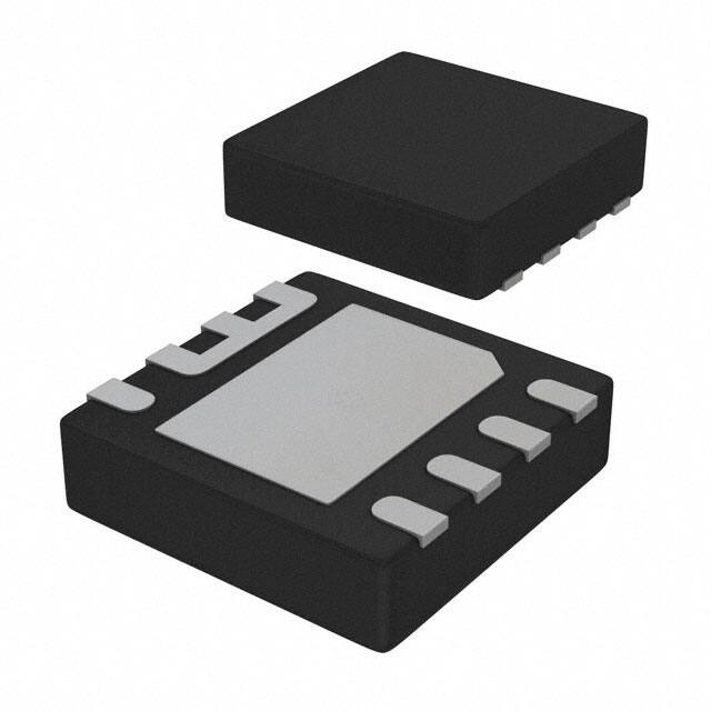
TPS22962 采用小型 3mm x 3mm 超薄小外形尺寸无
引线 (WSON)-8 封装 (DNY)。 DNY 封装集成有一个
散热焊盘,此散热焊盘可在高电流和高温应用中实现高
功率耗散。 器件在自然通风环境下的额定运行温度范
围为 -40°C 至 85°C。
器件信息(1)
产品型号
封装
TPS22962
封装尺寸(标称值)
WSON (8)
3.00mm x 3.00mm
(1) 如需了解所有可用封装,请见数据表末尾的可订购产品附录。
4 简化电路原理图
VBIAS
(2.5 V to 5.5 V)
VIN
Power
Supply
RON 与 VIN 之间的关系 (VBIAS = 5V,
,IOUT = -200mA)
6
VOUT
Load
5.5
CL
CIN
ON
TPS22962
RON (m
)
OFF
5
GND
ON
4.5
4
3.5
-40C
3
25C
2.5
85C
2
0.8
1.2
1.6
2
2.4
2.8
3.2
3.6
4
4.4
4.8
VIN (V)
DG007
1
PRODUCTION DATA information is current as of publication date. Products conform to specifications per the terms of the Texas
Instruments standard warranty. Production processing does not necessarily include testing of all parameters.
English Data Sheet: SLVSCN3
�TPS22962
ZHCSCL1A – JUNE 2014 – REVISED JUNE 2014
www.ti.com.cn
目录
1
2
3
4
5
6
7
8
特性 ..........................................................................
应用范围...................................................................
说明 ..........................................................................
简化电路原理图 ........................................................
修订历史记录 ...........................................................
Pin Configuration and Functions .........................
Specifications.........................................................
1
1
1
1
2
3
3
7.1
7.2
7.3
7.4
7.5
7.6
7.7
7.8
3
4
4
4
5
6
7
9
Absolute Maximum Ratings ......................................
Handling Ratings.......................................................
Recommended Operating Conditions.......................
Thermal Information ..................................................
Electrical Characteristics, VBIAS = 5.0 V ...................
Electrical Characteristics, VBIAS = 2.5 V ...................
Switching Characteristics ..........................................
Typical Characteristics ..............................................
Detailed Description ............................................ 14
8.1
8.2
8.3
8.4
9
Overview .................................................................
Functional Block Diagram .......................................
Feature Description.................................................
Device Functional Modes........................................
14
14
14
15
Applications and Implementation ...................... 16
9.1 Application Information............................................ 16
9.2 Typical Application .................................................. 16
10 Power Supply Recommendations ..................... 19
11 Layout................................................................... 19
11.1 Layout Guidelines ................................................. 19
11.2 Layout Example .................................................... 20
12 器件和文档支持 ..................................................... 21
12.1 Trademarks ........................................................... 21
12.2 Electrostatic Discharge Caution ............................ 21
12.3 术语表 ................................................................... 21
13 机械封装和可订购信息 .......................................... 21
5 修订历史记录
Changes from Original (June 2014) to Revision A
Page
•
完整版的最初发布版本。 ....................................................................................................................................................... 1
2
Copyright © 2014, Texas Instruments Incorporated
�TPS22962
www.ti.com.cn
ZHCSCL1A – JUNE 2014 – REVISED JUNE 2014
6 Pin Configuration and Functions
WSON (DNY) PACKAGE
8 PIN
VIN
1
VIN
2
VIN
8
VOUT
VOUT
8
7
VOUT
VOUT
7
(Exposed thermal
VBIAS
3
ON
4
pad)
VIN
1
VIN
2
VIN
3
VBIAS
4
ON
(Exposed thermal
6
VOUT
VOUT
6
5
GND
GND
5
Top View
pad)
Bottom View
Pin Functions
PIN
I/O
DESCRIPTION
NAME
NO.
VIN
1, 2
I
Switch input. Place ceramic bypass capacitor(s) between this pin and GND. See the Detailed
Description section for more information.
VIN
Exposed thermal
Pad
I
Switch input. Place ceramic bypass capacitor(s) between this pin and GND. See the Detailed
Description section for more information.
VBIAS
3
I
Bias voltage. Power supply to the device.
ON
4
I
Active high switch control input. Do not leave floating.
GND
5
–
Ground.
VOUT
6, 7, 8
O
Switch output. Place ceramic bypass capacitor(s) between this pin and GND. See the Detailed
Description section for more information.
7 Specifications
7.1 Absolute Maximum Ratings
Over operating free-air temperature range (unless otherwise noted) (1)
MIN
MAX
VIN
Input voltage range
–0.3
6
V
VBIAS
Bias voltage range
–0.3
6
V
VOUT
Output voltage range
–0.3
6
V
VON
ON pin voltage range
–0.3
6
V
IMAX
Maximum Continuous Switch Current, TA = 70°C
10
A
IPLS
Maximum Pulsed Switch Current, pulse < 300 µs, 2% duty cycle
TJ
Maximum junction temperature
(1)
UNIT
12
A
125
°C
Stresses beyond those listed under Absolute Maximum Ratings may cause permanent damage to the device. These are stress ratings
only, which do not imply functional operation of the device at these or any other conditions beyond those indicated under Recommended
Operating Conditions. Exposure to absolute-maximum-rated conditions for extended periods may affect device reliability.
Copyright © 2014, Texas Instruments Incorporated
3
�TPS22962
ZHCSCL1A – JUNE 2014 – REVISED JUNE 2014
www.ti.com.cn
7.2 Handling Ratings
MIN
Tstg
Storage temperature range
V(ESD)
(1)
(2)
Electrostatic discharge
MAX
UNIT
–65
150
Human body model (HBM), per ANSI/ESDA/JEDEC JS-001, all
pins (1)
0
2
Charged device model (CDM), per JEDEC specification
JESD22-C101, all pins (2)
0
1
°C
kV
JEDEC document JEP155 states that 500-V HBM allows safe manufacturing with a standard ESD control process.
JEDEC document JEP157 states that 250-V CDM allows safe manufacturing with a standard ESD control process.
7.3 Recommended Operating Conditions
Over operating free-air temperature range (unless otherwise noted)
MIN
MAX
UNIT
VIN
Input voltage range
0.8
VBIAS
V
VBIAS
Bias voltage range
2.5
5.5
V
VON
ON voltage range
0
5.5
V
VOUT
Output voltage range
VIN
V
VIH,
V
ON
High-level voltage, ON
VBIAS = 2.5 V to 5.5 V
1.2
5.5
VIL, ON
Low-level voltage, ON
VBIAS = 2.5 V to 5.5 V
0
0.5
V
TA
Operating free-air temperature range
–40
85
°C
CIN
Input Capacitor
1 (1)
(1)
µF
Refer to Detailed Description section.
7.4 Thermal Information
TPS22962
THERMAL METRIC (1)
DNY
8 PINS
RθJA
Junction-to-ambient thermal resistance
44.6
RθJCtop
Junction-to-case (top) thermal resistance
44.4
RθJB
Junction-to-board thermal resistance
17.6
ψJT
Junction-to-top characterization parameter
0.4
ψJB
Junction-to-board characterization parameter
17.4
RθJCbot
Junction-to-case (bottom) thermal resistance
1.1
(1)
4
UNIT
°C/W
For more information about traditional and new thermal metrics, see the IC Package Thermal Metrics application report, SPRA953.
Copyright © 2014, Texas Instruments Incorporated
�TPS22962
www.ti.com.cn
ZHCSCL1A – JUNE 2014 – REVISED JUNE 2014
7.5 Electrical Characteristics, VBIAS = 5.0 V
Unless otherwise noted, the specification in the following table applies over the operating ambient temperature
–40°C ≤ TA ≤ 85°C (Full) and VBIAS = 5.0 V. Typical values are for TA = 25°C (unless otherwise noted).
PARAMETER
TEST CONDITIONS
TA
MIN
TYP
MAX
UNIT
CURRENTS AND THRESHOLDS
IQ, VBIAS
VBIAS quiescent current
IOUT = 0, VIN = VBIAS,
VON = 5.0 V
Full
20.4
26.0
µA
ISD, VBIAS
VBIAS shutdown current
VON = 0 V, VOUT = 0 V
Full
1.1
1.5
µA
VIN = 5.0 V
ISD, VIN
VIN shutdown current
VON = 0 V,
VOUT = 0 V
0.1
VIN = 3.3 V
VIN = 1.8 V
0.1
Full
0.1
VIN = 1.05 V
0.1
VIN = 0.8 V
0.1
ION
ON pin leakage current
VON = 5.5 V
Full
VHYS,
ON pin hysteresis
VBIAS = VIN
25°C
113
25°C
4.4
ON
µA
0.1
µA
mV
RESISTANCE CHARACTERISTICS
VIN = 5.0 V
VIN = 3.3 V
RON
On-state resistance
IOUT = –200 mA,
VBIAS = 5.0 V
VIN = 2.5 V
VIN = 1.8 V
VIN = 1.05 V
VIN = 0.8 V
RPD
Output pulldown resistance
Copyright © 2014, Texas Instruments Incorporated
VIN = 5.0 V, VON = 0 V, VOUT = 1 V
Full
25°C
5.6
4.4
Full
25°C
4.4
4.4
4.4
5.0
5.6
4.4
Full
Full
5.0
5.6
Full
25°C
5.0
5.6
Full
25°C
5.0
5.6
Full
25°C
5.0
5.0
5.6
224
233
mΩ
mΩ
mΩ
mΩ
mΩ
mΩ
Ω
5
�TPS22962
ZHCSCL1A – JUNE 2014 – REVISED JUNE 2014
www.ti.com.cn
7.6 Electrical Characteristics, VBIAS = 2.5 V
Unless otherwise noted, the specification in the following table applies over the operating ambient temperature
–40°C ≤ TA ≤ 85°C (Full) and VBIAS = 2.5 V. Typical values are for TA = 25°C unless otherwise noted.
PARAMETER
TEST CONDITIONS
TA
MIN
TYP
MAX
UNIT
CURRENTS AND THRESHOLDS
IQ, VBIAS
VBIAS quiescent current
IOUT = 0, VIN = VBIAS,
VON = 5.0 V
Full
9.9
12.5
µA
ISD, VBIAS
VBIAS shutdown current
VON = 0 V, VOUT = 0 V
Full
0.5
0.65
µA
ISD, VIN
VIN shutdown current
VON = 0 V,
VOUT = 0 V
ION
ON pin input leakage current
VON = 5.5 V
Full
VHYS,
ON pin hysteresis
VBIAS = VIN
25°C
83
25°C
4.7
VIN = 2.5 V
VIN = 1.8 V
VIN = 1.05 V
0.1
0.1
Full
0.1
VIN = 0.8 V
ON
µA
0.1
0.1
µA
mV
RESISTANCE CHARACTERISTICS
VIN =2.5 V
RON
On-state resistance
IOUT = –200 mA,
VBIAS = 2.5 V
VIN =1.8 V
VIN =1.05 V
VIN = 0.8 V
RPD
6
Output pulldown resistance
VIN = 2.5 V, VON = 0 V, VOUT = 1 V
Full
25°C
6.0
4.6
Full
25°C
4.5
5.1
5.7
4.5
Full
Full
5.2
5.8
Full
25°C
5.3
5.1
5.7
224
233
mΩ
mΩ
mΩ
mΩ
Ω
Copyright © 2014, Texas Instruments Incorporated
�TPS22962
www.ti.com.cn
ZHCSCL1A – JUNE 2014 – REVISED JUNE 2014
7.7 Switching Characteristics
Refer to the timing test circuit in Figure 1 (unless otherwise noted) for references to external components used for the test
condition in the switching characteristics table. Switching characteristics shown below are only valid for the power-up
sequence where VIN and VBIAS are already in steady state condition before the ON pin is asserted high.
PARAMETER
TEST CONDITION
MIN
TYP
MAX
UNIT
VIN = 5 V, VON = VBIAS = 5 V, TA = 25ºC (unless otherwise noted)
tON
Turn-on time
tOFF
Turn-off time
tR
VOUT rise time
tF
VOUT fall time
tD
Delay time
2397
4
RL = 10 Ω, CL = 0.1 µF
2663
µs
2
1009
VIN = 3.3 V, VON = VBIAS = 5 V, TA = 25ºC (unless otherwise noted)
tON
Turn-on time
1811
tOFF
Turn-off time
4
tR
VOUT rise time
tF
VOUT fall time
tD
Delay time
RL = 10 Ω, CL = 0.1 µF
1756
µs
2
897
VIN = 0.8 V, VON = VBIAS = 5 V, TA = 25ºC (unless otherwise noted)
tON
Turn-on time
981
tOFF
Turn-off time
4
tR
VOUT rise time
tF
VOUT fall time
tD
Delay time
RL = 10 Ω, CL = 0.1 µF
500
µs
2
714
VIN = 2.5 V, VON = 5 V, VBIAS = 2.5 V, TA = 25ºC (unless otherwise noted)
tON
Turn-on time
tOFF
Turn-off time
tR
VOUT rise time
tF
VOUT fall time
tD
Delay time
1576
8
RL = 10Ω, CL = 0.1 µF
1372
µs
2
865
VIN = 1.8V, VON = 5 V, VBIAS = 2.5 V, TA = 25ºC (unless otherwise noted)
tON
Turn-on time
tOFF
Turn-off time
tR
VOUT rise time
tF
VOUT fall time
tD
Delay time
1343
7
RL = 10 Ω, CL = 0.1 µF
1006
µs
2
815
VIN = 0.8 V, VON = 5V, VBIAS = 2.5 V, TA = 25ºC (unless otherwise noted)
tON
Turn-on time
tOFF
Turn-off time
tR
VOUT rise time
tF
VOUT fall time
tD
Delay time
Copyright © 2014, Texas Instruments Incorporated
994
8
RL = 10 Ω, CL = 0.1 µF
502
µs
2
723
7
�TPS22962
ZHCSCL1A – JUNE 2014 – REVISED JUNE 2014
www.ti.com.cn
VIN
VOUT
CIN = 1µF
CL
+
-
ON
(A)
RL
ON
GND
TPS22962
OFF
GND
GND
(1)
Rise and fall times of the control signal is 100ns.
Figure 1. Test Circuit
VON
50%
50%
t OFF
t ON
VOUT
50%
50%
tF
tR
90%
VOUT
10%
10%
90%
10%
tD
Figure 2. Timing Waveforms
8
Copyright © 2014, Texas Instruments Incorporated
�TPS22962
www.ti.com.cn
ZHCSCL1A – JUNE 2014 – REVISED JUNE 2014
7.8 Typical Characteristics
25
1.6
1.4
20
ISD,VBIAS (�A)
IQ,VBIAS (�A)
1.2
15
10
-40C
5
1
0.8
0.6
-40C
0.4
25C
25C
0.2
85C
85C
0
0
2.5
3
3.5
4
4.5
5
5.5
VBIAS (V)
VIN = VBIAS
2.5
3
VON = 5 V
4
4.5
5
5.5
VBIAS (V)
IOUT = 0 A
VIN = VBIAS
Figure 3. IQ,VBIAS vs VBIAS
DG002
VON = 0 V
VOUT = 0 V
Figure 4. ISD,VBIAS vs VBIAS
0.03
6.0
0.025
5.5
0.02
5.0
RON (m
�
ISD,VIN (�A)
3.5
DG001
0.015
4.5
4.0
0.01
-40C
0.005
3.5
25C
85C
3.0
0
0.8
1.2
1.6
2
2.4
2.8
3.2
3.6
4
4.4
VIN (V)
VBIAS = 5 V
±40
4.8
VIN = 1.05V
VIN =1.2V
VIN =1.5V
VIN =1.8V
VIN =2.5V
10
±15
35
60
85
110
Junction Temperature (C)
DG003_5V
VON = 0 V
VIN = 0.8V
VOUT = 0 V
VBIAS = 2.5 V
Figure 5. ISD,VIN vs VIN
VON = 5 V
C006
IOUT = –200 mA
Figure 6. RON vs Junction Temperature
6.0
6
5.5
5.5
5
RON (m
)
RON (m
�
5.0
4.5
4.0
VIN = 0.8V
VIN = 1.2V
VIN = 2.5V
VIN = 4.2V
3.5
3.0
±40
±15
10
35
60
85
VBIAS = 5 V
VON = 5 V
3.5
-40C
25C
2.5
85C
2
110
0.8
1
IOUT = –200 mA
1.2
1.4
1.6
1.8
VIN (V)
C006
Figure 7. RON vs Junction Temperature
Copyright © 2014, Texas Instruments Incorporated
4
3
VIN = 1.05V
VIN = 1.8V
VIN = 3.3V
VIN =5V
Junction Temperature (C)
4.5
VBIAS = 2.5 V
VON = 5 V
2
2.2
2.4
DG006
IOUT = –200 mA
Figure 8. RON vs VIN
9
�TPS22962
ZHCSCL1A – JUNE 2014 – REVISED JUNE 2014
www.ti.com.cn
6
6
5.5
5.5
5
5
4.5
4.5
4
3.5
-40C
3
RON (m
)
RON (m
)
Typical Characteristics (continued)
4
3.5
3
25C
2.5
VBIAS = 2.5V
2.5
85C
2
VBIAS = 5V
2
0.8
1.2
1.6
2
2.4
2.8
3.2
3.6
4
4.4
4.8
VIN (V)
VBIAS = 5 V
0.8
1.2
1.6
2
2.4
VON = 5 V
2.8
3.2
3.6
4
4.4
4.8
VIN (V)
DG007
IOUT = –200 mA
TA = 25°C
DG012
VON = 5 V
Figure 9. RON vs VIN
IOUT = –200 mA
Figure 10. RON vs VIN
7
240
235
6
225
RON (m
�
RPD (
)
230
220
215
4
-40°C
-40C
210
5
3
25°C
25C
205
85°C
85C
2
200
0.8
2.5 2.75 3 3.25 3.5 3.75 4 4.25 4.5 4.75 5 5.25 5.5
VBIAS (V)
VON = 0 V
1.0
1.4
DG016
VIN = 1.05 V
1.6
1.8
2.0
2.2
2.4
VIN (V)
VBIAS = 2.5 V
VOUT = 1 V
C002
VON = 5 V
IOUT = –10 A
Figure 12. RON vs VIN at 10A load
Figure 11. RPD vs VBIAS
6.0
7.0
5.5
6.5
5.0
VIN = 0.8V
VIN = 1.05V
VIN =1.2V
VIN =1.5V
VIN =1.8V
VIN =2.5V
6.0
RON (m
�
RON (m
)
1.2
4.5
4.0
5.5
5.0
3.5
-40°C
3.0
25°C
4.5
85°C
2.5
4.0
0.8
1.2
1.6
2.0
2.4
2.8
3.2
3.6
4.0
VIN (V)
VBIAS = 5 V
VON = 5 V
Figure 13. RON vs VIN at 10A load
10
4.4
4.8
1
2
4
5
6
7
IOUT (A)
C001
IOUT = –10 A
3
VBIAS = 2.5 V
VON = 5 V
8
9
10
C002
TA = 25°C
Figure 14. RON vs IOUT
Copyright © 2014, Texas Instruments Incorporated
�TPS22962
www.ti.com.cn
ZHCSCL1A – JUNE 2014 – REVISED JUNE 2014
Typical Characteristics (continued)
6.5
VIN = 0.8V
VIN = 1.2V
VIN = 1.8V
VIN = 3.3V
VIN =5V
6.0
0.12
0.1
VHYS (V)
RON (m
)
5.5
0.14
VIN = 1.05V
VIN = 1.5V
VIN = 2.5V
VIN = 4.2V
5.0
4.5
4.0
3.5
0.08
0.06
0.04
-40C
0.02
25C
85C
3.0
1
2
3
4
5
6
7
8
9
IOUT (A)
VBIAS = 5 V
0
10
2.5 2.75 3 3.25 3.5 3.75 4 4.25 4.5 4.75 5 5.25 5.5
VBIAS (V)
C001
VON = 5 V
TA = 25°C
VIN = VBIAS
Figure 15. RON vs IOUT
Figure 16. VHYS vs VBIAS
1.2
1.2
1.1
1.1
1
1
VIH,ON (V)
VIL,ON (V)
DG017HYS
0.9
0.8
0.7
-40C
0.6
25C
0.9
0.8
0.7
-40C
0.6
25C
85C
85C
0.5
0.5
2.5 2.75 3 3.25 3.5 3.75 4 4.25 4.5 4.75 5 5.25 5.5
VBIAS (V)
VIN = VBIAS
2.5 2.75 3 3.25 3.5 3.75 4 4.25 4.5 4.75 5 5.25 5.5
VBIAS (V)
DG098
IOUT = 0 A
VIN = VBIAS
Figure 17. VIL,ON vs VBIAS
DG017H
IOUT = 0 A
Figure 18. VIH,ON vs VBIAS
1000
1200
1100
900
1000
900
tD (
s)
tD (
s)
800
700
800
700
600
-40C
500
25C
-40C
600
25C
500
85C
85C
400
400
0.8
1.05
1.3
1.55
1.8
VIN (V)
VBIAS = 2.5 V
RL = 10 Ω
Figure 19. tD vs VIN
Copyright © 2014, Texas Instruments Incorporated
2.05
2.3
0.8
1.2
1.6
CL = 0.1 µF
2
2.4
2.8
3.2
3.6
VIN (V)
DG018
VBIAS = 5 V
RL = 10 Ω
4
4.4
4.8
DG019
CL = 0.1 µF
Figure 20. tD vs VIN
11
�TPS22962
ZHCSCL1A – JUNE 2014 – REVISED JUNE 2014
www.ti.com.cn
4
4
3
3
tF (
s)
tF (
s)
Typical Characteristics (continued)
2
-40C
1
2
-40C
1
25C
25C
85C
85C
0
0
0.8
1.05
1.3
1.55
1.8
2.05
2.3
VIN (V)
RL = 10 Ω
VBIAS = 2.5 V
0.8
1.2
1.6
2
2.4
2.8
3.2
3.6
4
4.4
4.8
VIN (V)
DG020
CL = 0.1 µF
RL = 10 Ω
VBIAS = 5 V
Figure 21. tF vs VIN
DG021
CL = 0.1 µF
Figure 22. tF vs VIN
12
6
11
5
9
tOFF (
s)
tOFF (
s)
10
8
7
-40C
6
4
-40C
3
25C
5
25C
85C
85C
4
2
0.8
1.05
1.3
1.55
1.8
2.05
2.3
VIN (V)
1.2
1.6
2
2.4
2.8
3.2
3.6
4
4.4
4.8
VIN (V)
DG022
RL = 10 Ω
VBIAS = 2.5 V
0.8
CL = 0.1 µF
Figure 23. tOFF vs VIN
DG024
RL = 10 Ω
VBIAS = 5 V
CL = 0.1 µF
Figure 24. tOFF vs VIN
1800
3000
1600
2500
tON (
s)
tON (
s)
1400
1200
2000
1500
1000
-40C
800
-40C
1000
25C
25C
85C
85C
600
500
0.8
1.05
1.3
1.55
1.8
VIN (V)
VBIAS = 2.5 V
RL = 10 Ω
Figure 25. tON vs VIN
12
2.05
2.3
0.8
1.2
1.6
CL = 0.1 µF
2
2.4
2.8
3.2
3.6
VIN (V)
DG025
VBIAS = 5 V
RL = 10 Ω
4
4.4
4.8
DG026
CL = 0.1 µF
Figure 26. tON vs VIN
Copyright © 2014, Texas Instruments Incorporated
�TPS22962
www.ti.com.cn
ZHCSCL1A – JUNE 2014 – REVISED JUNE 2014
1600
3000
1400
2500
1200
2000
tR (
s)
tR (
s)
Typical Characteristics (continued)
1000
800
1500
1000
-40C
600
-40C
500
25C
25C
85C
85C
400
0
0.8
1.05
1.3
1.55
1.8
2.05
2.3
VIN (V)
RL = 10 Ω
VBIAS = 2.5 V
0.8
CL = 0.1 µF
3750
3000
3250
2750
2750
2250
tR (
s)
tR (
s)
2500
2000
1750
VBIAS = 2.5V
VBIAS = 3.3V
VBIAS = 3.6V
VBIAS = 4.2V
VBIAS = 5.0V
VBIAS = 5.5V
1500
1250
1000
750
500
4
RL = 10 Ω
3.2
3.6
4
4.4
4.8
DG028
RL = 10 Ω
VIN = 0.8V
VIN =1.2V
VIN =1.8V
VIN =3.3V
VIN =4.2V
CL = 0.1 µF
CL = 0.1 µF
VIN = 1.05V
VIN =1.5V
VIN =2.5V
VIN =3.6V
VIN =5.0V
1750
1250
750
250
2.5 2.75 3 3.25 3.5 3.75 4 4.25 4.5 4.75 5 5.25 5.5
VBIAS (V)
DG023
Figure 29. tR vs VIN for Various VBIAS
Copyright © 2014, Texas Instruments Incorporated
2.8
2250
4.4 4.8 5.2
VIN (V)
TA = 25°C
2.4
Figure 28. tR vs VIN
3250
2.4 2.8 3.2 3.6
2
VBIAS = 5 V
3500
2
1.6
VIN (V)
Figure 27. tR vs VIN
0.8 1.2 1.6
1.2
DG027
TA = 25°C
RL = 10 Ω
DG030
CL = 0.1 µF
Figure 30. tR vs VBIAS for Various VIN
13
�TPS22962
ZHCSCL1A – JUNE 2014 – REVISED JUNE 2014
www.ti.com.cn
8 Detailed Description
8.1 Overview
The device is a 5.5 V, 10 A load switch in a 8-pin SON package. To reduce voltage drop for low voltage and high
current rails, the device implements an ultra-low resistance N-channel MOSFET which reduces the drop out
voltage through the device.
The device has a controlled and fixed slew rate which helps reduce or eliminate power supply droop due to large
inrush currents. During shutdown, the device has very low leakage currents, thereby reducing unnecessary
leakages for downstream modules during standby. Integrated control logic, driver, charge pump, and output
discharge FET eliminates the need for any external components, which reduces solution size and bill of materials
(BOM) count.
8.2 Functional Block Diagram
VIN
Charge
Pump
VBIAS
ON
Control
Logic
Driver
VOUT
GND
8.3 Feature Description
8.3.1 On/off Control
The ON pin controls the state of the load switch, and asserting the pin high (active high) enables the switch. The
ON pin is compatible with standard GPIO logic threshold and can be used with any microcontroller or discrete
logic with 1.2-V or higher GPIO voltage. This pin cannot be left floating and must be tied either high or low for
proper functionality.
14
Copyright © 2014, Texas Instruments Incorporated
�TPS22962
www.ti.com.cn
ZHCSCL1A – JUNE 2014 – REVISED JUNE 2014
Feature Description (continued)
8.3.2
Input Capacitor (CIN)
To limit the voltage drop on the input supply caused by transient in-rush currents when the switch turns on into a
discharged load capacitor or short-circuit, a capacitor needs to be placed between VIN and GND. A 1-µF ceramic
capacitor, CIN, placed close to the pins, is usually sufficient. Higher values of CIN can be used to further reduce
the voltage drop in high-current application. When switching heavy loads, it is recommended to have an input
capacitor 10 times higher than the output capacitor to avoid excessive voltage drop; however, a 10 to 1 ratio for
capacitance is not required for proper functionality of the device, but a ratio smaller than 10 to 1 (such as 1 to 1)
could cause a VIN dip upon turn-on due to inrush currents based on external factor such as board parasitics and
output bulk capacitance.
8.3.3 Output Capacitor (CL)
Due to the integrated body diode in the N-channel MOSFET, a CIN greater than CL is highly recommended. A CL
greater than CIN can cause VOUT to exceed VIN when the system supply is removed. This could result in current
flow through the body diode from VOUT to VIN. A CIN to CL ratio of 10 to 1 is recommended for minimizing VIN
dip caused by inrush currents during startup, however a 10 to 1 ratio for capacitance is not required for proper
functionality of the device. A ratio smaller than 10 to 1 (such as 1 to 1) could cause a VIN dip upon turn-on due to
inrush currents based on external factor such as board parasitics and output bulk capacitance.
8.3.4 VIN and VBIAS Voltage Range
For optimal RON performance, make sure VIN ≤ VBIAS. The device may still be functional if VIN > VBIAS but it will
exhibit RON greater than what is listed in the Electrical Characteristics table. See Figure 31 for an example of a
typical device. Notice the increasing RON as VIN increases. Be sure to never exceed the maximum voltage rating
for VIN and VBIAS. Performance of the device is not guaranteed for VIN > VBIAS.
10
9
RON (m
)
8
VBIAS = 2.5V
VBIAS = 3.0V
VBIAS = 3.3V
VBIAS = 3.6V
VBIAS = 4.2V
VBIAS =5.0V
VBIAS =5.5V
7
6
5
4
3
0.8 1.2 1.6
2
2.4 2.8 3.2 3.6
4
4.4 4.8 5.2
VIN (V)
DG055
Figure 31. RON vs VIN (VIN > VBIAS)
8.4 Device Functional Modes
Table 1 shows the connection of VOUT depending on the state of the ON pin.
Table 1. VOUT Connection
ON
VOUT
L
GND
H
VIN
Copyright © 2014, Texas Instruments Incorporated
15
�TPS22962
ZHCSCL1A – JUNE 2014 – REVISED JUNE 2014
www.ti.com.cn
9 Applications and Implementation
9.1 Application Information
This section will highlight some of the design considerations when implementing this device in various
applications. A PSPICE model for this device is also available in the product page of this device on www.ti.com
for further aid.
9.2 Typical Application
This application demonstrates how the TPS22962 can be used to power downstream modules with large
capacitances. The example below is powering a 100-µF capacitive output load.
VIN
VIN
VIN
(exposed
pad)
CIN
ON
ON
VOUT
VOUT
VBIAS
VBIAS
CL = 100µF
GND
Figure 32. Typical Application Schematic for Powering a Downstream Module
9.2.1 Design Requirements
For this design example, use the following as the input parameters.
Table 2. Design Parameters
DESIGN PARAMETER
EXAMPLE VALUE
VIN
5.0 V
VBIAS
5.0 V
Load current
10 A
9.2.2 Detailed Design Procedure
To
•
•
•
begin the design process, the designer needs to know the following:
VIN voltage
VBIAS voltage
Load current
9.2.2.1
VIN to VOUT Voltage Drop
The VIN to VOUT voltage drop in the device is determined by the RON of the device and the load current. The
RON of the device depends upon the VIN and VBIAS conditions of the device. Refer to the RON specification of the
device in the Electrical Characteristics table of this datasheet. Once the RON of the device is determined based
upon the VIN and VBIAS conditions, use Equation 1 to calculate the VIN to VOUT voltage drop:
DV = ILOAD ´ RON
(1)
where
• ΔV = voltage drop from VIN to VOUT
• ILOAD = load current
• RON = On-resistance of the device for a specific VIN and VBIAS combination
An appropriate ILOAD must be chosen such that the IMAX specification of the device is not violated.
16
Copyright © 2014, Texas Instruments Incorporated
�TPS22962
www.ti.com.cn
ZHCSCL1A – JUNE 2014 – REVISED JUNE 2014
9.2.2.2 Inrush Current
To determine how much inrush current will be caused by the CL capacitor, use Equation 2:
dV
IINRUSH = CL ´ OUT
dt
(2)
where
• IINRUSH = amount of inrush caused by CL
• CL = capacitance on VOUT
• dt = time it takes for change in VOUT during the ramp up of VOUT when the device is enabled
• dVOUT = change in VOUT during the ramp up of VOUT when the device is enabled
An appropriate CL value should be placed on VOUT such that the IMAX and IPLS specficiations of the device are
not violated.
Figure 33. Inrush Current (VBIAS = 5 V, VIN = 5 V, CL = 100 µF)
9.2.2.3 Thermal Considerations
The maximum IC junction temperature should be restricted to 125°C under normal operating conditions. To
calculate the maximum allowable dissipation, PD(max) for a given output current and ambient temperature, use
Equation 3.
PD(MAX) =
TJ(MAX) - TA
θJA
(3)
where
• PD(max) = maximum allowable power dissipation
• TJ(max) = maximum allowable junction temperature (125°C for the TPS22962)
• TA = ambient temperature of the device
• θJA = junction to air thermal impedance. See Thermal Information section. This parameter is highly
dependent upon board layout.
Copyright © 2014, Texas Instruments Incorporated
17
�TPS22962
ZHCSCL1A – JUNE 2014 – REVISED JUNE 2014
www.ti.com.cn
9.2.3 Application Curves
VBIAS = 5 V
CL = 0.1 µF
VIN = 5 V
CIN = 1 µF
VBIAS = 5 V
CL = 0.1 µF
VIN = 1.05 V
Figure 34. tR at VBIAS = 5 V
VBIAS = 2.5 V
CL = 0.1 µF
VIN = 2.5 V
Figure 35. tR at VBIAS = 5 V
CIN = 1 µF
Figure 36. tR at VBIAS = 2.5 V
VBIAS = 5 V
CL = 0.1 µF
VIN = 5 V
Figure 38. tF at VBIAS = 5 V
18
CIN = 1 µF
VBIAS = 2.5 V
CL = 0.1 µF
VIN = 1.05 V
CIN = 1 µF
Figure 37. tR at VBIAS = 2.5 V
CIN = 1 µF
VBIAS = 5 V
CL = 0.1 µF
VIN = 2.5 V
CIN = 1 µF
Figure 39. tF at VBIAS = 5 V
Copyright © 2014, Texas Instruments Incorporated
�TPS22962
www.ti.com.cn
VBIAS = 2.5 V
CL = 0.1 µF
ZHCSCL1A – JUNE 2014 – REVISED JUNE 2014
VIN = 2.5 V
CIN = 1 µF
Figure 40. tF at VBIAS = 2.5 V
VBIAS = 2.5 V
CL = 0.1 µF
VIN = 0.8 V
CIN = 1 µF
Figure 41. tF at VBIAS = 2.5 V
10 Power Supply Recommendations
The device is designed to operate from a VBIAS range of 2.5 V to 5.5 V and VIN range of 0.8 V to 5.5 V. This
supply must be well regulated and placed as close to the device pin as possible with the recommended 1µF
bypass capacitor. If the supply is located more than a few inches from the device pins, additional bulk
capacitance may be required in addition to the ceramic bypass capacitors. If additional bulk capacitance is
required, an electrolytic, tantalum, or ceramic capacitor of 10 µF may be sufficient.
11 Layout
11.1 Layout Guidelines
•
•
•
•
•
VIN and VOUT traces should be as short and wide as possible to accommodate for high current.
Use vias under the exposed thermal pad for thermal relief for high current operation.
The VIN pin should be bypassed to ground with low ESR ceramic bypass capacitors. The typical
recommended bypass capacitance is 1-µF ceramic with X5R or X7R dielectric. This capacitor should be
placed as close to the device pins as possible.
The VOUT pin should be bypassed to ground with low ESR ceramic bypass capacitors. The typical
recommended bypass capacitance is one-tenth of the VIN bypass capacitor of X5R or X7R dielectric rating.
This capacitor should be placed as close to the device pins as possible.
The VBIAS pin should be bypassed to ground with low ESR ceramic bypass capacitors. The typical
recommended bypass capacitance is 0.1-µF ceramic with X5R or X7R dielectric.
Copyright © 2014, Texas Instruments Incorporated
19
�TPS22962
ZHCSCL1A – JUNE 2014 – REVISED JUNE 2014
www.ti.com.cn
11.2 Layout Example
VIA to Power Ground Plane
VIA to VIN Plane
VIN
VOUT
VIN Bypass
Capacitor
VIN
VIN
To Bias Supply
VOUT Bypass
Capacitor
VBIAS
GND
ON
To GPIO
control
Exposed Thermal
Pad Area
Figure 42. Recommended Board Layout
20
Copyright © 2014, Texas Instruments Incorporated
�TPS22962
www.ti.com.cn
ZHCSCL1A – JUNE 2014 – REVISED JUNE 2014
12 器件和文档支持
12.1 Trademarks
All trademarks are the property of their respective owners.
12.2 Electrostatic Discharge Caution
These devices have limited built-in ESD protection. The leads should be shorted together or the device placed in conductive foam
during storage or handling to prevent electrostatic damage to the MOS gates.
12.3 术语表
SLYZ022 — TI 术语表。
这份术语表列出并解释术语、首字母缩略词和定义。
13 机械封装和可订购信息
以下页中包括机械封装和可订购信息。 这些信息是针对指定器件可提供的最新数据。 这些数据会在无通知且不对
本文档进行修订的情况下发生改变。 欲获得该数据表的浏览器版本,请查阅左侧的导航栏。
Copyright © 2014, Texas Instruments Incorporated
21
�PACKAGE OPTION ADDENDUM
www.ti.com
30-Jun-2025
PACKAGING INFORMATION
Orderable part number
(1)
Status
Material type
(1)
(2)
Package | Pins
Package qty | Carrier
RoHS
(3)
Lead finish/
Ball material
MSL rating/
Peak reflow
(4)
(5)
Op temp (°C)
Part marking
(6)
TPS22962DNYR
Active
Production
WSON (DNY) | 8
3000 | LARGE T&R
Yes
Call TI | Nipdau
| Nipdau
Level-2-260C-1 YEAR
-40 to 85
962A0
TPS22962DNYR.B
Active
Production
WSON (DNY) | 8
3000 | LARGE T&R
Yes
NIPDAU
Level-2-260C-1 YEAR
-40 to 105
962A0
TPS22962DNYRG4
Active
Production
WSON (DNY) | 8
3000 | LARGE T&R
Yes
NIPDAU
Level-2-260C-1 YEAR
-40 to 105
962A0
TPS22962DNYRG4.B
Active
Production
WSON (DNY) | 8
3000 | LARGE T&R
Yes
NIPDAU
Level-2-260C-1 YEAR
-40 to 105
962A0
TPS22962DNYT
Active
Production
WSON (DNY) | 8
250 | SMALL T&R
Yes
Call TI | Nipdau
Level-2-260C-1 YEAR
-40 to 85
962A0
TPS22962DNYT.B
Active
Production
WSON (DNY) | 8
250 | SMALL T&R
Yes
NIPDAU
Level-2-260C-1 YEAR
-40 to 105
962A0
Status: For more details on status, see our product life cycle.
(2)
Material type: When designated, preproduction parts are prototypes/experimental devices, and are not yet approved or released for full production. Testing and final process, including without limitation quality assurance,
reliability performance testing, and/or process qualification, may not yet be complete, and this item is subject to further changes or possible discontinuation. If available for ordering, purchases will be subject to an additional
waiver at checkout, and are intended for early internal evaluation purposes only. These items are sold without warranties of any kind.
(3)
RoHS values: Yes, No, RoHS Exempt. See the TI RoHS Statement for additional information and value definition.
(4)
Lead finish/Ball material: Parts may have multiple material finish options. Finish options are separated by a vertical ruled line. Lead finish/Ball material values may wrap to two lines if the finish value exceeds the maximum
column width.
(5)
MSL rating/Peak reflow: The moisture sensitivity level ratings and peak solder (reflow) temperatures. In the event that a part has multiple moisture sensitivity ratings, only the lowest level per JEDEC standards is shown.
Refer to the shipping label for the actual reflow temperature that will be used to mount the part to the printed circuit board.
(6)
Part marking: There may be an additional marking, which relates to the logo, the lot trace code information, or the environmental category of the part.
Multiple part markings will be inside parentheses. Only one part marking contained in parentheses and separated by a "~" will appear on a part. If a line is indented then it is a continuation of the previous line and the two
combined represent the entire part marking for that device.
Important Information and Disclaimer:The information provided on this page represents TI's knowledge and belief as of the date that it is provided. TI bases its knowledge and belief on information provided by third parties, and
makes no representation or warranty as to the accuracy of such information. Efforts are underway to better integrate information from third parties. TI has taken and continues to take reasonable steps to provide representative
and accurate information but may not have conducted destructive testing or chemical analysis on incoming materials and chemicals. TI and TI suppliers consider certain information to be proprietary, and thus CAS numbers
and other limited information may not be available for release.
In no event shall TI's liability arising out of such information exceed the total purchase price of the TI part(s) at issue in this document sold by TI to Customer on an annual basis.
Addendum-Page 1
�PACKAGE OPTION ADDENDUM
www.ti.com
30-Jun-2025
Addendum-Page 2
�PACKAGE MATERIALS INFORMATION
www.ti.com
18-Jun-2025
TAPE AND REEL INFORMATION
REEL DIMENSIONS
TAPE DIMENSIONS
K0
P1
B0 W
Reel
Diameter
Cavity
A0
B0
K0
W
P1
A0
Dimension designed to accommodate the component width
Dimension designed to accommodate the component length
Dimension designed to accommodate the component thickness
Overall width of the carrier tape
Pitch between successive cavity centers
Reel Width (W1)
QUADRANT ASSIGNMENTS FOR PIN 1 ORIENTATION IN TAPE
Sprocket Holes
Q1
Q2
Q1
Q2
Q3
Q4
Q3
Q4
User Direction of Feed
Pocket Quadrants
*All dimensions are nominal
Device
TPS22962DNYRG4
Package Package Pins
Type Drawing
WSON
DNY
8
SPQ
Reel
Reel
A0
Diameter Width (mm)
(mm) W1 (mm)
3000
330.0
12.4
Pack Materials-Page 1
3.3
B0
(mm)
K0
(mm)
P1
(mm)
3.3
1.0
8.0
W
Pin1
(mm) Quadrant
12.0
Q2
�PACKAGE MATERIALS INFORMATION
www.ti.com
18-Jun-2025
TAPE AND REEL BOX DIMENSIONS
Width (mm)
W
L
H
*All dimensions are nominal
Device
Package Type
Package Drawing
Pins
SPQ
Length (mm)
Width (mm)
Height (mm)
TPS22962DNYRG4
WSON
DNY
8
3000
367.0
367.0
38.0
Pack Materials-Page 2
�PACKAGE OUTLINE
WSON - 0.8 mm max height
DNY0008A
PLASTIC QUAD FLATPACK- NO LEAD
3.15
2.85
B
A
PIN 1 INDEX AREA
3.15
2.85
C
0.8
0.7
SEATING PLANE
0.08 C
0.05
0.00
1.6±0.1
SYMM
EXPOSED THERMAL
PAD
5X 0.5
0.3
(0.2) TYP
6X 0.65
4
2.4±0.1
5
SYMM
2X
1.95
8X 0.35
0.25
8
1
PIN1 ID
(OPTIONAL)
0.1
0.05
C A B
C
2X (0.2)
0.5
0.3
4221022/E 06/2020
NOTES:
1.
2.
3.
All linear dimensions are in millimeters. Any dimensions in parenthesis are for reference only. Dimensioning and tolerancing
per ASME Y14.5M.
This drawing is subject to change without notice.
The package thermal pad must be soldered to the printed circuit board for optimal thermal and mechanical performance.
www.ti.com
�EXAMPLE BOARD LAYOUT
WSON - 0.8 mm max height
DNY0008A
PLASTIC QUAD FLATPACK- NO LEAD
(1.6)
5X (0.6)
SYMM
(0.6)
5X (0.3)
1
8
3X (0.65)
(0.325)
SYMM
(0.95)
(1.6)
(2.4)
(0.975)
4
5
(R0.05) TYP
(0.55)
(Ø0.2) VIA
TYP
(2.8)
LAND PATTERN EXAMPLE
SCALE: 20X
0.07 MAX
ALL AROUND
0.07 MIN
ALL AROUND
METAL
EXPOSED METAL
EXPOSED METAL
SOLDER MASK
OPENING
NON- SOLDER MASK
DEFINED
(PREFERRED)
METAL UNDER
SOLDER MASK
SOLDER MASK
OPENING
SOLDER MASK
DEFINED
SOLDER MASK DETAILS
4221022/E 06/2020
NOTES: (continued)
4.
5.
This package is designed to be soldered to a thermal pad on the board. For more information, see Texas Instruments literature
number SLUA271 (www.ti.com/lit/slua271) .
Vias are optional depending on application, refer to device data sheet. If any vias are implemented, refer to their locations shown
on this view. It is recommended that vias under paste be filled, plugged or tented.
www.ti.com
�EXAMPLE STENCIL DESIGN
WSON - 0.8 mm max height
DNY0008A
PLASTIC QUAD FLATPACK- NO LEAD
2X (1.47)
5X (0.6)
SYMM
(0.6)
5X (0.3)
8
1
(0.325)
(1.6)
(0.63)
SYMM
2X
(1.06) 3X (0.65)
(0.975)
4
METAL
TYP
5
(R0.05) TYP
(2.8)
SOLDER PASTE EXAMPLE
BASED ON 0.125 mm THICK STENCIL
EXPOSED PAD
81% PRINTED COVERAGE BY AREA
SCALE: 20X
4221022/E 06/2020
NOTES: (continued)
6.
Laser cutting apertures with trapezoidal walls and rounded corners may offer better paste release. IPC-7525 may have alternate
design recommendations.
www.ti.com
�重要通知和免责声明
TI“按原样”提供技术和可靠性数据(包括数据表)、设计资源(包括参考设计)、应用或其他设计建议、网络工具、安全信息和其他资源,
不保证没有瑕疵且不做出任何明示或暗示的担保,包括但不限于对适销性、某特定用途方面的适用性或不侵犯任何第三方知识产权的暗示担
保。
这些资源可供使用 TI 产品进行设计的熟练开发人员使用。您将自行承担以下全部责任:(1) 针对您的应用选择合适的 TI 产品,(2) 设计、验
证并测试您的应用,(3) 确保您的应用满足相应标准以及任何其他功能安全、信息安全、监管或其他要求。
这些资源如有变更,恕不另行通知。TI 授权您仅可将这些资源用于研发本资源所述的 TI 产品的相关应用。 严禁以其他方式对这些资源进行
复制或展示。您无权使用任何其他 TI 知识产权或任何第三方知识产权。您应全额赔偿因在这些资源的使用中对 TI 及其代表造成的任何索
赔、损害、成本、损失和债务,TI 对此概不负责。
TI 提供的产品受 TI 的销售条款或 ti.com 上其他适用条款/TI 产品随附的其他适用条款的约束。TI 提供这些资源并不会扩展或以其他方式更改
TI 针对 TI 产品发布的适用的担保或担保免责声明。
TI 反对并拒绝您可能提出的任何其他或不同的条款。IMPORTANT NOTICE
邮寄地址:Texas Instruments, Post Office Box 655303, Dallas, Texas 75265
版权所有 © 2025,德州仪器 (TI) 公司
�