Sample &
Buy
Product
Folder
Support &
Community
Tools &
Software
Technical
Documents
TPS22966
SLVSBH4F – JUNE 2012 – REVISED JULY 2016
TPS22966 5.5-V, 6-A, 16-mΩ On-Resistance Dual-Channel Load Switch
1 Features
3 Description
•
•
•
The TPS22966 is a small, low RON, dual-channel load
switch with controlled turnon. The device contains two
N-channel MOSFETs that can operate over an input
voltage range of 0.8 V to 5.5 V and can support a
maximum continuous current of 6 A per channel.
Each switch is independently controlled by an on and
off input (ON1 and ON2), which can interface directly
with low-voltage control signals. In TPS22966, a 220Ω on-chip load resistor is added for quick-output
discharge when switch is turned off.
1
•
•
•
•
•
•
•
Input Voltage Range: 0.8 V to 5.5 V
Integrated Dual-Channel Load Switch
On-Resistance
– RON = 16 mΩ at VIN = 5 V (VBIAS = 5 V)
– RON = 16 mΩ at VIN = 3.6 V (VBIAS = 5 V)
– RON = 16 mΩ at VIN = 1.8 V (VBIAS = 5 V)
6-A Maximum Continuous Switch Current per
Channel
Low Quiescent Current
– 80 µA (Both Channels)
– 60 µA (Single Channel)
Low Control Input Threshold Enables Use of
1.2-, 1.8-, 2.5-, and 3.3-V Logic
Configurable Rise Time
Quick Output Discharge (QOD) (Optional)
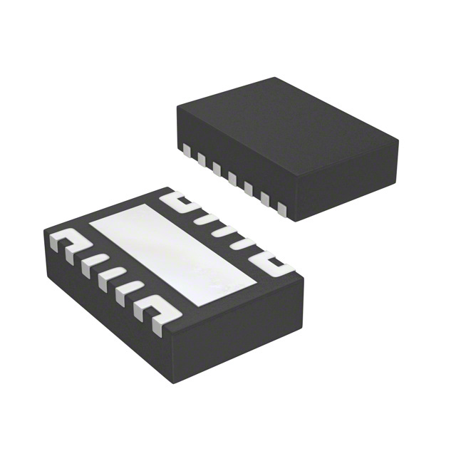
SON 14-Pin Package With Thermal Pad
ESD Performance Tested per JESD 22
– 2-kV HBM and 1-kV CDM
The TPS22966 is available in a small, space-saving
2-mm × 3-mm 14-SON package (DPU) with
integrated thermal pad allowing for high power
dissipation. The device is characterized for operation
over the free-air temperature range of –40°C to
+105°C.
Device Information(1)
PART NUMBER
TPS22966
PACKAGE
WSON (14)
BODY SIZE (NOM)
3.00 mm × 2.00 mm
(1) For all available packages, see the orderable addendum at
the end of the data sheet.
2 Applications
•
•
•
•
•
•
•
Ultrabook™
Notebooks and Netbooks
Tablet PCs
Consumer Electronics
Set-top Boxes and Residental Gateways
Telecom Systems
Solid-State Drives (SSD)
Application Circuit
VIN 1
Dual
Power
Supply
ON
CIN
VOUT1
ON1
CL
RL
CT1
OFF
CT2
or
GND
VBIAS
Dual
DC/DC
converter
VOUT2
VIN2
ON
CIN
ON2
CL
OFF
TPS22966
GND
GND
1
An IMPORTANT NOTICE at the end of this data sheet addresses availability, warranty, changes, use in safety-critical applications,
intellectual property matters and other important disclaimers. PRODUCTION DATA.
�TPS22966
SLVSBH4F – JUNE 2012 – REVISED JULY 2016
www.ti.com
Table of Contents
1
2
3
4
5
6
Features ..................................................................
Applications ...........................................................
Description .............................................................
Revision History.....................................................
Pin Configuration and Functions .........................
Specifications.........................................................
6.1
6.2
6.3
6.4
6.5
6.6
6.7
6.8
6.9
7
8
1
1
1
2
3
4
Absolute Maximum Ratings ...................................... 4
ESD Ratings.............................................................. 4
Recommended Operating Conditions....................... 4
Thermal Information .................................................. 4
Electrical Characteristics—VBIAS = 5 V ..................... 5
Electrical Characteristics—VBIAS = 2.5 V .................. 6
Switching Characteristics .......................................... 7
Typical DC Characteristics........................................ 8
Typical AC Characteristics...................................... 12
Parameter Measurement Information ................ 14
Detailed Description ............................................ 15
8.1 Overview ................................................................. 15
8.2 Functional Block Diagram ....................................... 15
8.3 Feature Description................................................. 16
8.4 Device Functional Modes........................................ 17
9
Application and Implementation ........................ 18
9.1 Application Information............................................ 18
9.2 Typical Application .................................................. 18
10 Power Supply Recommendations ..................... 20
11 Layout................................................................... 20
11.1 Layout Guidelines ................................................. 20
11.2 Layout Example .................................................... 20
11.3 Thermal Considerations ........................................ 20
12 Device and Documentation Support ................. 22
12.1
12.2
12.3
12.4
12.5
Documentation Support ........................................
Receiving Notification of Documentation Updates
Trademarks ...........................................................
Electrostatic Discharge Caution ............................
Glossary ................................................................
22
22
22
22
22
13 Mechanical, Packaging, and Orderable
Information ........................................................... 22
4 Revision History
Changes from Revision E (February 2015) to Revision F
•
Page
Changed (TPS22966 only) to (Optional) in the Features section. ......................................................................................... 1
Changes from Revision D (January 2015) to Revision E
Page
•
Added temperature operating ranges to Electrical Characteristics (VBIAS = 5.0 V) table. ...................................................... 5
•
Added temperature operating ranges to Electrical Characteristics (VBIAS = 2.5 V) table. ...................................................... 6
•
Updated graphics in the Typical Characteristics section........................................................................................................ 8
Changes from Revision C (June 2013) to Revision D
•
Page
Added ESD Ratings table, Feature Description section, Device Functional Modes, Application and Implementation
section, Power Supply Recommendations section, Layout section, Device and Documentation Support section, and
Mechanical, Packaging, and Orderable Information section ................................................................................................. 1
Changes from Revision B (December 2012) to Revision C
Page
•
Added VBIAS to ABSOLUTE MAXIMUM RATINGS table. .................................................................................................... 4
•
Updated SWITCHING CHARACTERISTIC MEASUREMENT INFORMATION. ................................................................... 7
•
Updated Test Circuit Diagram .............................................................................................................................................. 14
•
Updated Functional Block Diagram. .................................................................................................................................... 15
Changes from Revision A (July 2012) to Revision B
•
2
Page
Updated Application Schematic. ............................................................................................................................................ 1
Submit Documentation Feedback
Copyright © 2012–2016, Texas Instruments Incorporated
Product Folder Links: TPS22966
�TPS22966
www.ti.com
SLVSBH4F – JUNE 2012 – REVISED JULY 2016
5 Pin Configuration and Functions
DPU Package
14-Pin WSON
Top View
DPU Package
14-Pin WSON
Bottom View
14
1
14
1
VIN1
VOUT1
VOUT1
VIN1
VIN1
VOUT1
VOUT1
VIN1
CT1
ON1
CT1
ON2
VBIAS
GND
ON2
CT2
VIN2
VIN2
GND
VBIAS
CT2
ON2
VOUT2
VOUT2
VIN2
VOUT2
VOUT2
VIN2
Pin Functions
PIN
NO.
NAME
TYPE
DESCRIPTION
1
VIN1
I
Switch 1 input. Recommended voltage range for this pin for optimal RON performance is 0.8 V to VBIAS.
Place an optional decoupling capacitor between this pin and GND for reduce VIN dip during turnon of
the channel. See the Application Information section for more information
2
VIN1
I
Switch 1 input. Recommended voltage range for this pin for optimal RON performance is 0.8 V to VBIAS.
Place an optional decoupling capacitor between this pin and GND for reduce VIN dip during turnon of
the channel. See the Application Information section for more information
3
ON1
I
Active high switch 1 control input. Do not leave floating
4
VBIAS
I
Bias voltage. Power supply to the device. Recommended voltage range for this pin is 2.5 V to 5.5 V.
See the Application Information section
5
ON2
I
Active high switch 2 control input. Do not leave floating
6
VIN2
I
Switch 2 input. Recommended voltage range for this pin for optimal RON performance is 0.8 V to VBIAS.
Place an optional decoupling capacitor between this pin and GND for reduce VIN dip during turnon of
the channel. See the Application Information section for more information
7
VIN2
I
Switch 2 input. Recommended voltage range for this pin for optimal RON performance is 0.8 V to VBIAS.
Place an optional decoupling capacitor between this pin and GND for reduce VIN dip during turnon of
the channel. See the Application Information section for more information
8
VOUT2
O
Switch 2 output
9
VOUT2
O
Switch 2 output
10
CT2
O
Switch 2 slew rate control. Can be left floating. Capacitor used on this pin mudt be rated for a minimum
of 25 V for desired rise time performance
11
GND
—
Ground
12
CT1
O
Switch 1 slew rate control. Can be left floating. Capacitor used on this pin must be rated for a minimum
of 25 V for desired rise time performance
13
VOUT1
O
Switch 1 output
14
VOUT1
O
Switch 1 output
—
Thermal Pad
—
Thermal pad (exposed center pad) to alleviate thermal stress. Tie to GND. See the Layout section for
layout guidelines
Submit Documentation Feedback
Copyright © 2012–2016, Texas Instruments Incorporated
Product Folder Links: TPS22966
3
�TPS22966
SLVSBH4F – JUNE 2012 – REVISED JULY 2016
www.ti.com
6 Specifications
6.1 Absolute Maximum Ratings
Over operating free-air temperature range (unless otherwise noted) (1)
MIN
MAX
UNIT (2)
VIN1,2
Input voltage
–0.3
6
V
VOUT1,2
Output voltage
–0.3
6
V
VON1,2
ON-pin voltage
–0.3
6
V
VBIAS
VBIAS voltage
–0.3
6
V
IMAX
Maximum continuous switch current per channel
6
A
IPLS
Maximum pulsed switch current per channel, pulse VBIAS but it exhibits RON
greater than what is listed in the Electrical Characteristics table. See Figure 32 for an example of a typical
device. Notice the increasing RON as VIN exceeds VBIAS voltage. Make sure to never exceed the maximum
voltage rating for VIN and VBIAS.
52
On-Resistance (m:)
47
42
VBIAS = 2.5 V
VBIAS = 3.3 V
VBIAS = 3.6 V
VBIAS = 4.2 V
VBIAS = 5 V
VBIAS = 5.5 V
37
32
27
22
17
0.8 1.2 1.6
VIN > VBIAS
2
2.4 2.8 3.2 3.6 4
Input Voltage} (V)
4.4 4.8 5.2 5.6
D050
IOUT= –200 mA
Figure 32. On-Resistance vs Input Voltage
Single Channel
16
Submit Documentation Feedback
Copyright © 2012–2016, Texas Instruments Incorporated
Product Folder Links: TPS22966
�TPS22966
www.ti.com
SLVSBH4F – JUNE 2012 – REVISED JULY 2016
8.4 Device Functional Modes
Table 1 lists the TPS22966 functions.
Table 1. Functions Table
ONx
VINx to VOUTx
VOUTx to GND
L
Off
On
H
On
Off
Submit Documentation Feedback
Copyright © 2012–2016, Texas Instruments Incorporated
Product Folder Links: TPS22966
17
�TPS22966
SLVSBH4F – JUNE 2012 – REVISED JULY 2016
www.ti.com
9 Application and Implementation
NOTE
Information in the following applications sections is not part of the TI component
specification, and TI does not warrant its accuracy or completeness. TI’s customers are
responsible for determining suitability of components for their purposes. Customers should
validate and test their design implementation to confirm system functionality.
9.1 Application Information
This application demonstrates how the TPS22966 can be used to limit inrush current when powering on
downstream modules.
9.2 Typical Application
VIN 1
Dual
Power
Supply
ON
CIN
VOUT1
ON1
CL
RL
CT1
OFF
CT2
or
GND
VBIAS
Dual
DC/DC
converter
VOUT2
VIN2
ON
CIN
ON2
CL
OFF
TPS22966
GND
GND
Figure 33. Typical Application Circuit
9.2.1 Design Requirements
Table 2 shows the TPS22966 desgin parameters.
Table 2. Design Parameters
DESIGN PARAMETER
VALUE
Input voltage
3.3 V
Bias voltage
5V
Load capacitance (CL)
22 µF
Maximum acceptable inrush current
400 mA
9.2.2 Detailed Design Procedure
When the switch is enabled, the output capacitors must be charged up from 0 V to the set value (3.3 V in this
example). This charge arrives in the form of inrush current. Inrush current can be calculated using Equation 1.
Inrush Current = C × dV/dt
where
•
•
•
C is the output capacitance
dV is the output voltage
dt is the rise time
(1)
The TPS22966 offers adjustable rise time for VOUT. This feature allows the user to control the inrush current
during turnon. The appropriate rise time can be calculated using Table 2 and Equation 1 as shown in Equation 2.
400 mA = 22 μF × 3.3 V/dt
dt = 181.5 μs
18
(2)
(3)
Submit Documentation Feedback
Copyright © 2012–2016, Texas Instruments Incorporated
Product Folder Links: TPS22966
�TPS22966
www.ti.com
SLVSBH4F – JUNE 2012 – REVISED JULY 2016
To ensure an inrush current of less than 400 mA, choose a CT value that yields a rise time of more than 181.5
μs. See the oscilloscope captures in the Application Curves section for an example of how the CT capacitor can
be used to reduce inrush current.
9.2.2.1 Adjustable Rise Time
A capacitor to GND on the CTx pins sets the slew rate for each channel. To ensure desired performance, a
capacitor with a minimum voltage rating of 25 V must be used on the CTx pin. An approximate formula for the
relationship between CTx and slew rate is given in Equation 4. Equation 4 accounts for 10% to 90%
measurement on VOUT and does NOT apply for CTx = 0 pF. (Use Table 3 to determine rise times for when CTx =
0 pF).
SR = 0.32 ´ CT + 13.7
where
•
•
•
SR is the slew rate (in µs/V)
CT is the capacitance value on the CTx pin (in pF)
The units for the constant 13.7 is in µs/V.
(4)
Rise time can be calculated by multiplying the input voltage by the slew rate. Table 3 shows rise time values
measured on a typical device. Rise times shown in Table 3 are only valid for the power-up sequence where VIN
and VBIAS are already in steady state condition, and the ON pin is asserted high.
Table 3. Rise Time Values
CTx (pF)
(1)
RISE TIME (µs) 10% - 90%, CL = 0.1µF, CIN = 1µF, RL = 10Ω
(1)
3.3 V
1.8 V
1.5 V
1.2 V
1.05 V
0
124
5V
88
63
60
53
49
0.8 V
42
220
481
323
193
166
143
133
109
470
855
603
348
299
251
228
175
1000
1724
1185
670
570
469
411
342
2200
3328
2240
1308
1088
893
808
650
4700
7459
4950
2820
2429
1920
1748
1411
10000
16059
10835
6040
5055
4230
3770
3033
TYPICAL VALUES at 25°C, VBIAS = 5 V, 25 V X7R 10% CERAMIC CAP.
9.2.3 Application Curves
VBIAS = 5 V
VIN = 3.3 V
CL = 22 μF
Figure 34. Inrush Current with CT = 0 pF
VBIAS = 5 V
VIN = 3.3 V
CL = 22 μF
Figure 35. Inrush Current with CT = 220 pF
Submit Documentation Feedback
Copyright © 2012–2016, Texas Instruments Incorporated
Product Folder Links: TPS22966
19
�TPS22966
SLVSBH4F – JUNE 2012 – REVISED JULY 2016
www.ti.com
10 Power Supply Recommendations
The device is designed to operate from a VBIAS range of 2.5 V to 5.5 V and a VIN range of 0.8 V to VBIAS.
11 Layout
11.1 Layout Guidelines
For best performance, all traces must be as short as possible. To be most effective, the input and output
capacitors must be placed close to the device to minimize the effects that parasitic trace inductances may have
on normal operation. Using wide traces for VIN, VOUT, and GND helps minimize the parasitic electrical effects
along with minimizing the case to ambient thermal impedance.
11.2 Layout Example
Notice the thermal vias located under the exposed thermal pad of the device. This allows for thermal diffusion
away from the device.
VOUT1 capacitor
VIN1 capacitor
VIN2 capacitor
CT1 capacitor
Thermal
relief vias
CT2 capacitor
VOUT2 capacitor
Figure 36. PCB Layout Example
11.3 Thermal Considerations
The maximum IC junction temperature must be restricted to 125°C under normal operating conditions. To
calculate the maximum allowable power dissipation, PD(max) for a given output current and ambient temperature,
use Equation 5:
PD(max) =
TJ(max) - TA
θJA
where
•
•
•
20
PD(max) is the maximum allowable power dissipation
TJ(max) is the maximum allowable junction temperature (125°C for the TPS22966)
TA is the ambient temperature of the device
Submit Documentation Feedback
Copyright © 2012–2016, Texas Instruments Incorporated
Product Folder Links: TPS22966
�TPS22966
www.ti.com
SLVSBH4F – JUNE 2012 – REVISED JULY 2016
Thermal Considerations (continued)
•
θJA is the junction to air thermal impedance. See the Thermal Information section. This parameter is highly
dependent upon board layout.
Submit Documentation Feedback
Copyright © 2012–2016, Texas Instruments Incorporated
Product Folder Links: TPS22966
(5)
21
�TPS22966
SLVSBH4F – JUNE 2012 – REVISED JULY 2016
www.ti.com
12 Device and Documentation Support
12.1 Documentation Support
12.1.1 Related Documentation
For related documentation see the following:
• TPS22966 Dual Channel Load Switch in Parallel Configuration, SLVA585A
• Basics of Load Switches, SLVA652
• Managing Inrush Current, SLVA670A
• Quiescent Current vs Shutdown Current for Load Switch Power Consumption, SLVA757
• Using the TPS22966EVM-007, SLVU757A
• Load Switch Thermal Considerations, SLVUA74
12.2 Receiving Notification of Documentation Updates
To receive notification of documentation updates, navigate to the device product folder on ti.com. In the upper
right corner, click on Alert me to register and receive a weekly digest of any product information that has
changed. For change details, review the revision history included in any revised document.
12.3 Trademarks
Ultrabook is a trademark of Intel.
All other trademarks are the property of their respective owners.
12.4 Electrostatic Discharge Caution
This integrated circuit can be damaged by ESD. Texas Instruments recommends that all integrated circuits be handled with
appropriate precautions. Failure to observe proper handling and installation procedures can cause damage.
ESD damage can range from subtle performance degradation to complete device failure. Precision integrated circuits may be more
susceptible to damage because very small parametric changes could cause the device not to meet its published specifications.
12.5 Glossary
SLYZ022 — TI Glossary.
This glossary lists and explains terms, acronyms, and definitions.
13 Mechanical, Packaging, and Orderable Information
The following pages include mechanical, packaging, and orderable information. This information is the most
current data available for the designated devices. This data is subject to change without notice and revision of
this document. For browser-based versions of this data sheet, refer to the left-hand navigation.
22
Submit Documentation Feedback
Copyright © 2012–2016, Texas Instruments Incorporated
Product Folder Links: TPS22966
�PACKAGE OPTION ADDENDUM
www.ti.com
10-Dec-2020
PACKAGING INFORMATION
Orderable Device
Status
(1)
Package Type Package Pins Package
Drawing
Qty
Eco Plan
(2)
Lead finish/
Ball material
MSL Peak Temp
Op Temp (°C)
Device Marking
(3)
(4/5)
(6)
TPS22966DPUR
ACTIVE
WSON
DPU
14
3000
RoHS & Green
NIPDAU
Level-2-260C-1 YEAR
-40 to 105
RB966
TPS22966DPUT
ACTIVE
WSON
DPU
14
250
RoHS & Green
NIPDAU
Level-2-260C-1 YEAR
-40 to 105
RB966
(1)
The marketing status values are defined as follows:
ACTIVE: Product device recommended for new designs.
LIFEBUY: TI has announced that the device will be discontinued, and a lifetime-buy period is in effect.
NRND: Not recommended for new designs. Device is in production to support existing customers, but TI does not recommend using this part in a new design.
PREVIEW: Device has been announced but is not in production. Samples may or may not be available.
OBSOLETE: TI has discontinued the production of the device.
(2)
RoHS: TI defines "RoHS" to mean semiconductor products that are compliant with the current EU RoHS requirements for all 10 RoHS substances, including the requirement that RoHS substance
do not exceed 0.1% by weight in homogeneous materials. Where designed to be soldered at high temperatures, "RoHS" products are suitable for use in specified lead-free processes. TI may
reference these types of products as "Pb-Free".
RoHS Exempt: TI defines "RoHS Exempt" to mean products that contain lead but are compliant with EU RoHS pursuant to a specific EU RoHS exemption.
Green: TI defines "Green" to mean the content of Chlorine (Cl) and Bromine (Br) based flame retardants meet JS709B low halogen requirements of


 工商网监
湘ICP备2023018690号
工商网监
湘ICP备2023018690号
