User's Guide
SLVU757A – August 2012 – Revised March 2013
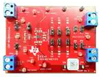
TPS22966EVM-007 Dual 6A Load Switch
The TPS22966EVM-007 evaluation module contains a dual channel, ultra low ON resistance, 6-A load
switch with controlled turn and adjustable rise time.
1
2
3
4
5
6
7
Contents
Description ................................................................................................................... 2
1.1
Typical Applications ................................................................................................ 2
1.2
Features ............................................................................................................. 2
Electrical Performance Specifications .................................................................................... 2
Schematic .................................................................................................................... 4
Layout ........................................................................................................................ 5
Test Setup ................................................................................................................... 7
5.1
Test Equipment ..................................................................................................... 7
5.2
Test Setup .......................................................................................................... 8
5.3
List of Test Points ................................................................................................ 10
5.4
Test Procedure ................................................................................................... 10
5.5
RON Test Procedure .............................................................................................. 11
5.6
tR, tON, tF, tOFF Test Procedure .................................................................................... 11
Performance Data and Typical Characteristic Curves ................................................................ 12
6.1
tR and tF Curves ................................................................................................... 12
6.2
6A Operation ...................................................................................................... 13
6.3
RON vs Input Voltage ............................................................................................. 14
6.4
RON vs Temperature .............................................................................................. 14
6.5
tR vs CT Capacitor Value ........................................................................................ 15
Bill of Materials ............................................................................................................. 15
List of Figures
1
TPS22966EVM-007 Schematic ........................................................................................... 4
2
TPS22966EVM-007 Top Assembly....................................................................................... 5
3
TPS22966EVM-007 Topside .............................................................................................. 6
4
TPS22966EVM-007 Bottomside .......................................................................................... 7
5
TPS22966EVM-007 Recommended Ron Test Set Up
6
TPS22966EVM-007 Recommended Trise Test Set Up
11
................................................................ 8
............................................................... 9
TPS22966EVM-007 tR and tF with VIN=5V, CT=1nF and Load =10Ω. ............................................. 12
TPS22966EVM-007 Turn-ON and Operation at 6A. .................................................................. 13
TPS22966EVM-007 RON .................................................................................................. 14
TPS22966EVM-007 RON vs Temperature .............................................................................. 14
TPS22966EVM-0077 tR vs CT cap ...................................................................................... 15
1
tR vs VIN vs CT capacitor .................................................................................................. 3
2
The Functions of Each Test Points
3
EVM Components List .................................................................................................... 15
7
8
9
10
List of Tables
SLVU757A – August 2012 – Revised March 2013
Submit Documentation Feedback
.....................................................................................
TPS22966EVM-007 Dual 6A Load Switch
Copyright © 2012–2013, Texas Instruments Incorporated
10
1
�Description
1
www.ti.com
Description
The TPS22966 device contains two N-channel MOSFETs that can operate over an input voltage range of
0.8V to 5.5 V and can support a maximum continuous current of up to 6-A per channel. Each switch is
independently controlled by an on/off input (ON1, ON2), which is capable of interfacing directly with lowvoltage GPIO control signals. In the TPS22966, a 260-Ω on-chip load resistor is added for quick output
discharge (QOD) when the switch is turned off. The rise time of the device is internally controlled in order
to avoid in-rush current and can be adjusted using a ceramic capacitor on the CTx pins. The TPS22966 is
available in a small, space-saving 2mm x 3mm 14-pin SON package with integrated thermal pad allowing
for high power dissipation.
The TPS22966 device is demonstrated using the TPS22966EVM-007 module. The TPS22966 Dual Load
Switch device can be configured in either a dual switch configuration or a parallel switch configuration
using the TPS22966EVM-007.
1.1
Typical Applications
●
●
●
●
1.2
● Set-top Boxes
● Industrial Systems
● Telecom Systems
Features
●
●
●
●
2
UltrabooksTM
Notebooks/Netbooks
Tablet PC
Consumer Electronics
Integrated dual channel load switch
Input voltage range: 0.8V to 5.5V
Ultra-low on-resistance (18 mΩ typical)
6A maximum continuous switch current
per channel
●
●
●
●
Low threshold control inputs
Adjustable slew-rate control
Quick Output Discharge transistor
SON 14-pin package with thermal pad
Electrical Performance Specifications
RON, CL = 0.1 µF at VIN
RON (mΩ)
(max)
Measured values at 25°C
VIN (V)
VIN1 - VOUT1
(V)
IOUT1 (A)
RON (mΩ)
VIN2 - VOUT2 (V)
IOUT2 (A)
RON (mΩ)
20.0
5
0.00378
0.208
17.93269231
0.00374
0.2077
18.00674049
20.0
3.3
0.003615
0.208
17.37980769
0.00363
0.2077
17.47713048
20.0
1.8
0.003634
0.208
17.47115385
0.00364
0.2077
17.52527684
20.0
1.5
0.00363
0.208
17.45192308
0.00363
0.2077
17.47713048
20.0
1.2
0.00362
0.208
17.40384615
0.00364
0.2077
17.52527684
20.0
0.8
0.00362
0.208
17.40384615
0.00364
0.2077
17.52527684
spacer
IIN(VIN-OFF) at 25°C
IIN(VIN-OFF)
(max)
2
VIN1, VIN2 (V)
VON1, VON2 = 0 V, VOUT1, VOUT2 = Open
IIN(VIN1-OFF) (µA)
IIN(VIN2-OFF) (µA)
1
5.0
0.098
0.075
1
3.3
0.031
0.017
1
1.8
0.012
0.007
1
0.8
0.001
0.007
TPS22966EVM-007 Dual 6A Load Switch
SLVU757A – August 2012 – Revised March 2013
Submit Documentation Feedback
Copyright © 2012–2013, Texas Instruments Incorporated
�Electrical Performance Specifications
www.ti.com
spacer
SWITCHING CHARACTERISTICS
VIN1 = 5.0V, VIN2 = 5.0 V, TA = 25C (unless otherwise noted)
Parameter
Each Channel
Test Condition
TYPICAL
tON
Turn on time
RL = 10 Ω, CL = 0.1 µF, CT = 270 pF
tOFF
Turn off time
RL = 10 Ω, CL = 0.1 µF, CT = 270 pF
20
tR
VOUT Rise time
RL = 10 Ω, CL = 0.1 µF, CT = 270 pF
580
tF
VOUT Fall time
RL = 10 Ω, CL = 0.1 µF, CT = 270 pF
20
tD
On delay time
RL = 10 Ω, CL = 0.1 µF, CT = 270 pF
50% tR
Unit
491
µs
Parametric Measurement Information
VIN1
VOUT1
CIN = 1 µF
ON
+
–
On1
CL
(A)
RL
CT1
OFF
TPS22966
GND
GND
GND
(Single channel show for clarity)
TEST CIRCUIT
Table 1. tR vs VIN vs CT capacitor
Rise Time (µs) 10%–90%, CL = 0.1 µF at VIN
Typical values at 25°C,25 V X7R 10% ceramic cap
CTx
Slew Rate
(µs/V)
(TYP)
5V
3.3V
1.8V
1.5V
1.2V
1.05V
1V
0.8V
0
38
188
130
52
44
38
35
33
29
220
101
505
336
182
152
121
106
101
81
270
116
580
384
209
174
139
122
116
93
470
175
877
580
316
263
210
184
175
140
680
238
1192
788
429
358
286
250
238
191
1000
339
1693
1107
609
508
406
256
339
271
2200
693
3464
2301
1247
1039
831
727
693
554
3300
1020
5098
3388
1835
1529
1224
1071
1020
816
4700
1440
7200
4769
2592
2160
1728
1512
1440
1152
10000
3004
15020
9991
5407
4506
3605
3154
3004
2403
spacer
SLVU757A – August 2012 – Revised March 2013
Submit Documentation Feedback
TPS22966EVM-007 Dual 6A Load Switch
Copyright © 2012–2013, Texas Instruments Incorporated
3
�4
TP1
1
2
TP2
TPS22966EVM-007 Dual 6A Load Switch
Copyright © 2012–2013, Texas Instruments Incorporated
1
ON2
TP11
JP2
C2
DNP
0V to 5.0V
C13
0.01uF
TP10
2.5V to 5.0V
C11
0.01uF
0V to 5.0V
C12
0.01uF
C4
1uF
TP4
VIN2
VIN2
ON2
VBIAS
ON1
VIN1
VIN1
U1
VIN2 SEN
TPS22966DPU
7
6
5
4
2
1
3
JP3
C3
1uF
TP9
C1
DNP
TP3
VIN1 SEN
ON1
VBIAS
JP1
DNP=Do Not Populate
0.8V to 5.5V
VIN2
J2
0.8V to 5.5V
VIN1
1
2
15
VOUT1
14
8
9
10
11
12
13
C6
1nF
C8
0.1uF
C5
0.1uF
VOUT2 SEN
TP6
VOUT2
VOUT2
CT2
GND
CT1
VOUT1
TP5
C9
1nF
C0603
VOUT1 SEN
JP4
C10
DNP
JP5
C7
DNP
TP13
JP6
JP7
TP14
R2
DNP
R1
DNP
JP8
JP9
1
J3
TP15
R4
DNP
R3
DNP
TP7
JP10
JP11
1
TP16
2
J4
TP12
VOUT1//VOUT2
6A Max.
JP12
JP13
6A Max.
VOUT2
TP8
VOUT1
2
3
PWPD
J1
Schematic
www.ti.com
Schematic
Figure 1. TPS22966EVM-007 Schematic
SLVU757A – August 2012 – Revised March 2013
Submit Documentation Feedback
�Layout
www.ti.com
Layout
TP13 TP13
J3
JP9
JP13
TP12
C10
C2
C10
R2
R4
JP12
J4
TP6
TP6
J4
JP8
R4
JP6
R2
JP4
JP10
JP12
C13
TP11
TP11
JP8
C8
JP6
C4
JP4
JP2
C2
C8
JP11
J3
TP12
C6
C4
C12
U1
C12
JP2
C9
1
C11
TP10
C13
JP13
JP9
JP11
JP7
JP7
C5
C11
TP10
C5
TP5
C6
C1
C7
JP1
C3
TP5
C9
JP3
R3
C3
U1
TPS22966EVM-007
JP5
JP1
JP3
R3
R1
R1
C1
C7
TP9
TP9
JP10
J1
TP1 TP1
J1
J2
TP2 TP2
TP8 TP8
J2
TP14 TP14
TP7 TP7
TP3 TP3
JP5
4
TP4
TP16
TP15
TP16
TP15
TP4
HVL007 Rev. A
Figure 2. TPS22966EVM-007 Top Assembly
SLVU757A – August 2012 – Revised March 2013
Submit Documentation Feedback
TPS22966EVM-007 Dual 6A Load Switch
Copyright © 2012–2013, Texas Instruments Incorporated
5
�Layout
www.ti.com
Figure 3. TPS22966EVM-007 Topside
6
TPS22966EVM-007 Dual 6A Load Switch
SLVU757A – August 2012 – Revised March 2013
Submit Documentation Feedback
Copyright © 2012–2013, Texas Instruments Incorporated
�Test Setup
www.ti.com
Figure 4. TPS22966EVM-007 Bottomside
5
Test Setup
5.1
Test Equipment
•
•
•
•
•
•
Voltage Source:
– 1 Power Source capable of 10V 15A
Multimeters:
– 2 voltmeters
Output Loads:
– Electronic Load or Resistor(If testing 6A operation of the switch at 5.5V a 33W power rated resistor
is needed)
Oscilloscope:
– 4 channel 100MHz
Signal Generator:
– Dual Channel Preferred
Recommended Wire Gauge: 18 AWG
SLVU757A – August 2012 – Revised March 2013
Submit Documentation Feedback
TPS22966EVM-007 Dual 6A Load Switch
Copyright © 2012–2013, Texas Instruments Incorporated
7
�Test Setup
Test Setup
TP13 TP13
J3
JP13
JP10
JP12
JP12
JP9
J3
TP12
JP4
JP6
JP8
R2
R4
C2
JP8
C8
JP6
C4
TP11
TP11
C10
C8
C10
R2
R4
J4
TP6
TP6
J4
JP1
C13
JP13
TP12
C6
C4
C12
U1
JP11
C6
JP3
C3
C9
TP5
JP11
JP9
JP7
C7
JP7
JP4
JP2
C2
C5
C13
C12
JP2
C5
U1
TP10
C11
TP10
C3
TP5
C9
C11
1
TPS22966EVM-007
JP5
JP1
JP3
R3
R1
R3
C1
C7
TP9
TP9
R1
C1
JP10
J1
TP1 TP1
J1
J2
TP2 TP2
TP16
TP8 TP8
J2
TP14 TP14
TP7 TP7
TP3 TP3
JP5
5.2
www.ti.com
TP4
TP4
TP16
TP15
TP15
HVL007 Rev. A
Figure 5. TPS22966EVM-007 Recommended Ron Test Set Up
8
TPS22966EVM-007 Dual 6A Load Switch
SLVU757A – August 2012 – Revised March 2013
Submit Documentation Feedback
Copyright © 2012–2013, Texas Instruments Incorporated
�Test Setup
www.ti.com
TP1
TP3 TP3
TP13 TP13
JP11
JP10
JP12
J3
JP9
JP13
J3
TP12
TP12
JP8
C10
C2
C10
R2
R4
J4
TP6
TP6
J4
JP6
R4
JP4
R2
C4
TP11
TP11
JP8
C8
JP6
C8
C4
JP13
JP7
JP1
C13
U1
JP11
JP10
JP9
JP5
C7
JP7
TP5
C6
C12
C9
JP4
JP2
JP2
C5
C6
C12
C2
C5
C13
U1
C11
TP10
C3
C3
C11
TP5
C9
C1
R3
JP3
TP10
R3
R1
JP5
JP1
1
TPS22966EVM-007
JP3
C7
TP9
TP9
R1
C1
JP12
J1
J1
J2
TP2 TP2
TP16
TP8 TP8
J2
TP14 TP14
TP7 TP7
TP1
TP4
TP4
TP16
TP15
TP15
HVL007 Rev. A
Figure 6. TPS22966EVM-007 Recommended Trise Test Set Up
SLVU757A – August 2012 – Revised March 2013
Submit Documentation Feedback
TPS22966EVM-007 Dual 6A Load Switch
Copyright © 2012–2013, Texas Instruments Incorporated
9
�Test Setup
5.3
www.ti.com
List of Test Points
Table 2. The Functions of Each Test Points
5.4
Test Points
Name
Description
J1
VIN1
DC Input to VIN1
J2
VIN2
DC Input for VIN2
JP1
VBIAS
Connects VBIAS to VIN1
JP2
C2
Connects C2 to VIN2
JP3
C1
Connects C1 to VIN1
JP4
C10
Connects C10 to VOUT2
JP5
C7
Connects C7 to VOUT1
JP6
R2
Connects R2 to VOUT2
JP7
R1
Connects R1 to VOUT1
JP8
R4
Connects R4 to VOUT2
JP9
R3
Connects R3 to VOUT1
JP10, JP11,
JP12, JP13
VOUT1 // VOUT2
Shorts VOUT1 and VOUT2 to VOUT1//VOUT2 used in parallel switch configuration
TP1
VIN1
VIN1 of TPS22966
TP2
VIN2
VIN2 of TPS22966
TP3
VIN1 SEN
Sense connect to VIN1 of TPS22966
TP4
VIN2 SEN
Sense connect to VIN2 of TPS22966
TP5
VOUT1
VOUT1 of TPS22966
TP6
VOUT2
VOUT2 of TPS22966
TP7
VOUT1 SEN
Sense connect to VOUT1 of TPS22966
TP8
VOUT2 SEN
Sense connect to VOUT2 of TPS22966
TP9
ON1
ON1 of TPS22966
TP10
VBIAS
VBIAS of TPS22966
TP11
ON2
ON2 of TPS22966
TP12
VOUT1 // VOUT2
VOUT1 VOUT2 connected in parallel configuration
TP13
AGND
Ground Connection
TP14
AGND
Ground Connection
TP15
AGND
Ground Connection
TP16
AGND
Ground Connection
Test Procedure
Figure 5 shows a typical setup for the RON test of the EVM. VBIAS voltage must be present for the device
to function, keep this voltage level constant between 2.5V-5.25V. Adding a shunt across JP1 will connect
the VBIAS pin to VIN1. When testing with VIN1 below 2.5V JP1 shunt must be removed and VBIAS tied to
another voltage source. It is recommended to keep VBIAS voltage level at 5V. Datasheet specifications
were taken with VBIAS = 5V.
10
TPS22966EVM-007 Dual 6A Load Switch
SLVU757A – August 2012 – Revised March 2013
Submit Documentation Feedback
Copyright © 2012–2013, Texas Instruments Incorporated
�Test Setup
www.ti.com
5.5
RON Test Procedure
1.
2.
3.
4.
Setup the EVM per Figure 5.
Set SOURCE1 level to 5.0V.
Place a shunt across JP1.
Connect ON1 to a DC source between 1.05v and 5.5v, SOURCE1 supply can be used for this. (When
testing RON it is desired to have the switch operating in the always ON condition.)
5. Connect ON2 to GND. This keeps switch 2 in the off state.
6. Place a load on VOUT1 and VOUT2.
7. Turn on SOURCE1.
8. Record the voltage reading from METER1, record the input current reading from SOURCE1. Calculate
Ron by dividing METER1 voltage level by the current reading from SOURCE1. The result will be the
RON value for switch 1.
9. Turn SOURCE1 off.
10. Remove ON1 from SOURCE1 and connect to GND.
11. Remove ON2 from GND and connect to SOURCE1.
12. Turn SOURCE1 on.
13. Record the voltage reading from METER2, record the input current reading from SOURCE1. Calculate
RON by dividing the voltage reading of METER2 by the current reading from SOURCE1. The results will
be the RON value for switch 2.
14. Turn SOURCE1 off.
5.6
tR, tON, tF, tOFF Test Procedure
1. The rise time (tR) is selected by the CT capacitor value on each switch channel. Table 1 shows CT
value and the associated tR value. The EVM is shipped with a default CT value of 1nF.
2. Set up the EVM per Figure 6
3. Set SOURCE1 level to 5.0V.
4. Place a shunt across JP1.
5. Place a load on VOUT1 and VOUT2 (a 10Ω, 3.25W resistor is recommended for this test).
6. Set Signal Generator output to 0-2Vpp, 10-100Hz, and 25% duty cycle.
7. Turn SOURCE1 on.
8. Enable the Signal Generator output.
9. Rise time (tR) and turn-on time (tON) can be observed from the Oscilloscope channel 1 for switch 1 and
channel 4 for switch 2. A detailed description of tR, tON, tF and tOFF are listed in the TPS22966 Datasheet
under the Switching Characteristics Section.
10. Turn SOURCE1 off and disable the signal Generator output.
SLVU757A – August 2012 – Revised March 2013
Submit Documentation Feedback
TPS22966EVM-007 Dual 6A Load Switch
Copyright © 2012–2013, Texas Instruments Incorporated
11
�Performance Data and Typical Characteristic Curves
6
www.ti.com
Performance Data and Typical Characteristic Curves
Figure 7 through Figure 11 present typical performance curves for TPS22966EVM-007.
6.1
tR and tF Curves
Figure 7. TPS22966EVM-007 tR and tF with VIN=5V, CT=1nF and Load =10Ω.
12
TPS22966EVM-007 Dual 6A Load Switch
SLVU757A – August 2012 – Revised March 2013
Submit Documentation Feedback
Copyright © 2012–2013, Texas Instruments Incorporated
�Performance Data and Typical Characteristic Curves
www.ti.com
6.2
6A Operation
Figure 8. TPS22966EVM-007 Turn-ON and Operation at 6A.
SLVU757A – August 2012 – Revised March 2013
Submit Documentation Feedback
TPS22966EVM-007 Dual 6A Load Switch
Copyright © 2012–2013, Texas Instruments Incorporated
13
�Performance Data and Typical Characteristic Curves
6.3
www.ti.com
RON vs Input Voltage
19
18.8
18.6
Ron (mΩ)
18.4
u1sw1
u1sw2
u5sw1
u5sw2
u3sw1
u3sw2
Iload = 200 mA
18.2
18
17.8
17.6
17.4
17.2
17
0.8
1.3
1.8
2.3
2.8
3.3
Input Voltage (V)
3.8
4.3
4.8
G001
Figure 9. TPS22966EVM-007 RON
6.4
RON vs Temperature
24
Iload = 200mA
22
Ron (mΩ)
20
18
16
u1sw1
u3sw1
u5sw1
u1sw2
u3sw2
u5sw2
14
12
10
−40
−20
0
20
40
Temperature (°C)
60
80
100
G002
Figure 10. TPS22966EVM-007 RON vs Temperature
14
TPS22966EVM-007 Dual 6A Load Switch
SLVU757A – August 2012 – Revised March 2013
Submit Documentation Feedback
Copyright © 2012–2013, Texas Instruments Incorporated
�Bill of Materials
www.ti.com
6.5
tR vs CT Capacitor Value
18000
Vin5.0v
Vin3.3v
Vin1.8v
Vin1.5v
Vin1.2v
Vin1.0v
Vin0.8v
16000
14000
Trise (µs)
12000
Iload = 0 mA
10000
8000
6000
4000
2000
0
0
2000
4000
6000
8000
10000
CT (pF)
G003
Figure 11. TPS22966EVM-0077 tR vs CT cap
7
Bill of Materials
Table 3 is the EVM componets list according to the schematic shown in Figure 1.
Table 3. EVM Components List
Count
RefDes
Value
Description
Size
Part Number
MFR
0
C1, C2, C7, C10
DNP
Capacitor, Ceramic, 25V, X7R, 20%
603
Std
Std
3
C11, C12, C13
0.01µF
Capacitor, Ceramic, 16V, X7R, 20%
603
Std
Std
2
C3, C4
1µF
Capacitor, Ceramic,16V, X7R, 20%
603
Std
Std
2
C5, C8
0.1µF
Capacitor, Ceramic, 25V, X7R, 20%
603
Std
Std
2
C6, C9
1nF
Capacitor, Ceramic, 25V, X7R, 20%
603
Std
Std
1
JP1
PEC02SAAN
Header, Male 2-pin, 100mil spacing
0.100 inch x 2
PEC02SAAN
Sullins
12
JP2, JP3, JP4,
JP5, JP6, JP7,
JP8, JP9, JP10,
JP11, JP12,
JP13
PEC02SAAN
Header, Male 2-pin, 100mil spacing
0.100 inch x 2
PEC02SAAN
Sullins
0
R1, R2, R3, R4
DNP
Resistor, Chip, 1/16W, x%
805
Std
Std
12
TP1, TP2, TP3,
TP4, TP5, TP6,
TP7, TP8, TP9,
TP10, TP11,
TP12
5010
Test Point, Red, Thru Hole Compact Style
0.125 x 0.125 inch
5010
Keystone
4
TP13, TP14,
TP15, TP16
5011
Test Point, Black, Thru Hole Compact Style
0.125 x 0.125 inch
5011
Keystone
4
J1, J2, J3, J4
ED120/2DS
Terminal Block, 2-pin, 15-A, 5.1mm
0.512 inch
ED120/2DS
OST
1
U1
TPS22966DPU
IC, 6-A Dual Load Switch With Controlled Turn-On
PWSON
TPS22966DPU
TI
1
--
HVL007
Any
929950-00
3M
1
PCB, 2.98 In x 2.22 In x 0.062 In
Shunt, Black
100-mil
Notes: 1. These assemblies are ESD sensitive, ESD precautions shall be observed.
2. These assemblies must be clean and free from flux and all contaminants. Use of no clean flux is not acceptable.
3. These assemblies must comply with workmanship standards IPC-A-610 Class 2.
4. Ref designators marked with an asterisk ('**') cannot be substituted. All other components can be substituted with equivalent MFG's components.
SLVU757A – August 2012 – Revised March 2013
Submit Documentation Feedback
TPS22966EVM-007 Dual 6A Load Switch
Copyright © 2012–2013, Texas Instruments Incorporated
15
�Revision History
www.ti.com
Revision History
Changes from Original (August 2012) to A Revision ..................................................................................................... Page
•
Changed DCN to DPU for Value and Part Number in line item 12 of BOM ..................................................... 15
NOTE: Page numbers for previous revisions may differ from page numbers in the current version.
16
Revision History
SLVU757A – August 2012 – Revised March 2013
Submit Documentation Feedback
Copyright © 2012–2013, Texas Instruments Incorporated
�EVALUATION BOARD/KIT/MODULE (EVM) ADDITIONAL TERMS
Texas Instruments (TI) provides the enclosed Evaluation Board/Kit/Module (EVM) under the following conditions:
The user assumes all responsibility and liability for proper and safe handling of the goods. Further, the user indemnifies TI from all claims
arising from the handling or use of the goods.
Should this evaluation board/kit not meet the specifications indicated in the User’s Guide, the board/kit may be returned within 30 days from
the date of delivery for a full refund. THE FOREGOING LIMITED WARRANTY IS THE EXCLUSIVE WARRANTY MADE BY SELLER TO
BUYER AND IS IN LIEU OF ALL OTHER WARRANTIES, EXPRESSED, IMPLIED, OR STATUTORY, INCLUDING ANY WARRANTY OF
MERCHANTABILITY OR FITNESS FOR ANY PARTICULAR PURPOSE. EXCEPT TO THE EXTENT OF THE INDEMNITY SET FORTH
ABOVE, NEITHER PARTY SHALL BE LIABLE TO THE OTHER FOR ANY INDIRECT, SPECIAL, INCIDENTAL, OR CONSEQUENTIAL
DAMAGES.
Please read the User's Guide and, specifically, the Warnings and Restrictions notice in the User's Guide prior to handling the product. This
notice contains important safety information about temperatures and voltages. For additional information on TI's environmental and/or safety
programs, please visit www.ti.com/esh or contact TI.
No license is granted under any patent right or other intellectual property right of TI covering or relating to any machine, process, or
combination in which such TI products or services might be or are used. TI currently deals with a variety of customers for products, and
therefore our arrangement with the user is not exclusive. TI assumes no liability for applications assistance, customer product design,
software performance, or infringement of patents or services described herein.
REGULATORY COMPLIANCE INFORMATION
As noted in the EVM User’s Guide and/or EVM itself, this EVM and/or accompanying hardware may or may not be subject to the Federal
Communications Commission (FCC) and Industry Canada (IC) rules.
For EVMs not subject to the above rules, this evaluation board/kit/module is intended for use for ENGINEERING DEVELOPMENT,
DEMONSTRATION OR EVALUATION PURPOSES ONLY and is not considered by TI to be a finished end product fit for general consumer
use. It generates, uses, and can radiate radio frequency energy and has not been tested for compliance with the limits of computing
devices pursuant to part 15 of FCC or ICES-003 rules, which are designed to provide reasonable protection against radio frequency
interference. Operation of the equipment may cause interference with radio communications, in which case the user at his own expense will
be required to take whatever measures may be required to correct this interference.
General Statement for EVMs including a radio
User Power/Frequency Use Obligations: This radio is intended for development/professional use only in legally allocated frequency and
power limits. Any use of radio frequencies and/or power availability of this EVM and its development application(s) must comply with local
laws governing radio spectrum allocation and power limits for this evaluation module. It is the user’s sole responsibility to only operate this
radio in legally acceptable frequency space and within legally mandated power limitations. Any exceptions to this are strictly prohibited and
unauthorized by Texas Instruments unless user has obtained appropriate experimental/development licenses from local regulatory
authorities, which is responsibility of user including its acceptable authorization.
For EVMs annotated as FCC – FEDERAL COMMUNICATIONS COMMISSION Part 15 Compliant
Caution
This device complies with part 15 of the FCC Rules. Operation is subject to the following two conditions: (1) This device may not cause
harmful interference, and (2) this device must accept any interference received, including interference that may cause undesired operation.
Changes or modifications not expressly approved by the party responsible for compliance could void the user's authority to operate the
equipment.
FCC Interference Statement for Class A EVM devices
This equipment has been tested and found to comply with the limits for a Class A digital device, pursuant to part 15 of the FCC Rules.
These limits are designed to provide reasonable protection against harmful interference when the equipment is operated in a commercial
environment. This equipment generates, uses, and can radiate radio frequency energy and, if not installed and used in accordance with the
instruction manual, may cause harmful interference to radio communications. Operation of this equipment in a residential area is likely to
cause harmful interference in which case the user will be required to correct the interference at his own expense.
�FCC Interference Statement for Class B EVM devices
This equipment has been tested and found to comply with the limits for a Class B digital device, pursuant to part 15 of the FCC Rules.
These limits are designed to provide reasonable protection against harmful interference in a residential installation. This equipment
generates, uses and can radiate radio frequency energy and, if not installed and used in accordance with the instructions, may cause
harmful interference to radio communications. However, there is no guarantee that interference will not occur in a particular installation. If
this equipment does cause harmful interference to radio or television reception, which can be determined by turning the equipment off and
on, the user is encouraged to try to correct the interference by one or more of the following measures:
• Reorient or relocate the receiving antenna.
• Increase the separation between the equipment and receiver.
• Connect the equipment into an outlet on a circuit different from that to which the receiver is connected.
• Consult the dealer or an experienced radio/TV technician for help.
For EVMs annotated as IC – INDUSTRY CANADA Compliant
This Class A or B digital apparatus complies with Canadian ICES-003.
Changes or modifications not expressly approved by the party responsible for compliance could void the user’s authority to operate the
equipment.
Concerning EVMs including radio transmitters
This device complies with Industry Canada licence-exempt RSS standard(s). Operation is subject to the following two conditions: (1) this
device may not cause interference, and (2) this device must accept any interference, including interference that may cause undesired
operation of the device.
Concerning EVMs including detachable antennas
Under Industry Canada regulations, this radio transmitter may only operate using an antenna of a type and maximum (or lesser) gain
approved for the transmitter by Industry Canada. To reduce potential radio interference to other users, the antenna type and its gain should
be so chosen that the equivalent isotropically radiated power (e.i.r.p.) is not more than that necessary for successful communication.
This radio transmitter has been approved by Industry Canada to operate with the antenna types listed in the user guide with the maximum
permissible gain and required antenna impedance for each antenna type indicated. Antenna types not included in this list, having a gain
greater than the maximum gain indicated for that type, are strictly prohibited for use with this device.
Cet appareil numérique de la classe A ou B est conforme à la norme NMB-003 du Canada.
Les changements ou les modifications pas expressément approuvés par la partie responsable de la conformité ont pu vider l’autorité de
l'utilisateur pour actionner l'équipement.
Concernant les EVMs avec appareils radio
Le présent appareil est conforme aux CNR d'Industrie Canada applicables aux appareils radio exempts de licence. L'exploitation est
autorisée aux deux conditions suivantes : (1) l'appareil ne doit pas produire de brouillage, et (2) l'utilisateur de l'appareil doit accepter tout
brouillage radioélectrique subi, même si le brouillage est susceptible d'en compromettre le fonctionnement.
Concernant les EVMs avec antennes détachables
Conformément à la réglementation d'Industrie Canada, le présent émetteur radio peut fonctionner avec une antenne d'un type et d'un gain
maximal (ou inférieur) approuvé pour l'émetteur par Industrie Canada. Dans le but de réduire les risques de brouillage radioélectrique à
l'intention des autres utilisateurs, il faut choisir le type d'antenne et son gain de sorte que la puissance isotrope rayonnée équivalente
(p.i.r.e.) ne dépasse pas l'intensité nécessaire à l'établissement d'une communication satisfaisante.
Le présent émetteur radio a été approuvé par Industrie Canada pour fonctionner avec les types d'antenne énumérés dans le manuel
d’usage et ayant un gain admissible maximal et l'impédance requise pour chaque type d'antenne. Les types d'antenne non inclus dans
cette liste, ou dont le gain est supérieur au gain maximal indiqué, sont strictement interdits pour l'exploitation de l'émetteur.
SPACER
SPACER
SPACER
SPACER
SPACER
SPACER
SPACER
SPACER
�【Important Notice for Users of this Product in Japan】
】
This development kit is NOT certified as Confirming to Technical Regulations of Radio Law of Japan
If you use this product in Japan, you are required by Radio Law of Japan to follow the instructions below with respect to this product:
1.
2.
3.
Use this product in a shielded room or any other test facility as defined in the notification #173 issued by Ministry of Internal Affairs and
Communications on March 28, 2006, based on Sub-section 1.1 of Article 6 of the Ministry’s Rule for Enforcement of Radio Law of
Japan,
Use this product only after you obtained the license of Test Radio Station as provided in Radio Law of Japan with respect to this
product, or
Use of this product only after you obtained the Technical Regulations Conformity Certification as provided in Radio Law of Japan with
respect to this product. Also, please do not transfer this product, unless you give the same notice above to the transferee. Please note
that if you could not follow the instructions above, you will be subject to penalties of Radio Law of Japan.
Texas Instruments Japan Limited
(address) 24-1, Nishi-Shinjuku 6 chome, Shinjuku-ku, Tokyo, Japan
http://www.tij.co.jp
【ご使用にあたっての注】
本開発キットは技術基準適合証明を受けておりません。
本製品のご使用に際しては、電波法遵守のため、以下のいずれかの措置を取っていただく必要がありますのでご注意ください。
1.
2.
3.
電波法施行規則第6条第1項第1号に基づく平成18年3月28日総務省告示第173号で定められた電波暗室等の試験設備でご使用いただく。
実験局の免許を取得後ご使用いただく。
技術基準適合証明を取得後ご使用いただく。
なお、本製品は、上記の「ご使用にあたっての注意」を譲渡先、移転先に通知しない限り、譲渡、移転できないものとします。
上記を遵守頂けない場合は、電波法の罰則が適用される可能性があることをご留意ください。
日本テキサス・インスツルメンツ株式会社
東京都新宿区西新宿6丁目24番1号
西新宿三井ビル
http://www.tij.co.jp
SPACER
SPACER
SPACER
SPACER
SPACER
SPACER
SPACER
SPACER
SPACER
SPACER
SPACER
SPACER
SPACER
SPACER
SPACER
SPACER
SPACER
�EVALUATION BOARD/KIT/MODULE (EVM)
WARNINGS, RESTRICTIONS AND DISCLAIMERS
For Feasibility Evaluation Only, in Laboratory/Development Environments. Unless otherwise indicated, this EVM is not a finished
electrical equipment and not intended for consumer use. It is intended solely for use for preliminary feasibility evaluation in
laboratory/development environments by technically qualified electronics experts who are familiar with the dangers and application risks
associated with handling electrical mechanical components, systems and subsystems. It should not be used as all or part of a finished end
product.
Your Sole Responsibility and Risk. You acknowledge, represent and agree that:
1.
2.
3.
4.
You have unique knowledge concerning Federal, State and local regulatory requirements (including but not limited to Food and Drug
Administration regulations, if applicable) which relate to your products and which relate to your use (and/or that of your employees,
affiliates, contractors or designees) of the EVM for evaluation, testing and other purposes.
You have full and exclusive responsibility to assure the safety and compliance of your products with all such laws and other applicable
regulatory requirements, and also to assure the safety of any activities to be conducted by you and/or your employees, affiliates,
contractors or designees, using the EVM. Further, you are responsible to assure that any interfaces (electronic and/or mechanical)
between the EVM and any human body are designed with suitable isolation and means to safely limit accessible leakage currents to
minimize the risk of electrical shock hazard.
You will employ reasonable safeguards to ensure that your use of the EVM will not result in any property damage, injury or death, even
if the EVM should fail to perform as described or expected.
You will take care of proper disposal and recycling of the EVM’s electronic components and packing materials.
Certain Instructions. It is important to operate this EVM within TI’s recommended specifications and environmental considerations per the
user guidelines. Exceeding the specified EVM ratings (including but not limited to input and output voltage, current, power, and
environmental ranges) may cause property damage, personal injury or death. If there are questions concerning these ratings please contact
a TI field representative prior to connecting interface electronics including input power and intended loads. Any loads applied outside of the
specified output range may result in unintended and/or inaccurate operation and/or possible permanent damage to the EVM and/or
interface electronics. Please consult the EVM User's Guide prior to connecting any load to the EVM output. If there is uncertainty as to the
load specification, please contact a TI field representative. During normal operation, some circuit components may have case temperatures
greater than 60°C as long as the input and output are maintained at a normal ambient operating temperature. These components include
but are not limited to linear regulators, switching transistors, pass transistors, and current sense resistors which can be identified using the
EVM schematic located in the EVM User's Guide. When placing measurement probes near these devices during normal operation, please
be aware that these devices may be very warm to the touch. As with all electronic evaluation tools, only qualified personnel knowledgeable
in electronic measurement and diagnostics normally found in development environments should use these EVMs.
Agreement to Defend, Indemnify and Hold Harmless. You agree to defend, indemnify and hold TI, its licensors and their representatives
harmless from and against any and all claims, damages, losses, expenses, costs and liabilities (collectively, "Claims") arising out of or in
connection with any use of the EVM that is not in accordance with the terms of the agreement. This obligation shall apply whether Claims
arise under law of tort or contract or any other legal theory, and even if the EVM fails to perform as described or expected.
Safety-Critical or Life-Critical Applications. If you intend to evaluate the components for possible use in safety critical applications (such
as life support) where a failure of the TI product would reasonably be expected to cause severe personal injury or death, such as devices
which are classified as FDA Class III or similar classification, then you must specifically notify TI of such intent and enter into a separate
Assurance and Indemnity Agreement.
Mailing Address: Texas Instruments, Post Office Box 655303, Dallas, Texas 75265
Copyright © 2013, Texas Instruments Incorporated
�IMPORTANT NOTICE
Texas Instruments Incorporated and its subsidiaries (TI) reserve the right to make corrections, enhancements, improvements and other
changes to its semiconductor products and services per JESD46, latest issue, and to discontinue any product or service per JESD48, latest
issue. Buyers should obtain the latest relevant information before placing orders and should verify that such information is current and
complete. All semiconductor products (also referred to herein as “components”) are sold subject to TI’s terms and conditions of sale
supplied at the time of order acknowledgment.
TI warrants performance of its components to the specifications applicable at the time of sale, in accordance with the warranty in TI’s terms
and conditions of sale of semiconductor products. Testing and other quality control techniques are used to the extent TI deems necessary
to support this warranty. Except where mandated by applicable law, testing of all parameters of each component is not necessarily
performed.
TI assumes no liability for applications assistance or the design of Buyers’ products. Buyers are responsible for their products and
applications using TI components. To minimize the risks associated with Buyers’ products and applications, Buyers should provide
adequate design and operating safeguards.
TI does not warrant or represent that any license, either express or implied, is granted under any patent right, copyright, mask work right, or
other intellectual property right relating to any combination, machine, or process in which TI components or services are used. Information
published by TI regarding third-party products or services does not constitute a license to use such products or services or a warranty or
endorsement thereof. Use of such information may require a license from a third party under the patents or other intellectual property of the
third party, or a license from TI under the patents or other intellectual property of TI.
Reproduction of significant portions of TI information in TI data books or data sheets is permissible only if reproduction is without alteration
and is accompanied by all associated warranties, conditions, limitations, and notices. TI is not responsible or liable for such altered
documentation. Information of third parties may be subject to additional restrictions.
Resale of TI components or services with statements different from or beyond the parameters stated by TI for that component or service
voids all express and any implied warranties for the associated TI component or service and is an unfair and deceptive business practice.
TI is not responsible or liable for any such statements.
Buyer acknowledges and agrees that it is solely responsible for compliance with all legal, regulatory and safety-related requirements
concerning its products, and any use of TI components in its applications, notwithstanding any applications-related information or support
that may be provided by TI. Buyer represents and agrees that it has all the necessary expertise to create and implement safeguards which
anticipate dangerous consequences of failures, monitor failures and their consequences, lessen the likelihood of failures that might cause
harm and take appropriate remedial actions. Buyer will fully indemnify TI and its representatives against any damages arising out of the use
of any TI components in safety-critical applications.
In some cases, TI components may be promoted specifically to facilitate safety-related applications. With such components, TI’s goal is to
help enable customers to design and create their own end-product solutions that meet applicable functional safety standards and
requirements. Nonetheless, such components are subject to these terms.
No TI components are authorized for use in FDA Class III (or similar life-critical medical equipment) unless authorized officers of the parties
have executed a special agreement specifically governing such use.
Only those TI components which TI has specifically designated as military grade or “enhanced plastic” are designed and intended for use in
military/aerospace applications or environments. Buyer acknowledges and agrees that any military or aerospace use of TI components
which have not been so designated is solely at the Buyer's risk, and that Buyer is solely responsible for compliance with all legal and
regulatory requirements in connection with such use.
TI has specifically designated certain components as meeting ISO/TS16949 requirements, mainly for automotive use. In any case of use of
non-designated products, TI will not be responsible for any failure to meet ISO/TS16949.
Products
Applications
Audio
www.ti.com/audio
Automotive and Transportation
www.ti.com/automotive
Amplifiers
amplifier.ti.com
Communications and Telecom
www.ti.com/communications
Data Converters
dataconverter.ti.com
Computers and Peripherals
www.ti.com/computers
DLP® Products
www.dlp.com
Consumer Electronics
www.ti.com/consumer-apps
DSP
dsp.ti.com
Energy and Lighting
www.ti.com/energy
Clocks and Timers
www.ti.com/clocks
Industrial
www.ti.com/industrial
Interface
interface.ti.com
Medical
www.ti.com/medical
Logic
logic.ti.com
Security
www.ti.com/security
Power Mgmt
power.ti.com
Space, Avionics and Defense
www.ti.com/space-avionics-defense
Microcontrollers
microcontroller.ti.com
Video and Imaging
www.ti.com/video
RFID
www.ti-rfid.com
OMAP Applications Processors
www.ti.com/omap
TI E2E Community
e2e.ti.com
Wireless Connectivity
www.ti.com/wirelessconnectivity
Mailing Address: Texas Instruments, Post Office Box 655303, Dallas, Texas 75265
Copyright © 2013, Texas Instruments Incorporated
�