Order
Now
Product
Folder
Support &
Community
Tools &
Software
Technical
Documents
TPS22968, TPS22968N
SLVSCG3F – JANUARY 2014 – REVISED JULY 2017
TPS22968 Dual Channel, Ultra-Low Resistance Load Switch
1 Features
2 Applications
•
•
•
•
•
•
•
•
•
1
•
•
•
•
•
•
•
•
•
•
•
Integrated Dual Channel Load Switch
Input Voltage Range: 0.8 V to 5.5 V
VBIAS Voltage Range: 2.5 V to 5.5 V
– Ideal for 1S Battery Configuration
Ultra-Low RON Resistance
– RON = 27 mΩ at VIN = 5 V (VBIAS = 5 V)
– RON = 25 mΩ at VIN = 3.3 V (VBIAS = 5 V)
– RON = 25 mΩ at VIN = 1.8 V (VBIAS = 5 V)
4-A Maximum Continuous Switch Current per
Channel
Low Quiescent Current
– 55 µA at VBIAS = 5 V (Both Channels)
– 55 µA at VBIAS = 5 V (Single Channel)
Low Control Input Threshold Enables Use of
1.2-,1.8-, 2.5-, 3.3-V Logic
Configurable Rise Time(1)
Quick Output Discharge (QOD)(2) (Optional)
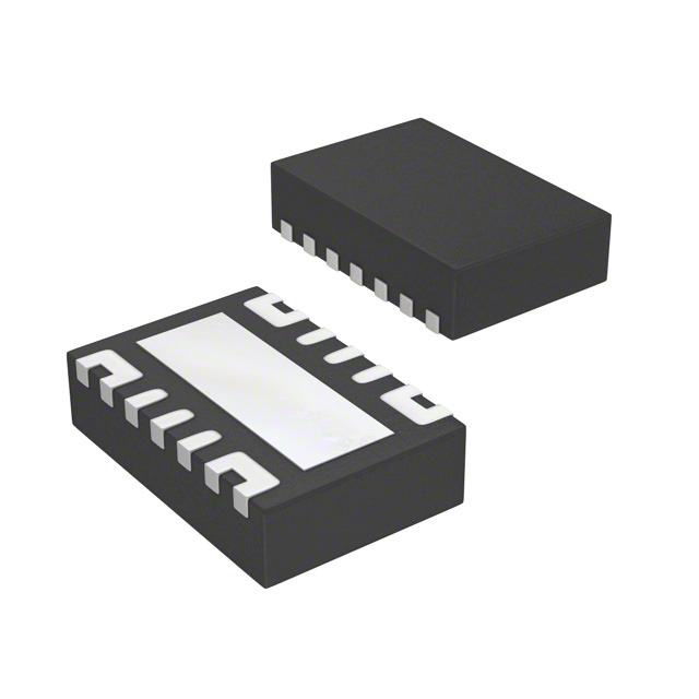
SON 14-Pin Package with Thermal Pad
ESD Performance Tested per JEDEC Standard
– 2-kV HBM and 1-kV CDM
Latch-Up Performance Exceeds 100 mA per
JESD 78, Class II
GPIO Enable – Active High
TPS22968N: Product Preview Only
Ultrabook™
Notebooks and Netbooks
Tablets
Consumer Electronics
Set-Top Boxes
Telecom Systems
3 Description
The TPS22968x is a small, ultra-low RON, dualchannel load switch with controlled turn on. The
device contains two N-channel MOSFETs that can
operate over an input voltage range of 0.8 to 5.5 V
and can support a maximum continuous current of
4 A per channel. Each switch is independently
controlled by an on and off input (ON1 and ON2),
which is capable of interfacing directly with lowvoltage control signals. In TPS22968, a 270-Ω onchip load resistor is added for output quick discharge
when switch is turned off.
The TPS22968x is available in a small, space-saving
package (DPU) with integrated thermal pad allowing
for high power dissipation. The device is
characterized for operation over the free-air
temperature range of –40 to +105°C.
Device Information (1)
PART NUMBER
(1)
See the Application Information section for CT value vs. rise
time
(2)
This feature discharges the output of the switch to GND
through a 270-Ω resistor, preventing the output from floating.
PACKAGE
TPS22968
TPS22968N
WSON (14)
BODY SIZE (NOM)
3.00 mm × 2.00 mm
(1) For all available packages, see the orderable addendum at
the end of the data sheet.
Typical Application Schematic
Dual Power
Supply
ON
CIN
OFF
VIN1
VOUT1
ON1
CT1
CL
RL
CT2
VBIAS
Or
GND
Dual DC/DC
converter
VOUT2
CIN
ON
ON2
CL
OFF
TPS22968x
RL
GND
GND
Copyright © 2016, Texas Instruments Incorporated
1
An IMPORTANT NOTICE at the end of this data sheet addresses availability, warranty, changes, use in safety-critical applications,
intellectual property matters and other important disclaimers. PRODUCTION DATA.
�TPS22968, TPS22968N
SLVSCG3F – JANUARY 2014 – REVISED JULY 2017
www.ti.com
Table of Contents
1
2
3
4
5
6
7
Features ..................................................................
Applications ...........................................................
Description .............................................................
Revision History.....................................................
Device Comparison ...............................................
Pin Configuration and Functions .........................
Specifications.........................................................
7.1
7.2
7.3
7.4
7.5
7.6
7.7
7.8
7.9
8
9
1
1
1
2
4
4
5
Absolute Maximum Ratings ...................................... 5
ESD Ratings.............................................................. 5
Recommended Operating Conditions....................... 5
Thermal Information .................................................. 5
Electrical Characteristics (VBIAS = 5 V) ..................... 6
Electrical Characteristics (VBIAS = 2.5 V) .................. 7
Switching Characteristics .......................................... 8
Typical DC Characteristics........................................ 8
Typical AC Characteristics...................................... 12
Parameter Measurement Information ................ 14
Detailed Description ............................................ 15
9.1 Overview ................................................................. 15
9.2 Functional Block Diagram ....................................... 15
9.3 Feature Description................................................. 16
9.4 Device Functional Modes........................................ 17
10 Application and Implementation........................ 18
10.1 Application Information.......................................... 18
10.2 Typical Application ................................................ 21
11 Power Supply Recommendations ..................... 24
12 Layout................................................................... 24
12.1 Layout Guidelines ................................................. 24
12.2 Layout Example .................................................... 24
13 Device and Documentation Support ................. 25
13.1
13.2
13.3
13.4
13.5
13.6
13.7
13.8
Device Support ....................................................
Documentation Support .......................................
Related Links ........................................................
Receiving Notification of Documentation Updates
Community Resources..........................................
Trademarks ...........................................................
Electrostatic Discharge Caution ............................
Glossary ................................................................
25
25
25
25
25
25
26
26
14 Mechanical, Packaging, and Orderable
Information ........................................................... 26
4 Revision History
Changes from Revision D (March 2016) to Revision E
•
Page
Changed QOD description from (TPS22968 only) to (Optional) in Features section ............................................................ 1
Changes from Revision E (July 2016) to Revision F
•
Page
Changed Functional Block Diagram ....................................................................................................................................... 1
Changes from Revision C (October 2015) to Revision D
•
Page
Made Changes to Thermal Considerations .......................................................................................................................... 22
Changes from Revision B (June 2015) to Revision C
Page
•
Updated information for TPS22968N release. ...................................................................................................................... 1
•
Updated “TEST CONDITIONS” for RON. ............................................................................................................................. 6
•
Updated “TEST CONDITIONS” for RON. ............................................................................................................................. 7
Changes from Revision A (July 2014) to Revision B
•
Page
Updated Typical Characteristics graphs. ............................................................................................................................... 8
Changes from Original (January 2014) to Revision A
•
2
Page
Added Handling Rating table, Feature Description section, Device Functional Modes, Application and
Implementation section, Power Supply Recommendations section, Layout section, Device and Documentation
Support section, and Mechanical, Packaging, and Orderable Information section ............................................................... 1
Submit Documentation Feedback
Copyright © 2014–2017, Texas Instruments Incorporated
Product Folder Links: TPS22968 TPS22968N
�TPS22968, TPS22968N
www.ti.com
SLVSCG3F – JANUARY 2014 – REVISED JULY 2017
5 Device Comparison
DEVICE
Ron (typ) at
VIN = 3.3 V,
VBIAS = 5 V
QUICK
OUTPUT
DISCHARGE
MAXIMUM
OUTPUT
CURRENT
ENABLE
TPS22968
25 mΩ
Yes
4A
Active High
TPS22968N
25 mΩ
No
4A
Active High
6 Pin Configuration and Functions
DPU PACKAGE
14-Pin WSON
Top View
DPU PACKAGE
14-Pin WSON
Bottom View
1
VIN1
14
VOUT1
VIN1
VOUT1
ON1
CT 1
VBIAS
GND
ON2
CT2
VIN2
1
VIN1
VOUT1
VIN1
CT1
ON1
GND
VOUT2
VIN2
14
VOUT1
VOUT2
VBIAS
CT2
ON2
VOUT2
VIN2
VOUT2
VIN2
Pin Functions
PIN
NO.
1
NAME
I/O
DESCRIPTION
VIN1
I
Switch 1 input. Bypass this input with a ceramic capacitor to GND
3
ON1
I
Active-high switch 1 control input. Do not leave floating
4
VBIAS
I
Bias voltage. Power supply to the device. Recommended voltage range for this pin is 2.5 V to 5.5
V. See the VIN and VBIAS Voltage Range section
5
ON2
I
Active-high switch 2 control input. Do not leave floating
VIN2
I
Switch 2 input. Bypass this input with a ceramic capacitor to GND
VOUT2
O
Switch 2 output
2
6
7
8
9
10
CT2
O
Switch 2 slew rate control. Can be left floating
11
GND
—
Ground
12
CT1
O
Switch 1 slew rate control. Can be left floating
VOUT1
O
Switch 2 output
Thermal Pad
—
Thermal pad (exposed center pad) to alleviate thermal stress. Tie to GND. See the Application
Information section for layout guidelines
13
14
15
Copyright © 2014–2017, Texas Instruments Incorporated
Product Folder Links: TPS22968 TPS22968N
Submit Documentation Feedback
3
�TPS22968, TPS22968N
SLVSCG3F – JANUARY 2014 – REVISED JULY 2017
www.ti.com
7 Specifications
7.1 Absolute Maximum Ratings
Over operating free-air temperature (unless otherwise noted) (1)
MIN
MAX
UNIT
VIN1,2
Input voltage
–0.3
6
V
VBIAS
Bias voltage
–0.3
6
V
VOUT1,2
Output voltage
–0.3
6
V
VON1,2
ON voltage
–0.3
6
V
IMAX
Maximum continuous switch current per channel, TA = 30 °C
4
A
IPLS
Maximum pulsed switch current, pulse < 300 µs, 2% duty cycle
6
A
TJ
Maximum junction temperature
125
°C
Tstg
Storage temperature
150
°C
(1)
(2)
–65
(2)
Stresses beyond those listed under Absolute Maximum Ratings may cause permanent damage to the device. These are stress ratings
only, which do not imply functional operation of the device at these or any other conditions beyond those indicated under Recommended
Operating Conditions. Exposure to absolute-maximum-rated conditions for extended periods may affect device reliability.
All voltage values are with respect to network ground terminal.
7.2 ESD Ratings
VALUE
V(ESD)
(1)
(2)
Electrostatic discharge
Human-body model (HBM), per ANSI/ESDA/JEDEC JS-001
(1)
Charged-device model (CDM), per JEDEC specification JESD22-C101
UNIT
±2000
(2)
V
±1000
JEDEC document JEP155 states that 500-V HBM allows safe manufacturing with a standard ESD control process. Manufacturing with
less than 500-V HBM is possible with the necessary precautions.
JEDEC document JEP157 states that 250-V CDM allows safe manufacturing with a standard ESD control process. Manufacturing with
less than 250-V CDM is possible with the necessary precautions.
7.3 Recommended Operating Conditions
MIN
MAX
UNIT
VIN1,2
Input voltage
0.8
VBIAS
V
VBIAS
Bias voltage
2.5
5.5
V
VON1,2
ON voltage
0
5.5
V
VOUT1,2
Output voltage
VIN
V
VIH,
V
ON1,2
High-level input voltage, ON1,2
VBIAS = 2.5 V to 5.5 V
1.2
5.5
VIL, ON1,2
Low-level input voltage, ON1,2
VBIAS = 2.5 V to 5.5 V
0
0.5
CIN1,2
Input capacitor
TA
Operating free-air temperature
(1)
(2)
1 (1)
(2)
–40
V
µF
105
°C
See the Application Information section.
In applications where high power dissipation and/or poor package thermal resistance is present, the maximum ambient temperature may
have to be derated. Maximum ambient temperature [TA(max)] is dependent on the maximum operating junction temperature [TJ(max)], the
maximum power dissipation of the device in the application [PD(max)], and the junction-to-ambient thermal resistance of the part/package
in the application (RθJA), as given by the following equation: TA(max) = TJ(max) – (RθJA × PD(max)).
7.4 Thermal Information
TPS22968
THERMAL METRIC
(1) (2)
DPU (WSON)
UNIT
14 PINS
RθJA
Junction-to-ambient thermal resistance
62.5
°C/W
RθJC(top)
Junction-to-case (top) thermal resistance
70.2
°C/W
RθJB
Junction-to-board thermal resistance
23.2
°C/W
ψJT
Junction-to-top characterization parameter
2.5
°C/W
(1)
(2)
4
For more information about traditional and new thermal metrics, see the Semiconductor and IC Package Thermal Metrics application
report.
For thermal estimates of this device based on PCB copper area, see the TI PCB Thermal Calculator.
Submit Documentation Feedback
Copyright © 2014–2017, Texas Instruments Incorporated
Product Folder Links: TPS22968 TPS22968N
�TPS22968, TPS22968N
www.ti.com
SLVSCG3F – JANUARY 2014 – REVISED JULY 2017
Thermal Information (continued)
TPS22968
THERMAL METRIC
(1) (2)
DPU (WSON)
UNIT
14 PINS
ψJB
Junction-to-board characterization parameter
23.2
°C/W
RθJC(bot)
Junction-to-case (bottom) thermal resistance
9
°C/W
7.5 Electrical Characteristics (VBIAS = 5 V)
Unless otherwise noted, the specification in the following table applies over the operating ambient temperature
–40°C ≤ TA ≤ +105°C (full) and VBIAS = 5 V. Typical values are for TA = 25°C (unless otherwise noted).
PARAMETER
TEST CONDITIONS
TA
MIN TYP
MAX
UNIT
POWER SUPPLIES AND CURRENTS
IQ,
VBIAS
ISD,
VBIAS
VBIAS quiescent current (both
channels)
IOUT1 = IOUT2 = 0, VIN1,2 = VON1,2 = VBIAS = 5 V
–40°C to +105°C
55
70
µA
VBIAS quiescent current (single
channel)
IOUT1 = IOUT2 = 0, VON2 = 0 V, VIN1,2 = VON1 = VBIAS =
5V
–40°C to +105°C
55
68
µA
VBIAS shutdown current
VON1,2 = 0 V, VOUT1,2 = 0 V
–40°C to +105°C
1
2
µA
–40°C to +85°C
0.5
8
VIN1,2 = 5 V
VIN1,2 = 3.3 V
ISD,
VIN1,2
VIN1,2 shutdown current (per
channel)
VON1,2 = 0 V, VOUT1,2 = 0 V
VIN1,2 = 1.8 V
VIN1,2 = 1.2 V
VIN1,2 = 0.8 V
ION1,2
ON pin input leakage current
VON = 5.5 V
–40°C to +105°C
–40°C to +85°C
10
0.1
–40°C to +105°C
–40°C to +85°C
4
0.07
–40°C to +105°C
–40°C to +85°C
2
3
0.05
–40°C to +105°C
–40°C to +85°C
3
µA
1
2
0.04
1
–40°C to +105°C
2
–40°C to +105°C
0.1
µA
RESISTANCE CHARACTERISTICS
25°C
VIN = 5 V
40
42
RON
On-state resistance
IOUT = –200 mA, VBIAS = 5 V
VON1,2 = 5 V
38
40
38
–40°C to +105°C
40
38
–40°C to +105°C
40
RPD
(1)
(1)
Output pulldown resistance
VIN = 5 V, VON = 0 V, IOUT = 10 mA
25
38
–40°C to +105°C
40
38
–40°C to +105°C
40
270
mΩ
34
–40°C to +85°C
–40°C to +105°C
mΩ
34
–40°C to +85°C
25
mΩ
34
–40°C to +85°C
25°C
VIN = 0.8 V
25
mΩ
34
–40°C to +85°C
25°C
VIN = 1.2 V
25
mΩ
34
–40°C to +105°C
25°C
VIN = 1.5 V
25
–40°C to +85°C
25°C
VIN = 1.8 V
36
–40°C to +105°C
25°C
VIN = 3.3 V
27
–40°C to +85°C
320
mΩ
Ω
TPS22968 only.
Copyright © 2014–2017, Texas Instruments Incorporated
Product Folder Links: TPS22968 TPS22968N
Submit Documentation Feedback
5
�TPS22968, TPS22968N
SLVSCG3F – JANUARY 2014 – REVISED JULY 2017
www.ti.com
7.6 Electrical Characteristics (VBIAS = 2.5 V)
Unless otherwise noted, the specification in the following table applies over the operating ambient temperature
–40 °C ≤ TA ≤ +105 °C (full) and VBIAS = 2.5 V. Typical values are for TA = 25°C (unless otherwise noted).
PARAMETER
TEST CONDITIONS
TA
MIN TYP
MA
X
UNIT
POWER SUPPLIES AND CURRENTS
IQ,
VBIAS
ISD,
VBIAS
VBIAS quiescent current (both
channels)
IOUT1 = IOUT2 = 0, VIN1,2 = VON1,2 = VBIAS = 2.5 V
–40°C to +105°C
18
27
µA
VBIAS quiescent current (single
channel)
IOUT1 = IOUT2 = 0, VON2 = 0 V, VIN1,2 = VON1 = VBIAS =
2.5 V
–40°C to +105°C
18
27
µA
VBIAS shutdown current
VON1,2 = 0 V, VOUT1,2 = 0 V
–40°C to +105°C
0.5
2
µA
–40°C to +85°C
0.1
2
VIN1,2 = 2.5 V
–40°C to +105°C
–40°C to +85°C
VIN1,2 = 1.8 V
ISD,
VIN1,2
VIN1,2 shutdown current (per
channel)
–40°C to +105°C
VON1,2 = 0 V, VOUT1,2 = 0 V
–40°C to +85°C
VIN1,2 = 1.2 V
–40°C to +85°C
ON pin input leakage current
VON = 5.5 V
2
3
0.05
–40°C to +105°C
VIN1,2 = 0.8 V
ION1,2
4
0.07
1
µA
2
0.04
1
–40°C to +105°C
2
–40°C to +85°C
0.1
µA
RESISTANCE CHARACTERISTICS
25°C
VIN = 2.5 V
–40°C to +85°C
44
46
On-state resistance
IOUT = –200 mA, VBIAS = 2.5 V
VON1,2 = 5 V
VIN = 1.5 V
41
43
41
–40°C to +105°C
43
RPD
(1)
6
(1)
Output pulldown resistance
VIN = 2.5 V, VON = 0 V, IOUT = 10 mA
27
41
–40°C to +105°C
43
39
–40°C to +105°C
41
270
mΩ
35
–40°C to +85°C
–40°C to +105°C
mΩ
36
–40°C to +85°C
26
mΩ
36
–40°C to +85°C
25°C
VIN = 0.8 V
28
mΩ
36
–40°C to +105°C
25°C
VIN = 1.2 V
28
–40°C to +85°C
25°C
RON
39
–40°C to +105°C
25°C
VIN = 1.8 V
30
320
mΩ
Ω
TPS22968 only.
Submit Documentation Feedback
Copyright © 2014–2017, Texas Instruments Incorporated
Product Folder Links: TPS22968 TPS22968N
�TPS22968, TPS22968N
www.ti.com
SLVSCG3F – JANUARY 2014 – REVISED JULY 2017
7.7 Switching Characteristics
PARAMETER
TEST CONDITION
MIN
TYP
MAX
UNIT
VIN = VON = VBIAS = 5 V, TA = 25 °C (unless otherwise noted)
tON
Turnon time
RL = 10 Ω, CL = 0.1 µF, CT = 1000 pF
1128
tOFF
Turnoff time
RL = 10 Ω, CL = 0.1 µF, CT = 1000 pF
5
tR
VOUT rise time
RL = 10 Ω, CL = 0.1 µF, CT = 1000 pF
1387
tF
VOUT fall time
RL = 10 Ω, CL = 0.1 µF, CT = 1000 pF
2
tD
ON delay time
RL = 10 Ω, CL = 0.1 µF, CT = 1000 pF
455
µs
VIN = 0.8 V, VON = VBIAS = 5 V, TA = 25 ºC (unless otherwise noted)
tON
Turnon time
RL = 10 Ω, CL = 0.1 µF, CT = 1000 pF
508
tOFF
Turnoff time
RL = 10 Ω, CL = 0.1 µF, CT = 1000 pF
33
tR
VOUT rise time
RL = 10 Ω, CL = 0.1 µF, CT = 1000 pF
273
tF
VOUT fall time
RL = 10 Ω, CL = 0.1 µF, CT = 1000 pF
2
tD
ON delay time
RL = 10 Ω, CL = 0.1 µF, CT = 1000 pF
377
µs
VIN = 2.5 V, VON = 5 V, VBIAS = 2.5V, TA = 25 ºC (unless otherwise noted)
tON
Turnon time
RL = 10 Ω, CL = 0.1 µF, CT = 1000 pF
tOFF
Turnoff time
RL = 10 Ω, CL = 0.1 µF, CT = 1000 pF
1718
7
tR
VOUT rise time
RL = 10 Ω, CL = 0.1 µF, CT = 1000 pF
1701
tF
VOUT fall time
RL = 10 Ω, CL = 0.1 µF, CT = 1000 pF
2
tD
ON delay time
RL = 10 Ω, CL = 0.1 µF, CT = 1000 pF
859
µs
VIN = 0.8 V, VON = 5 V, VBIAS = 2.5 V, TA = 25 ºC (unless otherwise noted)
tON
Turnon time
RL = 10 Ω, CL = 0.1 µF, CT = 1000 pF
tOFF
Turnoff time
RL = 10 Ω, CL = 0.1 µF, CT = 1000 pF
1117
30
tR
VOUT rise time
RL = 10 Ω, CL = 0.1 µF, CT = 1000 pF
651
tF
VOUT fall time
RL = 10 Ω, CL = 0.1 µF, CT = 1000 pF
2
tD
ON delay time
RL = 10 Ω, CL = 0.1 µF, CT = 1000 pF
775
µs
7.8 Typical DC Characteristics
60
50
Quiescent Current (PA)
Quiescent Current (PA)
50
60
-40qC
25qC
85qC
105qC
40
30
20
10
-40qC
25qC
85qC
105qC
40
30
20
10
0
2.5 2.7 2.9 3.1 3.3 3.5 3.7 3.9 4.1 4.3 4.5 4.7 4.9
Bias Voltage (V)
D051
VIN1 = VIN2 = VBIAS
VON1 = VON2 = 5 V
VOUT = Open
0
2.5 2.7 2.9 3.1 3.3 3.5 3.7 3.9 4.1 4.3 4.5 4.7 4.9
Bias Voltage (V)
D052
VIN1 = VIN2 = VBIAS
VON1 = 5 V
Figure 1. Bias Voltage vs Quiescent Current
(Both Channels)
VON2 = 0 V
VOUT = Open
Figure 2. Bias Voltage vs Quiescent Current
(Single Channel)
Copyright © 2014–2017, Texas Instruments Incorporated
Product Folder Links: TPS22968 TPS22968N
Submit Documentation Feedback
7
�TPS22968, TPS22968N
SLVSCG3F – JANUARY 2014 – REVISED JULY 2017
www.ti.com
Typical DC Characteristics (continued)
1.2
0.8
0.6
0.4
0.2
0.08
0.06
0.04
0.02
0
2.5 2.7 2.9 3.1 3.3 3.5 3.7 3.9 4.1 4.3 4.5 4.7 4.9
Bias Voltage (V)
D053
VIN1 = VIN2 = VBIAS
VON1 = VON2 = 0 V
VOUT = 0 V
0
0.5
On-Resistance (m:)
On-Resistance (m:)
32
30
28
26
VIN = 2.5 V
VIN = 1.8 V
VIN = 1.5 V
VIN = 1.2 V
VIN = 0.8 V
24
0
20
40
60
Temperature (qC)
80
100
120
29
28.5
28
27.5
27
26.5
26
25.5
25
24.5
24
23.5
23
22.5
22
21.5
-40
4
4.5
5
D054
VOUT = 0 V
VIN = 5 V
VIN = 3.3 V
VIN = 2.5 V
VIN = 1.8 V
VIN = 1.5 V
VIN = 1.2 V
VIN = 0.8 V
-20
0
20
40
60
Temperature (qC)
80
100
120
D056
Figure 6. Temperature vs On-Resistance
34
32
31
32
30
30
On-Resistance (m:)
On-Resistance (m:)
2.5
3
3.5
Input Voltage (V)
VBIAS = 5 V
IOUT = –200 mA
Figure 5. Temperature vs On-Resistance
28
26
24
22
-40qC
25qC
85qC
105qC
20
1
1.2
1.4
1.6
1.8
2
Input Voltage (V)
2.2
2.4
28
27
26
25
24
23
21
20
0.8
1.2
1.6
D057
2
2.4 2.8 3.2 3.6
Input Voltage (V)
4
4.4
4.8
5.2
D058
VBIAS = 5 V
IOUT = –200 mA
Figure 7. Input Voltage vs On-Resistance
Submit Documentation Feedback
29
-40qC
25qC
85qC
105qC
22
2.6
VBIAS = 2.5 V
I OUT = –200 mA
8
2
D055
VBIAS = 2.5 V
IOUT = –200 mA
18
0.8
1.5
Figure 4. Input Voltage vs Shutdown Current
34
-20
1
VBIAS = 5 V
VON1 = VON2 = 0 V
Figure 3. Bias Voltage vs Shutdown Current
(Both Channels)
22
-40
-40qC
25qC
85qC
105qC
0.1
Shutdown Current (PA)
Shutdown Current (PA)
1
0.12
-40qC
25qC
85qC
105qC
Figure 8. Input Voltage vs On-Resistance
Copyright © 2014–2017, Texas Instruments Incorporated
Product Folder Links: TPS22968 TPS22968N
�TPS22968, TPS22968N
www.ti.com
SLVSCG3F – JANUARY 2014 – REVISED JULY 2017
Typical DC Characteristics (continued)
2.5
-40qC
25qC
85qC
105qC
275
2
Output Voltage (V)
Pulldown Resistance (m:)
280
270
1.5
1
0.5
260
2.5
2.9
3.3
VBIAS = 5 V
VON = 0 V
3.7
4.1
Input Voltage (V)
4.5
0
0.5
4.9
0.6
0.7
0.8
0.9
ON Voltage (V)
D059
1
1.1
1.2
D025
TA = 25°C
VIN = 2 V
IOUT = 1 mA
Figure 10. ON Voltage vs Output Voltage
Figure 9. Input Voltage vs Pulldown Resistance (TPS22968
Only)
(Single Channel)
1200
550
-40qC
25qC
85qC
105qC
1100
500
Delay Time (Ps)
1000
Delay Time (Ps)
VBIAS = 2.5 V
VBIAS = 3.3 V
VBIAS = 3.6 V
VBIAS = 4.2 V
VBIAS = 5 V
VBIAS = 5.5 V
265
900
800
-40qC
25qC
85qC
105qC
450
400
700
350
600
500
0.8
1
1.2
1.4
1.6
1.8
2
Input Voltage (V)
2.2
2.4
300
0.8
2.6
VBIAS = 2.5 V
CT= 1 nF
2
2.4 2.8 3.2 3.6
Input Voltage (V)
4
4.4
4.8
5.2
D061
Figure 12. Input Voltage vs Delay Time
2.6
2.6
-40qC
25qC
85qC
105qC
2.5
2.4
-40qC
25qC
85qC
105qC
2.5
2.4
2.3
Fall Time (Ps)
2.3
Fall Time (Ps)
1.6
VBIAS = 5 V
CT = 1 nF
Figure 11. Input Voltage vs Delay Time
2.2
2.1
2
1.9
2.2
2.1
2
1.9
1.8
1.8
1.7
1.7
1.6
1.6
1.5
0.5
1.5
0.8
1.2
D060
1
1.2
1.4
1.6
1.8
2
Input Voltage (V)
2.2
2.4
D062
VBIAS = 2.5 V
CT = 1 nF
1
1.5
2.6
2
2.5
3
3.5
Input Voltage (V)
4
4.5
5
D063
VBIAS = 5 V
CT = 1 nF
Figure 14. Input Voltage vs Fall Time
Figure 13. Input Voltage vs Fall Time
Copyright © 2014–2017, Texas Instruments Incorporated
Product Folder Links: TPS22968 TPS22968N
Submit Documentation Feedback
9
�TPS22968, TPS22968N
SLVSCG3F – JANUARY 2014 – REVISED JULY 2017
www.ti.com
Typical DC Characteristics (continued)
45
55
-40qC
25qC
85qC
105qC
40
45
Turnoff Time (Ps)
Turnoff Time (Ps)
35
-40qC
25qC
85qC
105qC
30
25
20
35
25
15
15
10
5
0.8
1
1.2
1.4
1.6
1.8
2
Input Voltage (V)
2.2
2.4
5
0.5
2.6
VBIAS = 2.5 V
CT = 1 nF
Figure 15. Input Voltage vs Turnoff Time
-40qC
25qC
85qC
105qC
1600
1500
1400
1300
1200
1100
1000
900
0.8
1
1.2
1.4
1.6
1.8
2
Input Voltage (V)
2.2
2.4
2.6
1200
1150
1100
1050
1000
950
900
850
800
750
700
650
600
550
500
450
0.5
5
D065
-40qC
25qC
85qC
105qC
1
1.5
2
2.5
3
3.5
Input Voltage (V)
4
4.5
5
D067
1600
-40qC
25qC
85qC
105qC
1400
1200
1400
Rise Time (Ps)
Rise Time (Ps)
4.5
Figure 18. Input Voltage vs Turnon Time
1800
1200
1000
-40qC
25qC
85qC
105qC
1000
800
600
800
400
1
1.2
1.4
1.6
1.8
2
Input Voltage (V)
2.2
2.4
2.6
200
0.5
1
1.5
D068
VBIAS = 2.5 V
CT = 1 nF
2
2.5
3
3.5
Input Voltage (V)
4
4.5
5
D069
VBIAS = 5 V
CT = 1 nF
Figure 19. Input Voltage vs Rise Time
10
4
VBIAS = 5 V
CT = 1 nF
Figure 17. Input Voltage vs Turnon Time
600
0.8
2.5
3
3.5
Input Voltage (V)
D066
VBIAS = 2.5 V
CT = 1 nF
1600
2
Figure 16. Input Voltage vs Turnoff Time
Turnon Time (Ps)
Turnon Time (Ps)
1700
1.5
VBIAS = 5 V
CT = 1 nF
1900
1800
1
D064
Submit Documentation Feedback
Figure 20. Input Voltage vs Rise Time
Copyright © 2014–2017, Texas Instruments Incorporated
Product Folder Links: TPS22968 TPS22968N
�TPS22968, TPS22968N
www.ti.com
SLVSCG3F – JANUARY 2014 – REVISED JULY 2017
7.9 Typical AC Characteristics
VIN = 0.8 V
RL = 10 Ω
VBIAS = 2.5 V
CIN = 1 µF
CL = 0.1 µF
VIN = 0.8 V
RL = 10 Ω
Figure 21. Turnon Response Time
VIN = 2.5 V
RL = 10 Ω
VBIAS = 2.5 V
CIN = 1 µF
CL = 0.1 µF
VBIAS = 2.5 V
CIN = 1 µF
CL = 0.1 µF
Figure 25. TurnOff Response Time
CIN = 1 µF
CL = 0.1 µF
Figure 22. Turnon Response Time
VIN = 5 V
RL = 10 Ω
Figure 23. Turnon Response Time
VIN = 0.8 V
RL = 10 Ω
VBIAS = 5 V
VBIAS = 5 V
CIN = 1 µF
CL = 0.1 µF
Figure 24. Turnon Response Time
VIN = 0.8 V
RL = 10 Ω
VBIAS = 5 V
CIN = 1 µF
CL = 0.1 µF
Figure 26. Turnoff Response Time
Copyright © 2014–2017, Texas Instruments Incorporated
Product Folder Links: TPS22968 TPS22968N
Submit Documentation Feedback
11
�TPS22968, TPS22968N
SLVSCG3F – JANUARY 2014 – REVISED JULY 2017
www.ti.com
Typical AC Characteristics (continued)
VIN = 2.5 V
RL = 10 Ω
VBIAS = 2.5 V
CIN = 1 µF
CL = 0.1 µF
Figure 27. Turnoff Response Time
12
Submit Documentation Feedback
VIN = 5 V
RL = 10 Ω
VBIAS = 5 V
CIN = 1 µF
CL = 0.1 µF
Figure 28. Turnon Response Time
Copyright © 2014–2017, Texas Instruments Incorporated
Product Folder Links: TPS22968 TPS22968N
�TPS22968, TPS22968N
www.ti.com
SLVSCG3F – JANUARY 2014 – REVISED JULY 2017
8 Parameter Measurement Information
VIN
VOUT
CIN = 1µF
VBIAS
CT1, 2
RL
CL
+
+
ON
±
±
(A)
ON
GND
TPS22968x
OFF
GND
GND
Single channel shown for clarity.
Copyright © 2016, Texas Instruments Incorporated
TEST CIRCUIT
VON
50%
50%
VOUT
50%
tF
tR
tOFF
tON
90%
VOUT
50%
10%
10%
90%
10%
tD
TIMING DIAGRAMS
A.
Rise and fall times of the control signal is 100 ns.
Figure 29. Test Circuit and Timing Waveforms
Copyright © 2014–2017, Texas Instruments Incorporated
Product Folder Links: TPS22968 TPS22968N
Submit Documentation Feedback
13
�TPS22968, TPS22968N
SLVSCG3F – JANUARY 2014 – REVISED JULY 2017
www.ti.com
9 Detailed Description
9.1 Overview
The TPS22968 is a 5.5-V, 4-A, dual-channel ultra-low RON load switch with controlled turnon. The device
contains two N-channel MOSFETs. Each channel can support a maximum continuous current of 4 A and is
controlled by an on and off GPIO-compatible input. The ON pin must be connected and cannot be left floating.
The device is designed to control the turnon rate and therefore the inrush current. By controlling the inrush
current, power supply sag can be reduced during turnon. The slew rate for each channel is set by connecting a
capacitor to GND on the CT pins.
The slew rate is proportional to the capacitor on the CT pin. See the Adjustable Rise Time section to determine
the correct CT value for a desired rise time.
The internal circuitry is powered by the VBIAS pin, which supports voltages from 2.5 V to 5.5 V. This circuitry
includes the charge pump, QOD (optional), and control logic. For these internal blocks to function correctly, a
voltage between 2.5 V and 5.5 V must be supplied to VBIAS.
When a voltage is supplied to VBIAS, the ON1 pin goes low, and the ON2 pins go low, the QOD turns on. This
connects VOUT1 and VOUT2 to GND through an on-chip resistor. The typical pulldown resistance (RPD) is
270 Ω.
9.2 Functional Block Diagram
VIN1
ON1
Control Logic
CT1
VOUT1
Not Present in
TPS22968N
GND
VBIAS
Charge Pump
Not Present in
TPS22968N
VOUT2
CT2
ON2
Control Logic
VIN2
Copyright © 2017, Texas Instruments Incorporated
14
Submit Documentation Feedback
Copyright © 2014–2017, Texas Instruments Incorporated
Product Folder Links: TPS22968 TPS22968N
�TPS22968, TPS22968N
www.ti.com
SLVSCG3F – JANUARY 2014 – REVISED JULY 2017
9.3 Feature Description
9.3.1 ON and OFF Control
The ON pins control the state of the switch. Asserting ON high enables the switch. ON is active high and has a
low threshold, making it capable of interfacing with low-voltage signals. The ON pin is compatible with standard
GPIO logic threshold. It can be used with any microcontroller with 1.2 V or higher GPIO voltage. This pin cannot
be left floating and must be tied either high or low for proper functionality.
9.3.2 Input Capacitor (Optional)
When the switch turns on into a discharged load capacitor or short-circuit, a capacitor must be placed between
VIN and GND to limit the voltage drop on the input supply caused by transient inrush currents. A 1-µF ceramic
capacitor (CIN), placed close to the pins, is sufficient. Higher values of CIN can be used to further reduce the
voltage drop during high-current application. When switching heavy loads, TI recommends having an input
capacitor 10x higher than the output capacitor to avoid excessive voltage drop.
9.3.3 Output Capacitor (Optional)
TI highly recommends a CIN greater than CL, because of the integrated body diode in the NMOS switch. A CL
greater than CIN can cause the voltage on VOUT to exceed VIN when the system supply is removed. This could
result in current flow through the body diode from VOUT to VIN. TI recommends a CIN to CL ratio of 10 to 1 for
minimizing VIN dip caused by inrush currents during startup.
9.3.4 QOD (Optional)
The TPS22968 includes a QOD feature. When the switch is disabled, a discharge resistor is connected between
VOUT and GND. This resistor has a typical value of 270 Ω and prevents the output from floating while the switch
is disabled.
9.3.5 VIN and VBIAS Voltage Range
For optimal RON performance, make sure VIN ≤ VBIAS. The device is still functional if VIN > VBIAS, but it exhibits
RON greater than what is listed in the Electrical Characteristics (VBIAS = 5 V) and Electrical Characteristics (VBIAS
= 2.5 V) table. See Figure 30 for an example of a typical device. Notice the increasing RON as VIN exceeds VBIAS
voltage. Be sure to never exceed the maximum voltage rating for VIN and VBIAS.
50
47.5
On-Resistance (m:)
45
42.5
40
VBIAS = 2.5 V
VBIAS = 3.3 V
VBIAS = 3.6 V
VBIAS = 4.2 V
VBIAS = 5 V
VBIAS = 5.5 V
37.5
35
32.5
30
27.5
25
22.5
0.8 1.2 1.6
Temperature = 25°C
2
2.4 2.8 3.2 3.6 4
Input Voltage (V)
4.4 4.8 5.2 5.6
D070
IOUT = 200 mA
Figure 30. On-Resistance vs Input Voltage
Copyright © 2014–2017, Texas Instruments Incorporated
Product Folder Links: TPS22968 TPS22968N
Submit Documentation Feedback
15
�TPS22968, TPS22968N
SLVSCG3F – JANUARY 2014 – REVISED JULY 2017
www.ti.com
Feature Description (continued)
9.3.6 Adjustable Rise Time
A capacitor to GND on the CT pins sets the slew rate for each channel. The capacitor to GND on the CT pins
must be rated for 25 V and above. An approximate formula for the relationship between CT and slew rate with
VBIAS = 5 V is shown in Equation 1.
SR = 0.32 × CT + 13.7
where
•
•
•
SR is the slew rate (in µs/V)
CT is the capacitance value on the CT pin (in pF)
The units for the constant 13.7 is in µs/V.
(1)
Rise time can be calculated by multiplying the input voltage by the slew rate. Table 1 contains rise time values
measured on a typical device.
Table 1. Rise Time Table
CTx (pF)
(1)
Typical values at 25°C with a 25-V X7R 10% ceramic capacitor on CT
VIN = 5 V
(1)
VIN = 3.3 V VIN = 2.5 V VIN = 1.8 V VIN = 1.5 V VIN = 1.2V VIN = 0.8 V
0
65
48
41
35
31
29
220
378
253
197
152
131
111
24
83
470
704
474
363
272
234
192
140
1000
1387
931
717
544
449
372
273
2200
3062
2021
1536
1173
991
825
595
4700
7091
4643
3547
2643
2213
1828
1349
10000
14781
9856
7330
5507
4600
3841
2805
RISE TIME (µs) 10% - 90%, CL = 0.1 µF, CIN = 1 µF, RL = 10 Ω, VBIAS = 5 V
9.4 Device Functional Modes
Table 2 lists the device function table.
Table 2. Functional Table
16
ONx
VINx to VOUTx
VOUTx to GND
L
Off
On
H
On
Off
Submit Documentation Feedback
Copyright © 2014–2017, Texas Instruments Incorporated
Product Folder Links: TPS22968 TPS22968N
�TPS22968, TPS22968N
www.ti.com
SLVSCG3F – JANUARY 2014 – REVISED JULY 2017
10 Application and Implementation
NOTE
Information in the following applications sections is not part of the TI component
specification, and TI does not warrant its accuracy or completeness. TI’s customers are
responsible for determining suitability of components for their purposes. Customers should
validate and test their design implementation to confirm system functionality.
10.1 Application Information
This section highlights some of the design considerations for implementing this device in various applications. A
PSPICE model for this device is also available on the product page for additional information.
10.1.1 Parallel Configuration
To increase the current capabilities and lower the RON by approximately 50%, both channels can be placed in
parallel as shown in Figure 31 (parallel configuration). With this configuration, the CT1 and CT2 pins can be tied
together to use one capacitor, CT, as shown in Figure 31. With a single CT capacitor, the rise time is half of the
typical rise-time value. Refer to the Table 1 for typical timing values.
VBIAS
Power
Source
VIN1
VOUT1
ON1
CT1
System
Module
TPS22968
VOUT2
VIN2
ON2
µC GPIO
CT2
GND
Figure 31. Parallel Configuration
Copyright © 2014–2017, Texas Instruments Incorporated
Product Folder Links: TPS22968 TPS22968N
Submit Documentation Feedback
17
�TPS22968, TPS22968N
SLVSCG3F – JANUARY 2014 – REVISED JULY 2017
www.ti.com
Application Information (continued)
10.1.2 Standby Power Reduction
Any end equipment that is powered from the battery has a need to reduce current consumption to keep the
battery charged for a longer time. TPS22968 helps to accomplish this by turning off the supply to the modules
that are in standby state, and therefore, significantly reduces the leakage current overhead of the standby
modules. See Figure 32.
Always ON
Module
VBIAS
VIN1
Power
Source
VOUT1
TPS22968
ON1
CT1
Standby
Module
GND
µC GPIO
Single channel shown for clarity.
Figure 32. Standby Power Reduction
10.1.3 Power Supply Sequencing Without a GPIO Input
In many end equipments, there is a need to power up various modules in a predetermined manner. The
TPS22968 can solve the problem of power sequencing without adding any complexity to the overall system. See
Figure 33.
µC GPIO
VBIAS
Power
Source
VIN1
VOUT1
ON1
CT1
Module 1
TPS22968
Power
Source
VOUT2
VIN2
ON2
Module 2
CT2
GND
VIN1 must be greater VIH.
Figure 33. Power Sequencing Without a GPIO Input
18
Submit Documentation Feedback
Copyright © 2014–2017, Texas Instruments Incorporated
Product Folder Links: TPS22968 TPS22968N
�TPS22968, TPS22968N
www.ti.com
SLVSCG3F – JANUARY 2014 – REVISED JULY 2017
Application Information (continued)
10.1.4 Reverse Current Blocking
In certain applications, it may be desirable to have reverse current blocking. Reverse current blocking prevents
current from flowing from the output to the input of the load switch when the device is disabled. With the following
configuration, the TPS22968 can be converted into a single-channel switch with reverse current blocking. In this
configuration, VIN1 or VIN2 can be used as the input and VIN2 or VIN1 is the output. See Figure 34.
VBIAS
Power
Source
VIN1
VOUT1
ON1
CT1
TPS22968
VIN2
System
Module
VOUT2
ON2
CT2
GND
µC GPIO
Figure 34. Reverse Current Blocking
Copyright © 2014–2017, Texas Instruments Incorporated
Product Folder Links: TPS22968 TPS22968N
Submit Documentation Feedback
19
�TPS22968, TPS22968N
SLVSCG3F – JANUARY 2014 – REVISED JULY 2017
www.ti.com
10.2 Typical Application
This application demonstrates how the TPS22968 can be used to power downstream modules with large
capacitances. The example in Figure 35 TPS22968 is powering a 100-µF capacitive output load.
Dual Power
Supply
ON
CIN
OFF
VIN1
VOUT1
ON1
CT1
CL
RL
CT2
VBIAS
Or
GND
Dual DC/DC
converter
VOUT2
CIN
ON
ON2
CL
OFF
TPS22968x
RL
GND
GND
Copyright © 2016, Texas Instruments Incorporated
Figure 35. Typical Application Schematic for Powering a Downstream Module
10.2.1 Design Requirements
For this design example, use the following Table 3 as the input parameters.
Table 3. Design Parameters
DESIGN PARAMETER
EXAMPLE VALUE
VIN
3.3 V
VBIAS
5V
Load current
4A
Output capacitance (CL)
22 µF
Allowable inrush current on VOUT
0.33 A
10.2.2 Detailed Design Procedure
To
•
•
•
•
begin the design process, the designer must know the following:
VIN voltage
VBIAS voltage
Load current
Allowable inrush current on VOUT due to CL capacitor
10.2.2.1
VIN to VOUT Voltage Drop
The VIN to VOUT voltage drop in the device is determined by the RON of the device and the load current. The
RON of the device depends upon the VIN and VBIAS conditions of the device. Refer to the RON specification of the
device in the Electrical Characteristics (VBIAS = 5 V) and Electrical Characteristics (VBIAS = 2.5 V) . After the RON
of the device is determined based upon the VIN and VBIAS conditions, use Equation 2 to calculate the VIN to
VOUT voltage drop:
DV = ILOAD ´ RON
where
•
•
•
ΔV is the voltage drop from VIN to VOUT
ILOAD is the load current
RON is the On-resistance of the device for a specific VIN and VBIAS combination
(2)
An appropriate ILOAD must be chosen such that the IMAX specification of the device is not violated.
10.2.2.2 Inrush Current
To determine how much inrush current is caused by the CL capacitor, use Equation 3.
dV
IINRUSH = CL ´ OUT
dt
where
20
Submit Documentation Feedback
Copyright © 2014–2017, Texas Instruments Incorporated
Product Folder Links: TPS22968 TPS22968N
�TPS22968, TPS22968N
www.ti.com
SLVSCG3F – JANUARY 2014 – REVISED JULY 2017
•
•
•
•
IINRUSH is the amount of inrush caused by CL
CL is the capacitance on VOUT
dt is the time it takes for change in VOUT during the ramp up of VOUT when the device is enabled
dVOUT is the change in VOUT during the ramp up of VOUT when the device is enabled
(3)
The device offers adjustable rise time for VOUT. This feature allows the user to control the inrush current during
turnon through the CTx pins. The appropriate rise time can be calculated using the design requirements and the
inrush current equation ( Equation 3). See Equation 4 and Equation 5.
330 mA = 22 µF × 3.3 V / dt
dt = 220 µs
(4)
(5)
To ensure an inrush current of less than 330 mA, choose a CT based on Table 1 or Equation 1 value that yields
a rise time of more than 220 µs. See the oscilloscope captures in the Application Curves for an example of how
the CT capacitor can be used to reduce inrush current. See Table 1 for correlation between rise times and CT
values.
An appropriate CL value must be placed on VOUT such that the IMAX and IPLS specifications of the device are not
violated.
10.2.2.3 Thermal Considerations
The maximum IC junction temperature must be restricted to 125°C under normal operating conditions. To
calculate the maximum allowable dissipation, PD(max) for a given output current and ambient temperature, use
Equation 6.
PD(MAX) =
TJ(MAX) - TA
RθJA
where
•
•
•
•
PD(max) is the maximum allowable power dissipation
TJ(max) is the maximum allowable junction temperature (125°C for the TPS22968)
TA is the ambient temperature of the device
RθJA is the junction to air thermal impedance. See the Thermal Information table. This parameter is highly
dependent upon board layout.
(6)
Equation 7 to Equation 10 and Equation 11 to Equation 13 show two examples to determine how to use this
information correctly:
For VBIAS = 5 V, VIN = 5 V, the maximum ambient temperature with a 4-A load through each channel can be
determined by using Equation 7 to Equation 10:
White Space
PD = I2 × R × 2 (multiplied by 2 because there are two channels)
(7)
White Space
2 u I2 u R
TJ(MAX)
R
TA
(8)
-$
White Space
TA = TJ(MAX) – RθJA × 2 × I2 × R
(9)
White Space
TA = 125°C – 62.5°C/W × 2 × (4 A)2 × 27 mΩ = 71°C
(10)
White Space
For VBIAS = 5 V, VIN = 5 V, the maximum continuous current for an ambient temperature of 85°C with the same
current flowing through each channel can be determined by using Equation 11 to Equation 13:
Space
2 ´ I2 ´ R =
TJ(MAX) - TA
RθJA
(11)
Copyright © 2014–2017, Texas Instruments Incorporated
Product Folder Links: TPS22968 TPS22968N
Submit Documentation Feedback
21
�TPS22968, TPS22968N
SLVSCG3F – JANUARY 2014 – REVISED JULY 2017
www.ti.com
Space
I=
TJ(MAX) - TA
2 ´ R ´ RθJA
(12)
125°C – 105°C
= 3.44 A per channel
2 ´ 27mW ´ 62.5°C/ W
(13)
Space
I=
10.2.3 Application Curves
The twp scope captures show the usage of a CT capacitor in conjunction with the device. A higher CT value
results in a slower rise and a lower inrush current.
VBIAS = 5 V
CT = Open
VIN = 3.3 V
TA = 25°C
Figure 36. Inrush Current Without CT Capacitor
22
Submit Documentation Feedback
VBIAS = 5 V
CT = 220 pF
VIN = 3.3 V
TA = 25°C
Figure 37. Inrush Current With CT = 220 pF
Copyright © 2014–2017, Texas Instruments Incorporated
Product Folder Links: TPS22968 TPS22968N
�TPS22968, TPS22968N
www.ti.com
SLVSCG3F – JANUARY 2014 – REVISED JULY 2017
11 Power Supply Recommendations
The device is designed to operate from a VBIAS range of 2.5 V to 5.5 V and VIN range of 0.8 V to 5.5 V. This
supply must be well regulated and placed as close to the device pin as possible with the recommended 1-µF
bypass capacitor. If the supply is located more than a few inches from the device pins, additional bulk
capacitance may be required in addition to the ceramic bypass capacitors. If additional bulk capacitance is
required, an electrolytic, tantalum, or ceramic capacitor of 10 µF may be sufficient.
12 Layout
12.1 Layout Guidelines
•
•
•
•
•
•
VIN and VOUT traces must be as short and wide as possible to accommodate for high current.
Use vias under the exposed thermal pad for thermal relief for high current operation.
VINx pins must be bypassed to ground with low-ESR ceramic bypass capacitors. The typical recommended
bypass capacitance is 1-µF ceramic with X5R or X7R dielectric. This capacitor must be placed as close to the
device pins as possible.
VOUTx pins must be bypassed to ground with low-ESR ceramic bypass capacitors. The typical
recommended bypass capacitance is one-tenth of the VINx bypass capacitor of X5R or X7R dielectric rating.
This capacitor must be placed as close to the device pins as possible.
The VBIAS pin must be bypassed to ground with low-ESR ceramic bypass capacitors. The typical
recommended bypass capacitance is 0.1-µF ceramic with X5R or X7R dielectric.
The CTx capacitors must be placed as close to the device pins as possible. The typical recommended CTx
capacitance is a capacitor of X5R or X7R dielectric rating with a rating of 25 V or higher.
12.2 Layout Example
VOUT1 capacitor
VIN1 capacitor
VIN2 capacitor
CT1 capacitor
Thermal
relief vias
CT2 capacitor
VOUT2 capacitor
Copyright © 2014–2017, Texas Instruments Incorporated
Product Folder Links: TPS22968 TPS22968N
Submit Documentation Feedback
23
�TPS22968, TPS22968N
SLVSCG3F – JANUARY 2014 – REVISED JULY 2017
www.ti.com
13 Device and Documentation Support
13.1 Device Support
13.1.1 Development Support
For the TPS22968 and TPS22968-Q1 PSpice Transient Model, see SLVMA29.
For the TPS22968N and TPS22968N-Q1 PSpice Transient Model, see SLVMBA9.
13.2 Documentation Support
13.2.1 Related Documentation
For related documentation see the following:
• Managing Inrush Current, SLVA670A
• Quiescent Current vs Shutdown Current for Load Switch Power Consumption, SLVA757
• TPS22968EVM-007 Dual 4A Load Switch, SLVUA30
• Load Switch Thermal Considerations, SLVUA74
• TPS22968/68N-Q1 Dual-Channel 5.5-V 4-A 27-mΩ Load Switch EVM User's Guide, SLVUAE2A
• TPS22968NEVM Dual 4 A Load Switch, SLVUAL0
13.3 Related Links
The table below lists quick access links. Categories include technical documents, support and community
resources, tools and software, and quick access to sample or buy.
Table 4. Related Links
PARTS
PRODUCT FOLDER
SAMPLE & BUY
TECHNICAL
DOCUMENTS
TOOLS &
SOFTWARE
SUPPORT &
COMMUNITY
TPS22968
Click here
Click here
Click here
Click here
Click here
TPS22968N
Click here
Click here
Click here
Click here
Click here
13.4 Receiving Notification of Documentation Updates
To receive notification of documentation updates, navigate to the device product folder on ti.com. In the upper
right corner, click on Alert me to register and receive a weekly digest of any product information that has
changed. For change details, review the revision history included in any revised document.
13.5 Community Resources
The following links connect to TI community resources. Linked contents are provided "AS IS" by the respective
contributors. They do not constitute TI specifications and do not necessarily reflect TI's views; see TI's Terms of
Use.
TI E2E™ Online Community TI's Engineer-to-Engineer (E2E) Community. Created to foster collaboration
among engineers. At e2e.ti.com, you can ask questions, share knowledge, explore ideas and help
solve problems with fellow engineers.
Design Support TI's Design Support Quickly find helpful E2E forums along with design support tools and
contact information for technical support.
13.6 Trademarks
E2E is a trademark of Texas Instruments.
Ultrabook is a trademark of Intel.
24
Submit Documentation Feedback
Copyright © 2014–2017, Texas Instruments Incorporated
Product Folder Links: TPS22968 TPS22968N
�TPS22968, TPS22968N
www.ti.com
SLVSCG3F – JANUARY 2014 – REVISED JULY 2017
13.7 Electrostatic Discharge Caution
This integrated circuit can be damaged by ESD. Texas Instruments recommends that all integrated circuits be handled with
appropriate precautions. Failure to observe proper handling and installation procedures can cause damage.
ESD damage can range from subtle performance degradation to complete device failure. Precision integrated circuits may be more
susceptible to damage because very small parametric changes could cause the device not to meet its published specifications.
13.8 Glossary
SLYZ022 — TI Glossary.
This glossary lists and explains terms, acronyms, and definitions.
14 Mechanical, Packaging, and Orderable Information
The following pages include mechanical, packaging, and orderable information. This information is the most
current data available for the designated devices. This data is subject to change without notice and revision of
this document. For browser-based versions of this data sheet, refer to the left-hand navigation.
Copyright © 2014–2017, Texas Instruments Incorporated
Product Folder Links: TPS22968 TPS22968N
Submit Documentation Feedback
25
�PACKAGE OPTION ADDENDUM
www.ti.com
10-Dec-2020
PACKAGING INFORMATION
Orderable Device
Status
(1)
Package Type Package Pins Package
Drawing
Qty
Eco Plan
(2)
Lead finish/
Ball material
MSL Peak Temp
Op Temp (°C)
Device Marking
(3)
(4/5)
(6)
TPS22968DPUR
ACTIVE
WSON
DPU
14
3000
RoHS & Green
NIPDAU
Level-2-260C-1 YEAR
-40 to 105
RB968
TPS22968DPUT
ACTIVE
WSON
DPU
14
250
RoHS & Green
NIPDAU
Level-2-260C-1 YEAR
-40 to 105
RB968
TPS22968NDPUR
ACTIVE
WSON
DPU
14
3000
RoHS & Green
NIPDAU
Level-2-260C-1 YEAR
-40 to 105
RB968N
TPS22968NDPUT
ACTIVE
WSON
DPU
14
250
RoHS & Green
NIPDAU
Level-2-260C-1 YEAR
-40 to 105
RB968N
(1)
The marketing status values are defined as follows:
ACTIVE: Product device recommended for new designs.
LIFEBUY: TI has announced that the device will be discontinued, and a lifetime-buy period is in effect.
NRND: Not recommended for new designs. Device is in production to support existing customers, but TI does not recommend using this part in a new design.
PREVIEW: Device has been announced but is not in production. Samples may or may not be available.
OBSOLETE: TI has discontinued the production of the device.
(2)
RoHS: TI defines "RoHS" to mean semiconductor products that are compliant with the current EU RoHS requirements for all 10 RoHS substances, including the requirement that RoHS substance
do not exceed 0.1% by weight in homogeneous materials. Where designed to be soldered at high temperatures, "RoHS" products are suitable for use in specified lead-free processes. TI may
reference these types of products as "Pb-Free".
RoHS Exempt: TI defines "RoHS Exempt" to mean products that contain lead but are compliant with EU RoHS pursuant to a specific EU RoHS exemption.
Green: TI defines "Green" to mean the content of Chlorine (Cl) and Bromine (Br) based flame retardants meet JS709B low halogen requirements of