Order
Now
Product
Folder
Support &
Community
Tools &
Software
Technical
Documents
TPS22975
SLVSDD0B – MAY 2016 – REVISED SEPTEMBER 2017
TPS22975 5.7-V, 6-A, 16-mΩ On-Resistance Load Switch
1 Features
3 Description
•
•
•
•
The TPS22975 product family consists of two
devices: TPS22975 and TPS22975N. Each device is
a single-channel load switch that provides a
configurable rise time to minimize inrush current. The
device contains an N-channel MOSFET that can
operate over an input voltage range of 0.6 V to 5.7 V
and can support a maximum continuous current of 6
A. The switch is controlled by an on and off input
(ON), which is capable of interfacing directly with lowvoltage control signals. TPS22975 has an optional
230-Ω on-chip load resistor for quick output discharge
when switch is turned off.
1
•
•
•
•
•
•
•
•
Integrated Single-Channel Load Switch
Input Voltage Range: 0.6 V to VBIAS
VBIAS Voltage Range: 2.5 V to 5.7 V
On-Resistance (RON)
– RON = 16 mΩ (typical) at VIN = 0.6 V to 5.7 V,
VBIAS = 5.7 V
6-A Maximum Continuous Switch Current
Low Quiescent Current
– 37 µA (typical) at VIN = VBIAS = 5 V
Low-Control Input-Threshold Enables Use of
1.2-, 1.8-, 2.5-, and 3.3-V Logic
Configurable Rise Time
Thermal Shutdown
Quick-Output Discharge (QOD) (Optional)
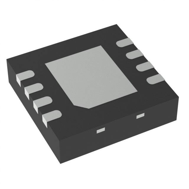
SON 8-pin Package with Thermal Pad
ESD Performance Tested per JESD 22
– 2000-V HBM and 1000-V CDM
Device Information(1)
PART NUMBER
TPS22975
TPS22975N
2 Applications
•
•
•
•
•
•
•
The TPS22975 is available in a small, space-saving
2-mm × 2-mm 8-pin SON package (DSG) with
integrated thermal pad allowing for high power
dissipation. The device is characterized for operation
over the free-air temperature range of –40°C to
+105°C.
PACKAGE
WSON (8)
BODY SIZE (NOM)
2.00 mm × 2.00 mm
(1) For all available packages, see the orderable addendum at
the end of the data sheet.
Ultrabook™
Notebooks and Netbooks
Tablet PC
Consumer Electronics
Set-top Boxes and Residential Gateways
Telecom Systems
Solid State Drives (SSDs)
On-Resistance vs Input Voltage
Simplified Schematic
40
35
ON
ON
CL
RL
CT
OFF
CT
GND
Power
Supply
GND
VBIAS
TPS22975
Copyright © 2016, Texas Instruments Incorporated
On-Resistance (m:)
C IN
-40 qC
25 qC
85 qC
105 qC
VOUT
VIN
Power
Supply
30
25
20
15
10
5
0
0.5
1
1.5
2
2.5
3
3.5
Input Voltage (V)
4
4.5
5
D007
VBIAS = 5 V, IVOUT = –200 mA
1
An IMPORTANT NOTICE at the end of this data sheet addresses availability, warranty, changes, use in safety-critical applications,
intellectual property matters and other important disclaimers. PRODUCTION DATA.
�TPS22975
SLVSDD0B – MAY 2016 – REVISED SEPTEMBER 2017
www.ti.com
Table of Contents
1
2
3
4
5
6
7
Features ..................................................................
Applications ...........................................................
Description .............................................................
Revision History.....................................................
Device Comparison Table.....................................
Pin Configuration and Functions .........................
Specifications.........................................................
7.1
7.2
7.3
7.4
7.5
7.6
7.7
7.8
7.9
8
9
1
1
1
2
3
3
4
Absolute Maximum Ratings ...................................... 4
ESD Ratings.............................................................. 4
Recommended Operating Conditions....................... 4
Thermal Information .................................................. 5
Electrical Characteristics—VBIAS = 5 V ..................... 5
Electrical Characteristics—VBIAS = 2.5 V .................. 6
Switching Characteristics .......................................... 7
Typical DC Characteristics........................................ 8
Typical AC Characteristics...................................... 10
Parameter Measurement Information ................ 13
Detailed Description ............................................ 14
9.1 Overview ................................................................. 14
9.2 Functional Block Diagram ....................................... 14
9.3 Feature Description................................................. 15
9.4 Device Functional Modes........................................ 15
10 Application and Implementation........................ 16
10.1 Application Information.......................................... 16
10.2 Typical Application ................................................ 16
11 Power Supply Recommendations ..................... 18
12 Layout................................................................... 19
12.1 Layout Guidelines ................................................. 19
12.2 Layout Example .................................................... 19
12.3 Thermal Considerations ........................................ 19
13 Device and Documentation Support ................. 20
13.1
13.2
13.3
13.4
13.5
13.6
13.7
Device Support......................................................
Related Documentation.........................................
Receiving Notification of Documentation Updates
Community Resources..........................................
Trademarks ...........................................................
Electrostatic Discharge Caution ............................
Glossary ................................................................
20
20
20
20
20
20
20
14 Mechanical, Packaging, and Orderable
Information ........................................................... 20
4 Revision History
Changes from Revision A (June 2016) to Revision B
•
Updated VIH in Recommended Operating Conditions ............................................................................................................ 4
Changes from Original (May 2016) to Revision A
•
2
Page
Page
Changed device status from Product Preview to Production Data ....................................................................................... 1
Submit Documentation Feedback
Copyright © 2016–2017, Texas Instruments Incorporated
Product Folder Links: TPS22975
�TPS22975
www.ti.com
SLVSDD0B – MAY 2016 – REVISED SEPTEMBER 2017
5 Device Comparison Table
DEVICE
RON AT VIN = VBIAS = 5 V
(TYPICAL)
QUICK-OUTPUT
DISCHARGE
MAXIMUM OUTPUT
CURRENT
ENABLE
TPS22975
16 mΩ
Yes
6A
Active high
TPS22975N
16 mΩ
No
6A
Active high
6 Pin Configuration and Functions
DSG Package
8-Pin (WSON)
Top View
DSG Package
8-Pin (WSON)
Bottom View
VIN
1
8
VOUT
VOUT
8
1
VIN
VIN
2
7
VOUT
VOUT
7
2
VIN
ON
3
6
CT
CT
6
3
ON
VBIAS
4
5
GND
GND
5
4
VBIAS
Pin Functions
PIN
I/O
DESCRIPTION
VIN
I
Switch input. Input bypass capacitor recommended for minimizing VIN dip. Must be connected to
Pin 1 and Pin 2. See the Application and Implementation section for more information
3
ON
I
Active high switch control input. Do not leave floating
4
VBIAS
I
Bias voltage. Power supply to the device. Recommended voltage range for this pin is 2.5 V to
5.7 V. See the Application and Implementation section for more information
5
GND
—
Device ground
6
CT
O
Switch slew rate control. Can be left floating. See the Adjustable Rise Time section under
Feature Description for more information
VOUT
O
Switch output
Thermal Pad
—
Thermal pad (exposed center pad) to alleviate thermal stress. Tie to GND. See the Layout
Example section for layout guidelines
NO.
1
2
7
8
—
NAME
Submit Documentation Feedback
Copyright © 2016–2017, Texas Instruments Incorporated
Product Folder Links: TPS22975
3
�TPS22975
SLVSDD0B – MAY 2016 – REVISED SEPTEMBER 2017
www.ti.com
7 Specifications
7.1 Absolute Maximum Ratings
Over operating free-air temperature range (unless otherwise noted) (1)
MIN
MAX
UNIT
VIN
Input voltage
–0.3
6
V
VOUT
Output voltage
–0.3
6
V
VBIAS
Bias voltage
–0.3
6
V
VON
On voltage
–0.3
6
V
IMAX
Maximum continuous switch current
6
A
IPLS
Maximum pulsed switch current, pulse < 300 µs, 2% duty cycle
8
A
TJ
Maximum junction temperature
125
°C
Tstg
Storage temperature
150
°C
(1)
–65
Stresses beyond those listed under Absolute Maximum Ratings may cause permanent damage to the device. These are stress ratings
only, which do not imply functional operation of the device at these or any other conditions beyond those indicated under Recommended
Operating Conditions. Exposure to absolute-maximum-rated conditions for extended periods may affect device reliability.
7.2 ESD Ratings
VALUE
V(ESD)
(1)
(2)
Electrostatic discharge
Human-body model (HBM), per ANSI/ESDA/JEDEC JS-001 (1)
±2000
Charged-device model (CDM), per JEDEC specification JESD22-C101 (2)
±1000
UNIT
V
JEDEC document JEP155 states that 500-V HBM allows safe manufacturing with a standard ESD control process.
JEDEC document JEP157 states that 250-V CDM allows safe manufacturing with a standard ESD control process.
7.3 Recommended Operating Conditions
MIN
MAX
UNIT
VIN
Input voltage
0.6
VBIAS
V
VBIAS
Bias voltage
2.5
5.7
V
VON
ON voltage
0
5.7
V
VOUT
Output voltage
VIN
V
VBIAS = 2.5 V to 5 V, TA< 85°C
1.05
5.7
VBIAS = 2.5 V to 5 V, TA< 105°C
1.1
5.7
VBIAS = 5 V to 5.7 V, TA< 105°C
1.2
5.7
0
0.5
VIH
High-level input voltage, ON
VIL
Low-level input voltage, ON
CIN
Input capacitor
1 (1)
TA
Operating free-air temperature (1) (2)
–40
(1)
(2)
4
VBIAS = 2.5 V to 5.7 V
V
V
µF
105
°C
See the Application Information section.
In applications where high power dissipation and-or poor package thermal resistance is present, the maximum ambient temperature may
have to be derated and device lifetime may be affected. Maximum ambient temperature (TA(max)) is dependent on the maximum
operating junction temperature (TJ(max)), the maximum power dissipation of the device in the application (PD(max)), and the junction-toambient thermal resistance of the part-package in the application (θJA), and can be approximated by the following equation: TA (max) =
TJ(max) – (θJA × PD(max)).
Submit Documentation Feedback
Copyright © 2016–2017, Texas Instruments Incorporated
Product Folder Links: TPS22975
�TPS22975
www.ti.com
SLVSDD0B – MAY 2016 – REVISED SEPTEMBER 2017
7.4 Thermal Information
TPS22975
THERMAL METRIC (1)
DSG (WSON)
UNIT
8 PINS
RθJA
Junction-to-ambient thermal resistance
RθJC(top)
Junction-to-case (top) thermal resistance
RθJB
Junction-to-board thermal resistance
ψJT
Junction-to-top characterization parameter
3.9
°C/W
ψJB
Junction-to-board characterization parameter
45.1
°C/W
RθJC(bot)
Junction-to-case (bottom) thermal resistance
16.4
°C/W
(1)
74.8
°C/W
81
°C/W
44.7
°C/W
For more information about traditional and new thermal metrics, see the Semiconductor and IC Package Thermal Metrics application
report.
7.5 Electrical Characteristics—VBIAS = 5 V
Unless otherwise noted, the specifications in the following table applies where VBIAS = 5 V. Typical values are for TA = 25 °C.
PARAMETER
TEST CONDITIONS
TA
MIN
TYP
MAX
UNIT
37
45
µA
2.3
µA
POWER SUPPLIES AND CURRENTS
IQ,
VBIAS
ISD,
VBIAS
VBIAS quiescent current
IOUT = 0 A,
VIN = VON = 5 V
–40°C to +105°C
VBIAS shutdown current
VON = VOUT = 0 V
–40°C to +105°C
VIN = 5 V
VIN = 3.3 V
ISD,
VIN
VIN off-state supply current
VON = VOUT = 0 V
VIN = 1.8 V
VIN = 0.6 V
ION
On-pin input leakage current
VON = 5.5 V
–40°C to +85°C
0.005
5
0.002
1.5
–40°C to +105°C
–40°C to +85°C
10
–40°C to +105°C
–40°C to +85°C
3.5
0.002
1
0.001
0.5
–40°C to +105°C
–40°C to +85°C
µA
2
–40°C to +105°C
1
–40°C to +105°C
0.1
µA
RESISTANCE CHARACTERISTICS
25°C
VIN = 5 V
16
–40°C to +85°C
23
–40°C to +105°C
25°C
VIN = 3.3 V
25
16
–40°C to +85°C
VIN = 1.8 V
RON
On-resistance
25
16
–40°C to +85°C
25°C
VIN = 1.5 V
25
16
–40°C to +85°C
VIN = 1.05 V
19
23
–40°C to +105°C
25
16
–40°C to +85°C
19
23
–40°C to +105°C
VON,
mΩ
25
16
–40°C to +85°C
25°C
VIN = 0.6 V
19
23
–40°C to +105°C
25°C
19
23
–40°C to +105°C
IOUT = –200 mA
19
23
–40°C to +105°C
25°C
19
25
HYS
On-pin hysteresis
VIN = 5 V
(1)
Output pulldown resistance
VIN = 5 V, VON = 0 V
TSD
Thermal shutdown
Junction temperature rising
160
°C
TSD, HYS
Thermal shutdown hysteresis
Junction temperature falling
20
°C
RPD
(1)
25°C
120
–40°C to +105°C
230
mV
300
Ω
TPS22975 only
Submit Documentation Feedback
Copyright © 2016–2017, Texas Instruments Incorporated
Product Folder Links: TPS22975
5
�TPS22975
SLVSDD0B – MAY 2016 – REVISED SEPTEMBER 2017
www.ti.com
7.6 Electrical Characteristics—VBIAS = 2.5 V
Unless otherwise noted, the specifications in the following table applies where VBIAS = 2.5 V. Typical values are for TA = 25
°C.
PARAMETER
TEST CONDITIONS
TA
MIN
TYP
MAX
UNIT
14
20
µA
1
µA
0.005
1.3
POWER SUPPLIES AND CURRENTS
IQ,
VBIAS
ISD,
VBIAS
VBIAS quiescent current
IOUT = 0 mA,
VIN = VON = 2.5 V
–40°C to +105°C
VBIAS shutdown current
VON = VOUT = 0 V
–40°C to +105°C
VIN = 2.5 V
VIN = 1.8 V
ISD,
VIN
VIN off-state supply current
VON = VOUT = 0 V
VIN = 1.05 V
VIN = 0.6 V
ION
On-pin input leakage current
VON = 5.5 V
–40°C to +85°C
–40°C to +105°C
–40°C to +85°C
2.6
0.002
1
0.002
0.8
–40°C to +105°C
–40°C to +85°C
2
–40°C to +105°C
–40°C to +85°C
µA
1.5
0.001
0.5
–40°C to +105°C
1
–40°C to +105°C
0.1
µA
RESISTANCE CHARACTERISTICS
25°C
VIN = 2.5 V
20
–40°C to +85°C
32
–40°C to +105°C
25°C
VIN = 1.8 V
34
18
–40°C to +85°C
RON
On-resistance
IOUT = –200 mA
VIN = 1.5 V
31
18
28
–40°C to +105°C
30
17
–40°C to +85°C
25°C
22
29
17
–40°C to +85°C
21
26
–40°C to +105°C
VON,
mΩ
27
–40°C to +105°C
VIN = 0.6 V
22
–40°C to +85°C
25°C
VIN = 1.2 V
23
29
–40°C to +105°C
25°C
26
27
On-pin hysteresis
VIN = 2.5 V
RPD (1)
Output pulldown resistance
VIN = 2.5 V, VON = 0 V
TSD
Thermal shutdown
Junction temperature rising
160
°C
TSD, HYS
Thermal shutdown hysteresis
Junction temperature falling
20
°C
(1)
6
HYS
25°C
85
–40°C to +105°C
230
mV
330
Ω
TPS22975 only
Submit Documentation Feedback
Copyright © 2016–2017, Texas Instruments Incorporated
Product Folder Links: TPS22975
�TPS22975
www.ti.com
SLVSDD0B – MAY 2016 – REVISED SEPTEMBER 2017
7.7 Switching Characteristics
PARAMETER
TEST CONDITION
MIN
TYP MAX
UNIT
VIN = VBIAS = 5 V, TA = 25ºC (unless otherwise noted)
tON
Turnon time
RL = 10 Ω, CL = 0.1 µF, CIN = 1 µF, CT = 1000 pF, VON = 5 V
1450
tOFF
Turnoff time
RL = 10 Ω, CL = 0.1 µF, CIN = 1 µF, CT = 1000 pF, VON = 5 V
2
tR
VOUT rise time
RL = 10 Ω, CL = 0.1 µF, CIN = 1 µF, CT = 1000 pF, VON = 5 V
1750
tF
VOUT fall time
RL = 10 Ω, CL = 0.1 µF, CIN = 1 µF, CT = 1000 pF, VON = 5 V
2
tD
ON delay time
RL = 10 Ω, CL = 0.1 µF, CIN = 1 µF, CT = 1000 pF, VON = 5 V
600
µs
VIN = 0.6 V, VBIAS = 5 V, TA = 25ºC (unless otherwise noted)
tON
Turnon time
RL = 10 Ω, CL = 0.1 µF, CIN = 1 µF, CT = 1000 pF, VON = 5 V
620
tOFF
Turnoff time
RL = 10 Ω, CL = 0.1 µF, CIN = 1 µF, CT = 1000 pF, VON = 5 V
2
tR
VOUT rise time
RL = 10 Ω, CL = 0.1 µF, CIN = 1 µF, CT = 1000 pF, VON = 5 V
280
tF
VOUT fall time
RL = 10 Ω, CL = 0.1 µF, CIN = 1 µF, CT = 1000 pF, VON = 5 V
2
tD
ON delay time
RL = 10 Ω, CL = 0.1 µF, CIN = 1 µF, CT = 1000 pF, VON = 5 V
485
µs
VIN = VBIAS = 2.5 V, TA = 25ºC (unless otherwise noted)
tON
Turnon time
RL = 10 Ω, CL = 0.1 µF, CIN = 1 µF, CT = 1000 pF, VON = 5 V
tOFF
Turnoff time
RL = 10 Ω, CL = 0.1 µF, CIN = 1 µF, CT = 1000 pF, VON = 5 V
2180
2
tR
VOUT rise time
RL = 10 Ω, CL = 0.1 µF, CIN = 1 µF, CT = 1000 pF, VON = 5 V
2150
tF
VOUT fall time
RL = 10 Ω, CL = 0.1 µF, CIN = 1 µF, CT = 1000 pF, VON = 5 V
2
tD
ON delay time
RL = 10 Ω, CL = 0.1 µF, CIN = 1 µF, CT = 1000 pF, VON = 5 V
1120
µs
VIN = 0.6 V, VBIAS = 2.5 V, TA = 25ºC (unless otherwise noted)
tON
Turnon time
RL = 10 Ω, CL = 0.1 µF, CIN = 1 µF, CT = 1000 pF, VON = 5 V
tOFF
Turnoff time
RL = 10 Ω, CL = 0.1 µF, CIN = 1 µF, CT = 1000 pF, VON = 5 V
1315
3
tR
VOUT rise time
RL = 10 Ω, CL = 0.1 µF, CIN = 1 µF, CT = 1000 pF, VON = 5 V
650
tF
VOUT fall time
RL = 10 Ω, CL = 0.1 µF, CIN = 1 µF, CT = 1000 pF, VON = 5 V
2
tD
ON delay time
RL = 10 Ω, CL = 0.1 µF, CIN = 1 µF, CT = 1000 pF, VON = 5 V
975
Submit Documentation Feedback
Copyright © 2016–2017, Texas Instruments Incorporated
Product Folder Links: TPS22975
µs
7
�TPS22975
SLVSDD0B – MAY 2016 – REVISED SEPTEMBER 2017
www.ti.com
7.8 Typical DC Characteristics
70
-40 qC
25 qC
85 qC
105 qC
50
VBIAS Quiescent Current (PA)
VBIAS Quiescent Current (PA)
60
40
30
20
10
2.5
3
3.5
VIN = VBIAS
4
4.5
Bias Voltage (V)
5
60
50
40
30
20
10
0.5
5.5
VON = 5 V
VOUT = 0 V
1.5
2
VBIAS = 5 V
Figure 1. VBIAS Quiescent Current vs Bias Voltage
2.5
3
3.5
Input Voltage (V)
4
4.5
5
D002
VON = 5 V
VOUT = 0 V
Figure 2. VBIAS Quiescent Current vs Input Voltage
0.8
-40 qC
25 qC
85 qC
105 qC
2
VIN Off-State Supply Current (PA)
VBIAS Shutdown Current (PA)
1
D001
2.5
1.5
1
0.5
0
2.5
-40 qC
25 qC
85 qC
105 qC
0.7
0.6
0.5
0.4
0.3
0.2
0.1
0
3
3.5
VIN = VBIAS
4
4.5
Bias Voltage (V)
5
5.5
6
0
0.5
1
1.5
D003
VON = 0 V
VOUT = 0 V
VBIAS = 5 V
Figure 3. VBIAS Shutdown Current vs Bias Voltage
2
2.5
3
Input Voltage (V)
3.5
4
4.5
5
D001
D004
VON = 0 V
VOUT = 0 V
Figure 4. VIN Off-State Supply Current vs Input Voltage
30
30
VIN = 0.6 V
VIN = 3.3 V
VIN = 5 V
VIN = 0.6 V
VIN = 1.8 V
VIN = 2.5 V
25
On-Resistance (m:)
25
On-Resistance (m:)
-40 qC
25 qC
85 qC
105 qC
20
15
10
5
20
15
10
5
0
-40
-10
VBIAS = 5 V
Note:
20
50
Ambient Temperature (qC)
80
110
0
-40
-10
D005
IOUT = –200 mA
VON = 5 V
All three RON curves have the same
values; therefore, only one line is visible.
VBIAS = 2.5 V
20
50
Ambient Temperature (qC)
IOUT = –200 mA
80
110
D006
VON = 5 V
Figure 6. On-Resistance vs Ambient Temperature
Figure 5. On-Resistance vs Ambient Temperature
8
Submit Documentation Feedback
Copyright © 2016–2017, Texas Instruments Incorporated
Product Folder Links: TPS22975
�TPS22975
www.ti.com
SLVSDD0B – MAY 2016 – REVISED SEPTEMBER 2017
Typical DC Characteristics (continued)
40
40
-40 qC
25 qC
85 qC
105 qC
30
-40 qC
25 qC
85 qC
105 qC
35
On-Resistance (m:)
On-Resistance (m:)
35
25
20
15
10
5
30
25
20
15
10
5
0
0.5
1
1.5
2
VBIAS = 5 V
2.5
3
3.5
Input Voltage (V)
4
4.5
0
0.5
5
IOUT = –200 mA
VON = 5 V
Figure 7. On-Resistance vs Input Voltage
2
2.5
D009
D008
IOUT = –200 mA
VON = 5 V
Figure 8. On-Resistance vs Input Voltage
275
Output Pull Down Resistence (:)
VIN = 0.6 V
VIN = 1.2 V
VIN = 1.8 V
VIN = 2.5 V
20
On-Resistance (m:)
1.5
Input Voltage (V)
VBIAS = 2.5 V
25
15
10
5
0
2.5
1
D007
3
TA = 25°C
3.5
4
4.5
Bias Voltage (V)
5
IOUT = –200 mA
5.5
6
-40°C
25°C
85°C
105°C
270
265
260
255
250
245
240
235
2.5
3
D009
VON = 5 V
Figure 9. On-Resistance vs Bias Voltage
VIN = 2.5 V
3.5
4
4.5
Bias Voltage (V)
5
5.5
6
D001
VON = 0 V
Figure 10. Output Pull Down Resistance vs Bias Voltage
Submit Documentation Feedback
Copyright © 2016–2017, Texas Instruments Incorporated
Product Folder Links: TPS22975
9
�TPS22975
SLVSDD0B – MAY 2016 – REVISED SEPTEMBER 2017
www.ti.com
7.9 Typical AC Characteristics
TA = 25°C, CT = 1000 pF, CIN = 1 µF, CL = 0.1 µF, RL = 10 Ω
900
1700
Delay Time (us)
Delay Time (us)
1500
-40 qC
25 qC
85 qC
105 qC
-40 qC
25 qC
85 qC
105 qC
1300
1100
700
500
900
700
0.5
1
1.5
Input Voltage (V)
2
300
0.5
2.5
VBIAS = 2.5 V
4
4.5
5
D012
-40 qC
25 qC
85 qC
105 qC
2.3
Fall Time (us)
Fall Time (us)
2.5
3
3.5
Input Voltage (V)
2.5
-40 qC
25 qC
85 qC
105 qC
2.1
1.9
1.7
2.1
1.9
1.7
1.5
0.5
1
1.5
Input Voltage (V)
2
1.5
0.5
2.5
1
1.5
2
D013
VBIAS = 2.5 V
2.5
3
3.5
Input Voltage (V)
4
4.5
5
D014
VBIAS = 5 V
Figure 13. Fall Time vs Input Voltage
Figure 14. Fall Time vs Input Voltage
2.4
3.3
-40 qC
25 qC
85 qC
105 qC
3.2
3.1
-40 qC
25 qC
85 qC
105 qC
2.3
2.2
Turnoff Time (us)
3
Turnoff Time (us)
2
Figure 12. Delay Time vs Input Voltage
2.5
2.9
2.8
2.7
2.6
2.5
2.4
2.1
2
1.9
1.8
2.3
1.7
2.2
2.1
0.5
1
1.5
Input Voltage (V)
2
2.5
1.6
0.5
1
1.5
D015
VBIAS = 2.5 V
2
2.5
3
3.5
Input Voltage (V)
4
4.5
5
D016
VBIAS = 5 V
Figure 15. Turnoff Time vs Input Voltage
10
1.5
VBIAS = 5 V
Figure 11. Delay Time vs Input Voltage
2.3
1
D011
Submit Documentation Feedback
Figure 16. Turnoff Time vs Input Voltage
Copyright © 2016–2017, Texas Instruments Incorporated
Product Folder Links: TPS22975
�TPS22975
www.ti.com
SLVSDD0B – MAY 2016 – REVISED SEPTEMBER 2017
Typical AC Characteristics (continued)
TA = 25°C, CT = 1000 pF, CIN = 1 µF, CL = 0.1 µF, RL = 10 Ω
2000
3000
-40 qC
25 qC
85 qC
105 qC
-40 qC
25 qC
85 qC
105 qC
1600
Turnon Time (us)
Turnon Time (us)
2500
2000
1500
1000
1200
800
400
500
0
0.5
1
1.5
Input Voltage (V)
2
0
0.5
2.5
VBIAS = 2.5 V
1.5
2
2.5
3
3.5
Input Voltage (V)
4
4.5
5
D018
VBIAS = 5 V
Figure 17. Turnon Time vs Input Voltage
Figure 18. Turnon Time vs Input Voltage
3000
2500
-40 qC
25 qC
85 qC
105 qC
2500
-40 qC
25 qC
85 qC
105 qC
2000
2000
Rise Time (us)
Rise Time (us)
1
D017
1500
1000
1500
1000
500
500
0
0.5
1
1.5
Input Voltage (V)
2
2.5
0
0.5
VBIAS = 2.5 V
1.5
2
2.5
3
3.5
Input Voltage (V)
4
4.5
5
D020
VBIAS = 5 V
Figure 19. Rise Time vs Input Voltage
VIN = 0.6 V
1
D019
VBIAS = 2.5 V
Figure 20. Rise Time vs Input Voltage
VIN = 0.6 V
Figure 21. Turnon Response Time
VBIAS = 5 V
Figure 22. Turnon Response Time
Submit Documentation Feedback
Copyright © 2016–2017, Texas Instruments Incorporated
Product Folder Links: TPS22975
11
�TPS22975
SLVSDD0B – MAY 2016 – REVISED SEPTEMBER 2017
www.ti.com
Typical AC Characteristics (continued)
TA = 25°C, CT = 1000 pF, CIN = 1 µF, CL = 0.1 µF, RL = 10 Ω
VIN = 2.5 V
VBIAS = 2.5 V
VIN = 5 V
Figure 23. Turnon Response Time
VIN = 0.6 V
VBIAS = 2.5 V
Figure 24. Turnon Response Time
VIN = 0.6 V
Figure 25. Turnoff Response Time
VIN = 2.5 V
VBIAS = 2.5 V
VBIAS = 5 V
Figure 26. Turnoff Response Time
VIN = 5 V
Figure 27. Turnoff Response Time
12
VBIAS = 5 V
Submit Documentation Feedback
VBIAS = 5 V
Figure 28. Turnoff Response Time
Copyright © 2016–2017, Texas Instruments Incorporated
Product Folder Links: TPS22975
�TPS22975
www.ti.com
SLVSDD0B – MAY 2016 – REVISED SEPTEMBER 2017
8 Parameter Measurement Information
VOUT
VIN
Power
Supply
ON
C IN
ON
CL
RL
CT
OFF
CT
GND
Power
Supply
GND
VBIAS
TPS22975
Copyright © 2016, Texas Instruments Incorporated
A.
Rise and fall times of the control signal are 100 ns.
B.
Turnoff times and fall times are dependent on the time constant at the load. For the TPS22975, the internal pull-down
resistance RPD is enabled when the switch is disabled. The time constant is (RPD || RL) × CL.
Figure 29. Test Circuit
VON
50%
50%
tOFF
tON
VOUT
50%
50%
tF
tR
90%
VOUT
10%
10%
90%
10%
tD
Figure 30. tON and tOFF Waveforms
Submit Documentation Feedback
Copyright © 2016–2017, Texas Instruments Incorporated
Product Folder Links: TPS22975
13
�TPS22975
SLVSDD0B – MAY 2016 – REVISED SEPTEMBER 2017
www.ti.com
9 Detailed Description
9.1 Overview
The TPS22975 device is a single-channel, 6-A load switch in an 8-pin SON package. To reduce the voltage drop
in high current rails, the device implements an N-channel MOSFET. The device has a configurable slew rate for
applications that require a specific rise-time.
The device prevents downstream circuits from pulling high standby current from the supply by limiting the
leakage current of the device when it is disabled. The integrated control logic, driver, power supply, and output
discharge FET eliminates the need for any external components, which reduces solution size and bill of materials
(BOM) count.
9.2 Functional Block Diagram
VIN
Charge
Pump
VBIAS
ON
Control
Logic
VOUT
CT
TPS22975 Only
GND
Copyright © 2016, Texas Instruments Incorporated
14
Submit Documentation Feedback
Copyright © 2016–2017, Texas Instruments Incorporated
Product Folder Links: TPS22975
�TPS22975
www.ti.com
SLVSDD0B – MAY 2016 – REVISED SEPTEMBER 2017
9.3 Feature Description
9.3.1 Adjustable Rise Time
A capacitor to GND on the CT pin sets the slew rate. The voltage on the CT pin can be as high as 15 V;
therefore, the minimum voltage rating for the CT capacitor must be 30 V for optimal performance. An
approximate formula for the relationship between CT and slew rate when VBIAS is set to 5 V is shown in
Equation 1. This equation accounts for 10% to 90% measurement on VOUT and does not apply for CT < 100 pF.
Use Table 1 to determine rise times for when CT = 0 pF.
SR
0.43 u CT 26
where
•
•
•
SR is the slew rate (in µs/V)
CT is the capacitance value on the CT pin (in pF)
The units for the constant 26 are µs/V. The units for the constant 0.43 are µs/(V × pF).
(1)
Rise time can be calculated by multiplying the input voltage by the slew rate. Table 1 contains rise time values
measured on a typical device. Rise times shown in Table 1 are only valid for the power-up sequence where VIN
and VBIAS are already in steady state condition before the ON pin is asserted high.
Table 1. Rise Time tR vs CT Capacitor
CT (pF)
(1)
RISE TIME (µs) 10% - 90%, CL = 0.1 µF, CIN = 1 µF, RL = 10 Ω, VBIAS = 5 V (1)
VIN = 5 V
VIN = 3.3 V
VIN = 1.8 V
VIN = 1.5 V
VIN = 1.2 V
VIN = 1.05 V
VIN = 0.6 V
0
140
105
75
65
60
55
40
220
520
360
215
185
160
140
95
470
970
660
385
330
275
240
155
1000
1750
1190
700
595
495
435
275
2200
3875
2615
1520
1290
1070
940
595
4700
7580
5110
2950
2510
2075
1830
1150
10000
16980
11485
6650
5635
4685
4110
2595
Typical Values at 25°C with a 25-V X7R 10% Ceramic Capacitor on CT
9.3.2 Quick-Output Discharge (QOD) (Optional)
The TPS22975 includes an optional QOD feature. When the switch is disabled, an internal discharge resistance
is connected between VOUT and GND to remove the remaining charge from the output. This resistance has a
typical value of 230 Ω and prevents the output from floating while the switch is disabled. For best results, it is
recommended that the device gets disabled before VBIAS falls below the minimum recommended voltage.
9.3.3 Thermal Shutdown
Thermal shutdown protects the part from internally or externally generated excessive temperatures. When the
device temperature triggers TSD (typical 160°C), the switch is turned off. The switch automatically turns on again
if the temperature of the die drops 20 degrees below the TSD threshold.
9.4 Device Functional Modes
The Table 2 lists the VOUT pin states as determined by the ON pin.
Table 2. VOUT Connection
ON
TPS22975
TPS22975N
L
GND
Open
H
VIN
VIN
Submit Documentation Feedback
Copyright © 2016–2017, Texas Instruments Incorporated
Product Folder Links: TPS22975
15
�TPS22975
SLVSDD0B – MAY 2016 – REVISED SEPTEMBER 2017
www.ti.com
10 Application and Implementation
NOTE
Information in the following applications sections is not part of the TI component
specification, and TI does not warrant its accuracy or completeness. TI’s customers are
responsible for determining suitability of components for their purposes. Customers should
validate and test their design implementation to confirm system functionality.
10.1 Application Information
10.1.1 ON and OFF Control
The ON pin controls the state of the switch. ON is active high and has a 1.2-V ON-pin enable threshold, making
it capable of interfacing with low-voltage signals. The ON pin is compatible with standard GPIO logic thresholds.
It can be used with any microcontroller with 1.2 V or higher GPIO voltage. This pin cannot be left floating and
must be driven either high or low for proper functionality.
10.1.2 Input Capacitor (CIN) (Optional)
To limit the voltage drop on the input supply caused by transient inrush currents when the switch turns on into a
discharged load capacitor or short-circuit, a capacitor needs to be placed between VIN and GND. A 1-µF ceramic
capacitor, CIN, placed close to the pins, is usually sufficient. Higher values of CIN can be used to further reduce
the voltage drop during high current applications. When switching heavy loads, it is recommended to have an
input capacitor about 10 times higher than the output capacitor (CL) to avoid excessive voltage drop.
10.1.3 Output Capacitor (CL) (Optional)
Because of the integrated body diode in the NMOS switch, a CIN greater than CL is highly recommended. A CL
greater than CIN can cause VOUT to exceed VIN when the system supply is removed. This could result in current
flow through the body diode from VOUT to VIN. A CIN to CL ratio of 10 to 1 is recommended for minimizing VIN dip
caused by inrush currents during startup; however, a 10 to 1 ratio for capacitance is not required for proper
functionality of the device. A ratio smaller than 10 to 1 (such as 1 to 1) could cause slightly more VIN dip upon
turn-on because of inrush currents. This can be mitigated by increasing the capacitance on the CT pin for a
longer rise time (see the Adjustable Rise Time section).
10.2 Typical Application
For optimal RON performance, it is recommended to have VIN ≤ VBIAS. The device is functional if VIN > VBIAS but it
exhibits RON greater than what is listed in the Electrical Characteristics—VBIAS = 5 V and Electrical
Characteristics—VBIAS = 2.5 V tables.
Figure 31 demonstrates how the TPS22975 can be used to power downstream modules.
VOUT
VIN
Power
Supply
ON
C IN
ON
CL
RL
CT
OFF
CT
GND
Power
Supply
GND
VBIAS
TPS22975
Copyright © 2016, Texas Instruments Incorporated
Figure 31. Powering a Downstream Module
16
Submit Documentation Feedback
Copyright © 2016–2017, Texas Instruments Incorporated
Product Folder Links: TPS22975
�TPS22975
www.ti.com
SLVSDD0B – MAY 2016 – REVISED SEPTEMBER 2017
Typical Application (continued)
10.2.1 Design Requirements
DESIGN PARAMETER
EXAMPLE VALUE
VIN
3.3 V
VBIAS
5V
CL
22 µF
Maximum Acceptable Inrush Current
400 mA
10.2.2 Detailed Design Procedure
10.2.2.1 Inrush Current
When the switch is enabled, the output capacitors must be charged up from 0 V to the set value (3.3 V in this
example). This charge arrives in the form of inrush current. Inrush current can be calculated using Equation 2.
Inrush Current = CL × dVOUT/dt
Where:
•
•
•
CL is the output capacitance
dVOUT is the change in VOUT during the ramp up of the output voltage when device is enabled.
dt is the rise time in VOUT during the ramp up of the output voltage when the device is enabled.
(2)
The TPS22975 offers adjustable rise time for VOUT. This feature allows the user to control the inrush current
during turnon. The appropriate rise time can be calculated using the design requirements and the inrush current
equation as shown in Equation 3.
400 mA = 22 µF × 3.3 V/dt
(3)
The value of dt is given by Equation 4.
dt = 181.5 µs
(4)
To ensure an inrush current of less than 400 mA, choose a CT value that yields a rise time of more than 181.5
µs. See the oscilloscope captures in the Application Curves section for an example of how the CT capacitor can
be used to reduce inrush current.
10.2.3 Application Curves
VBIAS = 5 V
VIN = 3.3 V
CL = 22 µF
Figure 32. Inrush Current with CT = 0 pF
VBIAS = 5 V
VIN = 3.3 V
CL = 22 µF
Figure 33. Inrush Current with CT = 220 pF
Submit Documentation Feedback
Copyright © 2016–2017, Texas Instruments Incorporated
Product Folder Links: TPS22975
17
�TPS22975
SLVSDD0B – MAY 2016 – REVISED SEPTEMBER 2017
www.ti.com
11 Power Supply Recommendations
The supply to the device must be well regulated and placed as close to the device terminal as possible with the
recommended 1-μF bypass capacitor. If the supply is located more than a few inches from the device terminals,
additional bulk capacitance may be required in addition to the ceramic bypass capacitors. If additional bulk
capacitance is required, an electrolytic, tantalum or ceramic capacitor of 1 μF may be sufficient.
The TPS22975 operates regardless of power sequencing order. The order in which voltages are applied to VIN,
VBIAS, and ON does not damage the device as long as the voltages do not exceed the absolute maximum
operating conditions. If voltage is applied to ON before VIN, the slew rate of VOUT can not be controlled.
18
Submit Documentation Feedback
Copyright © 2016–2017, Texas Instruments Incorporated
Product Folder Links: TPS22975
�TPS22975
www.ti.com
SLVSDD0B – MAY 2016 – REVISED SEPTEMBER 2017
12 Layout
12.1 Layout Guidelines
For best performance, all traces must be as short as possible. To be most effective, the input and output
capacitors must be placed close to the device to minimize the effects that parasitic trace inductances may have
on normal operation. Using wide traces for VIN, VOUT, and GND helps minimize the parasitic electrical effects
along with minimizing the case to ambient thermal impedance. The CT trace must be as short as possible to
reduce parasitic capacitance.
12.2 Layout Example
VIA to GND
Pin 1
VIN
(1)
VIN
VOUT
VOUT
GND
CT
ON
GND
VBIAS
Figure 34. Layout Recommendation
12.3 Thermal Considerations
The maximum IC junction temperature must be restricted to 125°C under normal operating conditions. To
calculate the maximum allowable dissipation, PD(max) , for a given ambient temperature, use Equation 5 as a
guideline.
PD(max) =
TJ(max) - TA
θJA
where
•
•
•
•
PD(max) is the maximum allowable power dissipation
TJ(max) is the maximum allowable junction temperature (125°C for the TPS22975)
TA is the ambient temperature of the device
ΘJA is the junction to air thermal impedance. See the Thermal Information section. This parameter is highly
dependent upon board layout.
(5)
In Figure 34, notice that the thermal vias are located under the exposed thermal pad of the device. This allows
for thermal diffusion away from the device.
Submit Documentation Feedback
Copyright © 2016–2017, Texas Instruments Incorporated
Product Folder Links: TPS22975
19
�TPS22975
SLVSDD0B – MAY 2016 – REVISED SEPTEMBER 2017
www.ti.com
13 Device and Documentation Support
13.1 Device Support
13.1.1 Developmental Support
For the TPS22975 PSpice Transient Model, see SLVMBO6.
13.2 Related Documentation
For related documentation see the following:
• Fundamentals of On-Resistance in Load Switches, SLVA771
• TPS22975 Load Switch Evaluation Module User's Guide, SLVUAR3
13.3 Receiving Notification of Documentation Updates
To receive notification of documentation updates, navigate to the device product folder on ti.com. In the upper
right corner, click on Alert me to register and receive a weekly digest of any product information that has
changed. For change details, review the revision history included in any revised document.
13.4 Community Resources
The following links connect to TI community resources. Linked contents are provided "AS IS" by the respective
contributors. They do not constitute TI specifications and do not necessarily reflect TI's views; see TI's Terms of
Use.
TI E2E™ Online Community TI's Engineer-to-Engineer (E2E) Community. Created to foster collaboration
among engineers. At e2e.ti.com, you can ask questions, share knowledge, explore ideas and help
solve problems with fellow engineers.
Design Support TI's Design Support Quickly find helpful E2E forums along with design support tools and
contact information for technical support.
13.5 Trademarks
E2E is a trademark of Texas Instruments.
Ultrabook is a trademark of Intel.
All other trademarks are the property of their respective owners.
13.6 Electrostatic Discharge Caution
This integrated circuit can be damaged by ESD. Texas Instruments recommends that all integrated circuits be handled with
appropriate precautions. Failure to observe proper handling and installation procedures can cause damage.
ESD damage can range from subtle performance degradation to complete device failure. Precision integrated circuits may be more
susceptible to damage because very small parametric changes could cause the device not to meet its published specifications.
13.7 Glossary
SLYZ022 — TI Glossary.
This glossary lists and explains terms, acronyms, and definitions.
14 Mechanical, Packaging, and Orderable Information
The following pages include mechanical, packaging, and orderable information. This information is the most
current data available for the designated devices. This data is subject to change without notice and revision of
this document. For browser-based versions of this data sheet, refer to the left-hand navigation.
20
Submit Documentation Feedback
Copyright © 2016–2017, Texas Instruments Incorporated
Product Folder Links: TPS22975
�PACKAGE OPTION ADDENDUM
www.ti.com
22-Nov-2022
PACKAGING INFORMATION
Orderable Device
Status
(1)
Package Type Package Pins Package
Drawing
Qty
Eco Plan
(2)
Lead finish/
Ball material
MSL Peak Temp
Op Temp (°C)
Device Marking
(3)
Samples
(4/5)
(6)
TPS22975DSGR
ACTIVE
WSON
DSG
8
3000
RoHS & Green
NIPDAU
Level-1-260C-UNLIM
-40 to 105
13XH
Samples
TPS22975DSGT
ACTIVE
WSON
DSG
8
250
RoHS & Green
NIPDAU
Level-1-260C-UNLIM
-40 to 105
13XH
Samples
TPS22975NDSGR
ACTIVE
WSON
DSG
8
3000
RoHS & Green
NIPDAU
Level-1-260C-UNLIM
-40 to 105
14YH
Samples
TPS22975NDSGT
ACTIVE
WSON
DSG
8
250
RoHS & Green
NIPDAU
Level-1-260C-UNLIM
-40 to 105
14YH
Samples
(1)
The marketing status values are defined as follows:
ACTIVE: Product device recommended for new designs.
LIFEBUY: TI has announced that the device will be discontinued, and a lifetime-buy period is in effect.
NRND: Not recommended for new designs. Device is in production to support existing customers, but TI does not recommend using this part in a new design.
PREVIEW: Device has been announced but is not in production. Samples may or may not be available.
OBSOLETE: TI has discontinued the production of the device.
(2)
RoHS: TI defines "RoHS" to mean semiconductor products that are compliant with the current EU RoHS requirements for all 10 RoHS substances, including the requirement that RoHS substance
do not exceed 0.1% by weight in homogeneous materials. Where designed to be soldered at high temperatures, "RoHS" products are suitable for use in specified lead-free processes. TI may
reference these types of products as "Pb-Free".
RoHS Exempt: TI defines "RoHS Exempt" to mean products that contain lead but are compliant with EU RoHS pursuant to a specific EU RoHS exemption.
Green: TI defines "Green" to mean the content of Chlorine (Cl) and Bromine (Br) based flame retardants meet JS709B low halogen requirements of