Sample &
Buy
Product
Folder
Support &
Community
Tools &
Software
Technical
Documents
TPS22981
SLVSBM6B – DECEMBER 2012 – REVISED NOVEMBER 2015
TPS22981 3.3-V to 18-V Thunderbolt™ Power Mux
1 Features
3 Description
•
•
•
•
•
•
•
•
The TPS22981 device is a current-limited power mux
providing a connection to a peripheral device from
either a low-voltage supply (3 V to 3.6 V) or a highvoltage supply (4.5 V to 19.8 V). The desired output
is selected by digital control signals.
1
Powered from 3.3 V
4.5-V to 19.8-V High-Voltage Switch
3-V to 3.6-V Switch
Adjustable Current Limit
Thermal Shutdown
Make Before Break Switch
High-Voltage Discharge Before Low-Voltage Make
Reverse Current Blocking
2 Applications
•
•
•
Notebook Computers
Desktop Computers
Power Management Systems
Typical Application
OUT
HV_EN
GND
OUT
RSVD
connector
RSET_S0
ISET_S0
ENHVU
RSET_S3
ISET_S3
S0
RSET_V3P3
V3P3OUT
VHV
To prevent current backflow during a switch over from
a VHV connection to a V3P3 connection, the
TPS22981 will break the VHV connection, discharge
the output to approximately 3.3 V and then make the
V3P3 connection. The output may transition to 0 V
when a load is present, before returning to 3.3 V.
DC/DC
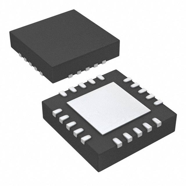
The TPS22981 is available in a 4 mm × 4 mm × 1
mm VQFN package.
Device Information(1)
EN
FAULTZ
V3P3
GND
VHV
GND
When the high-voltage supply is not present, the
TPS22981 will maintain the connection to the output
from the low-voltage supply. Upon the presence of a
high-voltage line and high-voltage enable signal, the
high-voltage switch is turned on in conjunction with
the low-voltage switch until a reverse current is
detected through the low-voltage switch, allowing a
seamless transition from low voltage to the highvoltage supply with minimal droop and shoot-through
current.
ISET_V3P3
V3P3
GND
DC/DC
Exposed Pad
The high-voltage (VHV) and low-voltage (V3P3)
switch current limits are set with external resistance.
Once the current limit is reached, the TPS22981 will
control the switch to maintain the current at this limit.
PART NUMBER
TPS22981
µC
PACKAGE
VQFN (20)
BODY SIZE (NOM)
4.00 mm × 4.00 mm
(1) For all available packages, see the orderable addendum at
the end of the data sheet.
1
An IMPORTANT NOTICE at the end of this data sheet addresses availability, warranty, changes, use in safety-critical applications,
intellectual property matters and other important disclaimers. PRODUCTION DATA.
�TPS22981
SLVSBM6B – DECEMBER 2012 – REVISED NOVEMBER 2015
www.ti.com
Table of Contents
1
2
3
4
5
6
7
Features ..................................................................
Applications ...........................................................
Description .............................................................
Revision History.....................................................
Pin Configuration and Functions .........................
Specifications.........................................................
1
1
1
2
3
4
6.1
6.2
6.3
6.4
6.5
6.6
4
4
4
5
5
6
Absolute Maximum Ratings ......................................
ESD Ratings..............................................................
Recommended Operating Conditions.......................
Thermal Information ..................................................
Electrical Characteristics...........................................
Dissipation Ratings ...................................................
Detailed Description .............................................. 7
7.1 Overview ................................................................... 7
7.2 Functional Block Diagram ......................................... 8
7.3 Feature Description................................................... 9
7.4 Device Functional Modes........................................ 13
8
Application and Implementation ........................ 15
8.1 Application Information............................................ 15
8.2 Typical Application ................................................. 15
9 Power Supply Recommendations...................... 16
10 Layout................................................................... 17
10.1 Layout Guidelines ................................................. 17
10.2 Layout Example .................................................... 18
11 Device and Documentation Support ................. 19
11.1
11.2
11.3
11.4
Community Resources..........................................
Trademarks ...........................................................
Electrostatic Discharge Caution ............................
Glossary ................................................................
19
19
19
19
12 Mechanical, Packaging, and Orderable
Information ........................................................... 19
4 Revision History
NOTE: Page numbers for previous revisions may differ from page numbers in the current version.
Changes from Revision A (September 2013) to Revision B
Page
•
Added Pin Configuration and Functions section, ESD Ratings table, Feature Description section, Device Functional
Modes, Application and Implementation section, Power Supply Recommendations section, Layout section, Device
and Documentation Support section, and Mechanical, Packaging, and Orderable Information section ............................... 1
•
Replaced all the equations links needed to calculate resistor values in the table to the correct equation, Equation 1......... 3
•
Changed V3P3OUT pinout 'capacitor' to 'capacitor to GND' throughout the data sheet ....................................................... 3
•
Added labels to all pins in the Functional Block Diagram ..................................................................................................... 8
•
Changed Input Inductive Bounce at Short Circuit section title to Input Inductive Bounce ................................................... 15
•
Updated Figure 9 to show the EN pin as a device input ...................................................................................................... 15
Changes from Original (December 2012) to Revision A
Page
•
Removed Ordering Information table. .................................................................................................................................... 3
•
Added ROUTDIS parameter to the Electrical Characteristics table............................................................................................ 5
•
Updated UVLO ENABLE section.......................................................................................................................................... 13
2
Submit Documentation Feedback
Copyright © 2012–2015, Texas Instruments Incorporated
Product Folder Links: TPS22981
�TPS22981
www.ti.com
SLVSBM6B – DECEMBER 2012 – REVISED NOVEMBER 2015
5 Pin Configuration and Functions
11
V3P3
S0
V3P3
V3P3OUT
V3P3OUT
V3P3
S0
V3P3
ENHVU
15
14
13
OUT
ENHVU
12
11
HV_EN
HV_EN
12
OUT
OUT
13
GND
GND
14
GND
OUT
15
RGP Package
VQFN With Exposed Thermal Pad
Bottom View
GND
GND
RGP Package
VQFN With Exposed Thermal Pad
Top View
Pin Functions
PIN
NAME
NO.
TYPE
DESCRIPTION
EN
5
I
Device active-high enable.
ENHVU
16
I
Enable VHV UVLO control of device enable. When asserted high, both V3P3 and VHV must be
present for device enable. When low, only V3P3 must be present for device enable.
FAULTZ
4
O
Fault condition output. This pin is an open-drain pulldown indicating a fault condition. Place a pullup
resistance (RFAULTZ) between this pin and V3P3. Float pin or tie pin to GND if unused.
GND
1, 2, 3,
13, 15
P
Device ground. All GND pins must be connected to board ground.
GND
EP
P
Exposed pad must be connected to device GND.
HV_EN
11
I
Active-high voltage output enable.
ISET_S0
10
I
Sets the current limit for VHV in S0 mode. Place resistor between this pin and GND. See Equation 1 to
calculate resistor value.
ISET_S3
9
I
Sets the current limit for VHV in S3 mode. Place resistor between this pin and GND. See Equation 1 to
calculate resistor value.
ISET_V3P
3
8
I
Sets the current limit for V3P3. Place resistor between this pin and GND. See Equation 1 to calculate
resistor value.
12, 14
O
Power output. Place a minimum of 1-µF capacitor to GND as close to this pin as possible.
17
I
When this pin is asserted, the device is put in S0 mode. Otherwise the device operates in S3 mode.
19, 20
P
3.3-V power supply input. Place a minimum of 0.1-µF capacitor to GND as close to this pin as
possible.
V3P3OUT
18
O
3.3-V bypass output. When ENHVU is low, this path is enabled by EN and the V3P3 UVLO. When
ENHVU is high, this path is enabled by EN and both the V3P3 UVLO and the VHV UVLO. Place a
minimum 0.1-uF capacitor to GND as close to this pin as possible.
VHV
6, 7
P
High voltage power supply input. See the Input Inductive Bounce section for more information.
OUT
S0
V3P3
Submit Documentation Feedback
Copyright © 2012–2015, Texas Instruments Incorporated
Product Folder Links: TPS22981
3
�TPS22981
SLVSBM6B – DECEMBER 2012 – REVISED NOVEMBER 2015
www.ti.com
6 Specifications
6.1 Absolute Maximum Ratings
over operating free-air temperature range (unless otherwise noted) (1)
VI
MIN
MAX
Input voltage on V3P3 (VDD) (2)
–0.3
3.6
Input voltage on EN, HV_EN, ENHVU, ISET_V3P3, ISET_S0, ISET_S3, S0 (2)
–0.3
V3P3 + 0.3
Output voltage on FAULTZ
–0.3
V3P3 + 0.3
Input voltage on VHV (2)
–0.3
20
–0.3
20
Output voltage at OUT
(2)
Voltage between VHV and OUT (VVHV – VOUT)
TA
TJ
(MAX)
Tstg
(1)
(2)
(3)
UNIT
V
–7
20
Output voltage at V3P3OUT (2)
–0.3
V3P3 + 0.3
Operating ambient temperature (3)
–40
Maximum operating junction temperature
Storage temperature
–65
85
°C
110
°C
150
°C
Stresses beyond those listed under Absolute Maximum Ratings may cause permanent damage to the device. These are stress ratings
only, which do not imply functional operation of the device at these or any other conditions beyond those indicated under Recommended
Operating Conditions. Exposure to absolute-maximum-rated conditions for extended periods may affect device reliability.
All voltage values are with respect to network ground terminal.
In applications where high-power dissipation and/or poor package thermal resistance is present, the maximum ambient temperature may
have to be derated. Maximum ambient temperature [TA(max)] is dependent on the maximum operating junction temperature [TJ(max)],
the maximum power dissipation of the device in the application [PD(max)], and the junction-to-ambient thermal resistance of the
part/package in the application (θJA), as given by the following equation: TA(max) = TJ(max) – (θJA × PD(max))
6.2 ESD Ratings
VALUE
Electrostatic
discharge
V(ESD)
(1)
(2)
Human body model (HBM), per ANSI/ESDA/JEDEC JS-001 (1)
±2000
Charged-device model (CDM), per JEDEC specification JESD22-C101 (2)
±500
UNIT
V
JEDEC document JEP155 states that 500-V HBM allows safe manufacturing with a standard ESD control process.
JEDEC document JEP157 states that 250-V CDM allows safe manufacturing with a standard ESD control process.
6.3 Recommended Operating Conditions
over operating free-air temperature range (unless otherwise noted)
V3P3
Supply voltage
VHV
ILIM3P3OUT
V3P3OUT switch current
MIN
MAX
3
3.6
UNIT
V
4.5
19.8
V
0
500
mA
V3P3 –
0.6
V3P3
VIH
Input logic high
EN, HV_EN, ENHVU, S0
VIL
Input logic low
EN, HV_EN, ENHVU, S0
0
0.6
V
RSET_V3P3
3.3-V switch current limit set resistance
26.7
402
kΩ
RSET_S0
VHV switch current limit in S0 mode set resistance
26.7
402
kΩ
RSET_S3
VHV switch current limit in S3 mode set resistance
26.7
402
kΩ
RFAULTZ
FAULTZ pullup resistance to V3P3
4
30
Submit Documentation Feedback
V
kΩ
Copyright © 2012–2015, Texas Instruments Incorporated
Product Folder Links: TPS22981
�TPS22981
www.ti.com
SLVSBM6B – DECEMBER 2012 – REVISED NOVEMBER 2015
6.4 Thermal Information
TPS22981
THERMAL METRIC (1)
RGP (VQFN)
UNIT
20 PINS
RθJA
(1)
Junction-to-ambient thermal resistance
39.3
°C/W
For more information about traditional and new thermal metrics, see the Semiconductor and IC Package Thermal Metrics application
report, SPRA953.
6.5 Electrical Characteristics
Unless otherwise noted the specification applies over the VDD range and operating junction temp –40°C ≤ TJ ≤ 85°C. Typical
values are for V3P3 = 3.3 V, VHV = 15 V, and TJ = 25°C.
PARAMETER
TEST CONDITIONS
MIN
TYP
3
3.3
MAX
UNIT
POWER SUPPLIES AND CURRENTS
V3P3
V3P3 input voltage range
VHV
VHV input voltage range
IVHVACT
Active quiescent current from VHV
HV_EN = 1, EN = 1
IVHVSD
Shutdown leakage current from VHV
HV_EN = 0, EN = 0 or 1
IDDACT
IDDACTHV
4.5
Active quiescent current from V3P3
3.6
V
19.8
V
150
µA
60
µA
EN = 1, HV_EN = 0
500
µA
EN = 1, HV_EN = 1
500
µA
30
µA
10
mA
IDDSD
Shutdown quiescent current from V3P3
EN = 0, OUT = 0 V
IDIS
OUT discharge current
EN = 1, VHV = 5V, HV_EN = 1→0
IIN
HV_EN, EN, ENHVU, S0, S3 input pin leakage
5
V=0V
1
V = V3P3
1
µA
SWITCH AND RESISTANCE CHARACTERISTICS
RSHV
VHV switch resistance
VHV = 5V to 18V, IVHV = 0.9A
250
mΩ
RS3P3
V3P3 switch resistance
V3P3 = 3.3 V, IV3P3 = 0.9 A
125
mΩ
RS3P3BYP
V3P3 bypass switch resistance
V3P3 = 3.3 V, IV3P3 = 500 mA
500
mΩ
ROUTDIS
OUT pulldown resistance when disabled
EN = 0
4
kΩ
VOLFAULTZ
FAULTZ VOL
IFAULTZ = 250 µA
0.6
V
1.5
2.5
VOLTAGE THRESHOLDS
VHVUVLO
VHV undervoltage lockout
V3P3UVLO
V3P3 undervoltage lockout
VFAULTZVAL
V3P3 voltage for valid FAULTZ
VHV Input falling
3.6
VHV Input rising
4
4
V3P3 Input falling
1.8
V3P3 Input rising
2.25
2.25
EN = 1
4.3
2.5
1.8
V
V
V
THERMAL SHUTDOWN
TSD
Shutdown temperature
TSDHYST
Shutdown hysteresis
110
120
130
10
°C
°C
CURRENT LIMIT
ILIMHV
VHV switch current limit state S0 or S3
RSET_S0,3 = 402 kΩ (1)
80
100
120
RSET_S0,3 = 80.6 kΩ (1)
446
496
546
(1)
1573
RSET_S0,3 = 26.7 kΩ
ILIMVHVMAX
ILIM3P3
Maximum VHV switch current limit
V3P3 switch current limit
1423
1498
RSET_S0,3 = 0 Ω
1.8
2.4
3.1
RSET_V3P3 = 402 kΩ (1)
80
100
120
mA
A
RSET_V3P3 = 80.6 kΩ (1)
446
496
546
RSET_V3P3 = 26.7 kΩ (1)
1423
1498
1573
1.8
2.4
3.1
A
10
40
85
mA
100
µs
ILIM3P3MAX
Maximum V3P3 switch current limit
IREV3P3
V3P3 switch reverse current limit
TV3P3RC
V3P3 switch reverse current response time
VOUT = V3P3→V3P3 + 20 mV
TVHVSC
VHV switch short circuit response time
COUT ≤ 20 pF
8
µs
TV3P3SC
V3P3 switch short circuit response time
COUT ≤ 20 pF
8
µs
(1)
RSET_V3P3 = 0Ω
mA
Equation 1 is used to calculate the required resistance for a given minimum ILIM. The nearest 1% resistance is chosen and the
corresponding ILIM variance is shown.
Submit Documentation Feedback
Copyright © 2012–2015, Texas Instruments Incorporated
Product Folder Links: TPS22981
5
�TPS22981
SLVSBM6B – DECEMBER 2012 – REVISED NOVEMBER 2015
www.ti.com
Electrical Characteristics (continued)
Unless otherwise noted the specification applies over the VDD range and operating junction temp –40°C ≤ TJ ≤ 85°C. Typical
values are for V3P3 = 3.3 V, VHV = 15 V, and TJ = 25°C.
PARAMETER
TEST CONDITIONS
MIN
TYP
MAX
UNIT
TRANSITION DELAYS
T3P3OFF
VHV to V3P3 OFF-time
COUT = 1.1 µF, EN = 1, HV_EN = 1→0
6
ms
T0-3.3V
0-V to 3.3-V ramp time
COUT ≤ 20 pF
6
ms
T3.3V-VHV
3.3-V to VHV ramp time
COUT ≤ 20 pF
6
ms
TVHV-3.3V
VHV to 3.3-V ramp time
COUT ≤ 20 pF
23
ms
TLIM
Overcurrent response time
COUT ≤ 20 pF, IOUT = 6 A
0.5
ms
6.6 Dissipation Ratings
(1)
(2)
6
PACKAGE
POWER RATING (1)
TA = 25°C
POWER RATING (1)
TA = 70°C
DERATING FACTOR ABOVE (2)
TA = 25°C
RGP
2.16 W
1.02 W
25.4 mW/°C
Simulated with high-K board
Maximum power dissipation is a function of TJ(max), θJA and TA. The maximum allowable power dissipation at any allowable ambient
temperature is PD = (TJ(max) – TA) / θJA.
Submit Documentation Feedback
Copyright © 2012–2015, Texas Instruments Incorporated
Product Folder Links: TPS22981
�TPS22981
www.ti.com
SLVSBM6B – DECEMBER 2012 – REVISED NOVEMBER 2015
7 Detailed Description
7.1 Overview
TPS22981 is a power mux designed for Thunderbolt™ and Thunderbolt II™ applications (based on the Mini
DisplayPort connector). Thunderbolt and Thunderbolt II provide options for different voltage levels to be supplied
to an external Thunderbolt cable, and on to a device or host connected on the far end of that cable. Thunderbolt
and Thunderbolt II initiate operation with a nominal 3.3-V voltage (3-V to 3.6-V range is supported by TPS22981),
but can be configured through the interface protocol to enable a high-voltage mode (TPS22981 supports the
range of 4.5 V to 19.8 V). In operation, transition from the 3.3-V mode to the high-voltage mode requires that
system brownout not occur. The TPS22981 achieves this by enabling the high-voltage path (when a high-voltage
input is available and HV_EN is asserted) and monitoring for reverse current though the low-voltage switch back
to V3P3. When reverse current is detected, the low-voltage path is disabled. Similarly, when switching from high
voltage back to low voltage, it is normally undesirable for the system output voltage to brownout. TPS22981
avoids brownout by breaking the high-voltage connection and discharging the output until it reaches
approximately 3.3 V, at which point the low-voltage path is enabled to avoid excessive droop of the output
voltage. However, if the output voltage (on the OUT pins) is loaded, the output voltage may transition to 0 V
before returning to 3.3 V (see Transition Delays).
TPS22981 also provides resistor-controlled current limiting, undervoltage lockout (UVLO), and thermal protection.
The high-voltage path on TPS22981 may be current limited to two independently controlled current-limiting
levels, with the current-limiting level selected through the S0 input pin. A system host processor may be alerted
to fault conditions with the FAULTZ pin (see Table 3).
Submit Documentation Feedback
Copyright © 2012–2015, Texas Instruments Incorporated
Product Folder Links: TPS22981
7
�TPS22981
SLVSBM6B – DECEMBER 2012 – REVISED NOVEMBER 2015
www.ti.com
7.2 Functional Block Diagram
6
VHV
7
VHV
S0
ISET_V3P3
VTHV
OUT
10
OUT
ISET_S0
9
GND
ISET_S3
Switch
CTRL
Logic
11
HV_EN
17
8
12
14
1
2
16
ENHVU
3
5
EN
4
FAULTZ
13
Thermal
Shutdown
15
V3P3
19
V3P3OUT
20
18
V3P3
8
Submit Documentation Feedback
Copyright © 2012–2015, Texas Instruments Incorporated
Product Folder Links: TPS22981
�TPS22981
www.ti.com
SLVSBM6B – DECEMBER 2012 – REVISED NOVEMBER 2015
7.3 Feature Description
7.3.1 Current Limit
Figure 1 shows a simplified view of the TPS22981 current limit function. Both the high-voltage supply current limit
and the V3P3 supply current limit are adjustable by external resistors.
VHV
4.5 - 18V
IREF _HV
Switch
CTRL
Logic
OUT
I REF_V3P3
3.3V
Figure 1. Simplified Current Limit Diagram
The current IREF_HV and IREF_V3P3 that set the current limit threshold are set with three external resistors as shown
in Figure 2. When the TPS22981 is passing the V3P3 voltage, the current limit is set by RSET_V3P3. The VHV path
has two modes that allow setting two different current limits. The S0 pin determines which current limit is used.
When S0 is asserted high, RSET_S0 sets the current limit. When S0 is low, RSET_S3 sets the current limit. This
allows the system to have two separate VHV current limits for different modes such as active and sleep.
RSET_V3P3
ISET_V3P3
RSET_S3
ISET_S3
RSET_S0
ISET_S0
Figure 2. External RSET Resistance to Set Current Limits
Submit Documentation Feedback
Copyright © 2012–2015, Texas Instruments Incorporated
Product Folder Links: TPS22981
9
�TPS22981
SLVSBM6B – DECEMBER 2012 – REVISED NOVEMBER 2015
www.ti.com
Feature Description (continued)
7.3.2 Current Limit Threshold
20%
1400
15%
% variance from min - mA
25%
1600
ILIMHV/V3P3 - mA
1800
1200
1000
min
800
typ
600
max
400
200
min
10%
typ
5%
max
0%
0
50
100
150
200
250
300
350
400
450
-5%
10%
15%
0
-20%
0
50
100
150
200
250
300
RSET_S0/S3/V3P3 (kΩ)
350
400
450
-25%
Figure 3. ILIM vs RSET for VHV and V3P3
RSET_S0/S3/V3P3 (kΩ)
Figure 4. % Variance from Minimum ILIM vs RSET
Figure 3 shows the minimum, typical, and maximum current limit for either supply versus its corresponding RSET
value. Equation 1 is used to determine the RSET needed to set a typical ILIM for a given supply and mode.
Figure 4 shows the percent variation from the typical ILIM value to the minimum and maximum ILIM values.
SPACE
RSET =
40 kW ´ Amps
ILIMTYP
where
•
•
RSET = external resistor used to set the current limit for V3P3, VHV (S0), or VHV (S3)
ILIMTYP = typical current limit for V3P3, VHV (S0), or VHV (S3) set by the external RSET resistor.
(1)
SPACE
Each resistor is placed between the corresponding ISET pin and GND, as shown in Figure 2, providing a
minimum current limit between 100mA and 1.5A. For a given RSET the minimum current limit and the maximum
current limit are determined by Equation 2 and Equation 3.
SPACE
ILIMMIN =
38429
– 0.0161 A
RSET
(2)
41571
+ 0.0161 A
RSET
(3)
SPACE
ILIMMAX =
SPACE
7.3.3 Maximum Current Limit Threshold
The TPS22981 has a maximum current limit ILIMVHVMAX and ILIM3P3MAX. This prevents excessive current in the
case of an ISET pin being shorted to ground.
7.3.4 Transition Delays
Output transitions of the TPS22981 voltages are shown in Figure 5. When the device transitions from VHV to V3P3
at the output, the power switches both turn off until the output falls to near the V3P3 voltage. During this time, a
discharge current of IDIS pulls OUT down. If a load is also pulling current from OUT, the output will drop to near 0
V due to the switch OFF-time of T3P3OFF.
10
Submit Documentation Feedback
Copyright © 2012–2015, Texas Instruments Incorporated
Product Folder Links: TPS22981
�TPS22981
www.ti.com
SLVSBM6B – DECEMBER 2012 – REVISED NOVEMBER 2015
Feature Description (continued)
VOUT
VHV
t3P3OFF
V3P3
Time
t0-3.3V
t3.3V-VHV
tVHV-3.3V
t0-3.3V
Figure 5. Output Voltage Transitions (Timing Transitions are 10% to > 90%)
7.3.5 Digital Control Signals
The voltage at OUT is controlled by two input digital logic signals, EN and HV_EN. HV_EN controls the state of
the VHV switch and EN controls the state of V3P3 switch. Table 1 lists the possible output states given the
conditions of the digital logic signals and the device is not in UVLO. See Table 2 for a more complete description
including both UVLO conditions.
Table 1. Output State of OUT Given the States EN and HV_EN
EN
HV_EN
OUT
0
0
OPEN
0
1
OPEN
1
0
V3P3
1
1
VHV
Submit Documentation Feedback
Copyright © 2012–2015, Texas Instruments Incorporated
Product Folder Links: TPS22981
11
�TPS22981
SLVSBM6B – DECEMBER 2012 – REVISED NOVEMBER 2015
www.ti.com
Figure 6 shows possible combinations of EN and HV_EN controlling OUT of the TPS22981.
EN
HV_EN
V3P3
VHV
IDIS
0mA
IDIS
VHV
OUT Hi-Z
Hi-Z
3.3V
3.3V
Hi-Z
Figure 6. Logic Waveforms Displaying the Transition Between VHV and V3P3
7.3.6 Overcurrent Limit and Short-Circuit Protection
When the load at OUT attempts to draw more current than the limit set by the external RSET resistors for the
V3P3 switch and VHV switch (for both S0 and S3 modes), the device will operate in a constant-current mode
while lowering the output voltage. Figure 7 shows the delay, tLIM, which occurs from the instance an overcurrent
fault is detected until the output current is lowered to ILIMHV tolerances for VHV or ILIM3V3 tolerances for V3P3
shown in Figure 3. Figure 8 shows the response time versus a resistance shorted across the output.
Output
Voltage
t
Load
Current
OC Limit
tLIM delay
Figure 7. Overcurrent Output Response
12
Submit Documentation Feedback
Copyright © 2012–2015, Texas Instruments Incorporated
Product Folder Links: TPS22981
�TPS22981
www.ti.com
SLVSBM6B – DECEMBER 2012 – REVISED NOVEMBER 2015
1.00E-02
1.00E-03
TLIM
1.00E-04
1.00E-05
1.00E-06
1.00E-07
1.00E-08
0
1
2
3
4
5
6
Short Resistance - Ω
7
8
9
Figure 8. Overcurrent Response Time vs Short Resistance
All short-circuit conditions are treated as overcurrent conditions. In the event of a short circuit, the device will limit
the output current to the corresponding RSET value and continue to do so until thermal shutdown is encountered
or the short-circuit condition is removed.
7.3.7 Reverse Current Protection
Reverse current protection for the V3P3 supply to OUT triggers at IREV3P3 causing the V3P3 supply switch to
open. When the HV_EN signal is not asserted and reverse current protection is triggered, a discharge current
source is turned on to bring the output voltage to near the V3P3 voltage.
7.3.8 Reverse Current Blocking
The VHV switch blocks reverse current flow from OUT to VHV when the switch is off.
7.3.9 Thermal Shutdown
The device enters thermal shutdown when junction temperature reaches TSD. The device will resume previous
state on power up once the junction temperature has dropped by 10°C. Connect thermal vias to the exposed
GND pad underneath the device package for improved thermal diffusion.
7.4 Device Functional Modes
7.4.1 UVLO and Enable
When ENHVU is low, the TPS22981 is enabled by the logical AND of the EN input, the V3P3 UVLO, and the
Thermal Shutdown. When the V3P3 UVLO threshold has been crossed, the device is not in thermal shutdown,
and the EN input is high, the device will enable. When the V3P3 UVLO triggers, regardless of the states of any
digital logic controls, the device will open all switches.
ENHVU adds the VHV UVLO to the logical decision enabling the device. When ENHVU is high, the TPS22981 is
enabled by the logical AND of the EN input, the V3P3 UVLO, the VHV UVLO, and the thermal shutdown. When
both UVLO thresholds have been crossed, the device is not in thermal shutdown, and the EN input is high, the
device will enable. When either UVLO triggers, regardless of the states of any digital logic controls, the device
will open all switches. Table 2 shows the pin and voltage configurations for enabling the device.
NOTE
A 1 for the UVLO columns means the device is in a UVLO condition. A PD indicates a
pulldown resistance of ROUTDIS to GND.
Submit Documentation Feedback
Copyright © 2012–2015, Texas Instruments Incorporated
Product Folder Links: TPS22981
13
�TPS22981
SLVSBM6B – DECEMBER 2012 – REVISED NOVEMBER 2015
www.ti.com
Table 2. Device Enable Control (When in an Undervoltage Condition, UVLO = 1)
EN
ENHVU
HV_EN
V3P3 UVLO
VHV UVLO
OUT
0
X
X
X
X
PD
1
X
X
1
X
PD
1
1
X
0
X
OPEN
1
1
X
1
X
PD
1
0
0
0
X
V3P3
1
1
0
0
0
V3P3
1
X
1
0
0
VHV
1
0
1
0
1
V3P3
7.4.2 FAULTZ Output
The TPS22981 has an open-drain FAULTZ output. When the device is in a fault condition, the FAULTZ output
will pull low. Connect FAULTZ through a pullup resistance to V3P3. A Fault occurs during any of the following
conditions.
• EN = 1 and V3P3 is in UVLO (device enabled and V3P3 is in an undervoltage condition)
• EN = 1 and in thermal shutdown condition
• EN = 1, HV_EN = 1, and VHV is in UVLO (device enabled, high voltage enabled, and VHV is in an
undervoltage condition)
Table 3 shows these conditions and the resulting FAULTZ output. Note, when V3P3 is below the UVLO
threshold, FAULTZ will be 0 when EN=1 or 1 when EN=0. However, when V3P3 falls below VFAULTZVAL, the
FAULTZ output is unknown.
Table 3. FAULTZ Output Conditions (when in an undervoltage condition, UVLO = 1)
EN
HV_EN
Thermal Shutdown
V3P3 UVLO
VHV UVLO
FAULTZ (Active Low)
0
X
X
X
X
1
1
X
X
1
X
0
1
X
Yes
0
X
0
1
0
No
0
1
1
1
1
No
0
1
0
1
X
No
0
0
1
TI recommends that the pullup resistance on FAULTZ be 100 kΩ and must be greater than or equal to 30 kΩ.
14
Submit Documentation Feedback
Copyright © 2012–2015, Texas Instruments Incorporated
Product Folder Links: TPS22981
�TPS22981
www.ti.com
SLVSBM6B – DECEMBER 2012 – REVISED NOVEMBER 2015
8 Application and Implementation
NOTE
Information in the following applications sections is not part of the TI component
specification, and TI does not warrant its accuracy or completeness. TI’s customers are
responsible for determining suitability of components for their purposes. Customers should
validate and test their design implementation to confirm system functionality.
8.1 Application Information
8.1.1 Input Inductive Bounce
When a significant inductance is seen at the VHV input, suddenly turning off large current through the device
may produce a large enough inductive voltage bounce on the VHV pin to exceed the maximum safe operating
condition and damage the TPS22981. To prevent this, reduce any inductance at the VHV input.
8.2 Typical Application
HV_EN
OUT
GND
OUT
RSVD
connector
RSET_S0
ENHVU
ISET_S0
S0
ISET_S3
RSET_S3
RSET_V3P3
V3P3OUT
VHV
DC/DC
EN
FAULTZ
V3P3
GND
VHV
GND
V3P3
GND
DC/DC
Exposed Pad
ISET_V3P3
µC
Figure 9. Typical Application Schematic
Submit Documentation Feedback
Copyright © 2012–2015, Texas Instruments Incorporated
Product Folder Links: TPS22981
15
�TPS22981
SLVSBM6B – DECEMBER 2012 – REVISED NOVEMBER 2015
www.ti.com
Typical Application (continued)
8.2.1 Design Requirements
As the TPS22981 switches high-current levels, it is essential that all parallel output, power, and ground pins be
connected. For example, ground connections must be provided on all ground pins including pins 1, 2, 3, 13, 15,
and EP (the exposed package pad); both OUT pins (pins 12 and 14) must be connected; and so forth.
RSET_S0, RSET_S3, and RSET_V3P3 must be determined using Equation 1. Unused inputs may not be left
floating and should be connected to either ground or V3P3 depending on desired behavior.
8.2.2 Detailed Design Procedure
Design with TPS22981 is recommended as follows:
• Determine suitable current limits for the low-voltage and high-voltage output levels (output provided on the
OUT pin). If S0 is being used, determine both high-voltage output levels and current-limiting values.
• Determine values for the resistors to be applied to pins ISET_V3P3, ISET_S3, and ISET_S0 using Equation 1
and the desired current limits determined above.
• If the FAULTZ output is being used, place a minimum 30-kΩ resistor (100-kΩ recommended) between
FAULTZ and the V3P3.
9 Power Supply Recommendations
Power supply current capability should be suitable with respect to the maximum current limit levels selected (and
programmed with pins ISET_V3P3, ISET_S3, and ISET_S0).
VHV and V3P3 must be properly decoupled. A minimum 0.1-µF capacitor to ground is recommended as close to
the V3P3 pin as possible. VHV should be suitably decoupled based on the supply compliance and maximum
current levels anticipated. Inductance in the VHV line can result in overvoltage situations on the VHV pin when
loads are disconnected. Refer to the Input Inductive Bounce section and ensure that inductance levels,
capacitive decoupling, and current switching levels are designed to keep power supply voltage levels within
recommended operating conditions at all times.
16
Submit Documentation Feedback
Copyright © 2012–2015, Texas Instruments Incorporated
Product Folder Links: TPS22981
�TPS22981
www.ti.com
SLVSBM6B – DECEMBER 2012 – REVISED NOVEMBER 2015
10 Layout
10.1 Layout Guidelines
•
•
•
Ensure decoupling capacitors on the OUT, V3P3, and V3P3OUT pins are tied directly to a solid ground plane
or ground connection, and are placed as close to each respective pin as possible.
Route the VHV input to minimize total inductance between the source for this power supply and the VHV pin.
See Input Inductive Bounce regarding inductance in the VHV input potentially causing damaging voltage
levels if large currents are suddenly turned off in the course of system operation.
Layout trace width should be checked to ensure adequate current carrying ability and suitable resistive
voltage drops in view of peak current levels.
Figure 10 shows the schematic used for the layout provided in the Layout Example section.
C1
10 F
U1
6
7
GND
VHV
VHV
S0
ISET_V3P3
R2
26.7 k
GND
R3
80.6 k
10
9
11
16
5
4
HV_EN
ENHVU
EN
FAULTZ
HV_EN
ENHVU
EN
FAULTZ
18
19
20
V3P3OUT
C4
0.1 F
V3P3
C5
100 F
ISET_S0
ISET_S3
HV_EN
ENHVU
EN
FAULTZ
V3P3OUT
V3P3
V3P3
OUT
OUT
GND
GND
GND
GND
GND
PAD
S0
S0
R1 80.6 k
8
12
14
OUT
C2
0.1 F
1
2
3
13
15
GND
C3
0.1 F
GND
21
TPS22981RGPR
GND
GND
GND
R4 100 k
V3P3
17
FAULTZ
Figure 10. Layout Example Schematic
The TPS22981 can be placed on the same layer as its components. The layout can be a smaller area when the
bottom is used for component placement. In this design example, the components and the TPS22981 are placed
on the top layer. Figure 11 and Figure 12 show the suggested placement of the components.
For the nets V3P3, OUT, and VHV, TI recommends to use Thunderbolt three 8-mil or 16-mil vias when moving
from layer to layer. A 40-mil trace or pour will allow roughly 2 A to pass current carrying capability with 0.5-oz.
copper. Two 8-mil or 16-mil vias and 12-mil traces are sufficient for V3P3OUT. All of the other signals can be
routed using a 10-mil trace with an 8-mil or 16-mil via. Figure 13 and Figure 14 show the suggested power and
signal routing with and without a GND pour on the top layer. TI recommends that the capacitors and the GND
pad on the TPS22981 are connected on the same plane.
The remaining signals can be routed through the bottom layer or other internal layer. Figure 15 shows the bottom
routing.
Submit Documentation Feedback
Copyright © 2012–2015, Texas Instruments Incorporated
Product Folder Links: TPS22981
17
�TPS22981
SLVSBM6B – DECEMBER 2012 – REVISED NOVEMBER 2015
www.ti.com
10.2 Layout Example
Figure 11. Top Layer 2D View
Figure 12. Top Layer 3D View
Figure 13. Power/Signal Routing
Without GND Pour
Figure 14. Power/Signal Routing
With GND Pour
Figure 15. Bottom Layer Routing
18
Submit Documentation Feedback
Copyright © 2012–2015, Texas Instruments Incorporated
Product Folder Links: TPS22981
�TPS22981
www.ti.com
SLVSBM6B – DECEMBER 2012 – REVISED NOVEMBER 2015
11 Device and Documentation Support
11.1 Community Resources
The following links connect to TI community resources. Linked contents are provided "AS IS" by the respective
contributors. They do not constitute TI specifications and do not necessarily reflect TI's views; see TI's Terms of
Use.
TI E2E™ Online Community TI's Engineer-to-Engineer (E2E) Community. Created to foster collaboration
among engineers. At e2e.ti.com, you can ask questions, share knowledge, explore ideas and help
solve problems with fellow engineers.
Design Support TI's Design Support Quickly find helpful E2E forums along with design support tools and
contact information for technical support.
11.2 Trademarks
E2E is a trademark of Texas Instruments.
Thunderbolt, Thunderbolt II are trademarks of Intel Corporation.
All other trademarks are the property of their respective owners.
11.3 Electrostatic Discharge Caution
These devices have limited built-in ESD protection. The leads should be shorted together or the device placed in conductive foam
during storage or handling to prevent electrostatic damage to the MOS gates.
11.4 Glossary
SLYZ022 — TI Glossary.
This glossary lists and explains terms, acronyms, and definitions.
12 Mechanical, Packaging, and Orderable Information
The following pages include mechanical, packaging, and orderable information. This information is the most
current data available for the designated devices. This data is subject to change without notice and revision of
this document. For browser-based versions of this data sheet, refer to the left-hand navigation.
Submit Documentation Feedback
Copyright © 2012–2015, Texas Instruments Incorporated
Product Folder Links: TPS22981
19
�PACKAGE OPTION ADDENDUM
www.ti.com
10-Dec-2020
PACKAGING INFORMATION
Orderable Device
Status
(1)
Package Type Package Pins Package
Drawing
Qty
Eco Plan
(2)
Lead finish/
Ball material
MSL Peak Temp
Op Temp (°C)
Device Marking
(3)
(4/5)
(6)
TPS22981RGPR
ACTIVE
QFN
RGP
20
3000
RoHS & Green
NIPDAU
Level-2-260C-1 YEAR
-40 to 85
PS22981
TPS22981RGPT
ACTIVE
QFN
RGP
20
250
RoHS & Green
NIPDAU
Level-2-260C-1 YEAR
-40 to 85
PS22981
(1)
The marketing status values are defined as follows:
ACTIVE: Product device recommended for new designs.
LIFEBUY: TI has announced that the device will be discontinued, and a lifetime-buy period is in effect.
NRND: Not recommended for new designs. Device is in production to support existing customers, but TI does not recommend using this part in a new design.
PREVIEW: Device has been announced but is not in production. Samples may or may not be available.
OBSOLETE: TI has discontinued the production of the device.
(2)
RoHS: TI defines "RoHS" to mean semiconductor products that are compliant with the current EU RoHS requirements for all 10 RoHS substances, including the requirement that RoHS substance
do not exceed 0.1% by weight in homogeneous materials. Where designed to be soldered at high temperatures, "RoHS" products are suitable for use in specified lead-free processes. TI may
reference these types of products as "Pb-Free".
RoHS Exempt: TI defines "RoHS Exempt" to mean products that contain lead but are compliant with EU RoHS pursuant to a specific EU RoHS exemption.
Green: TI defines "Green" to mean the content of Chlorine (Cl) and Bromine (Br) based flame retardants meet JS709B low halogen requirements of